-
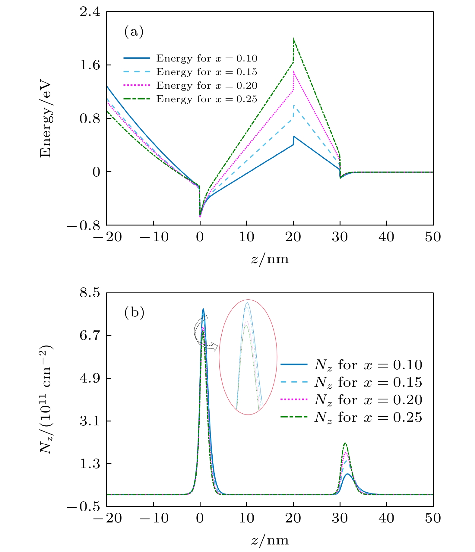
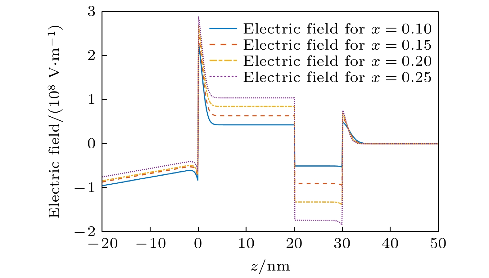
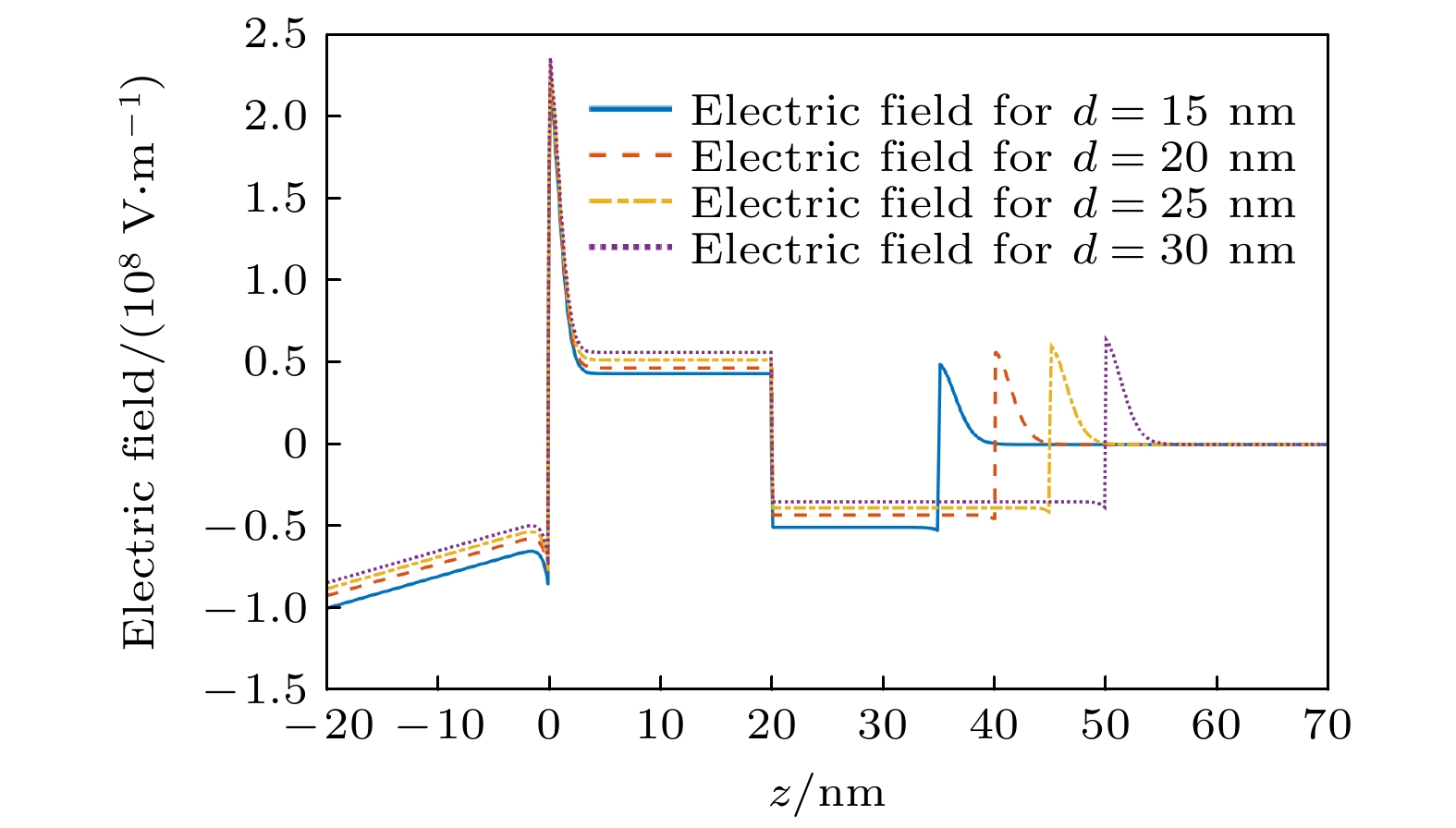
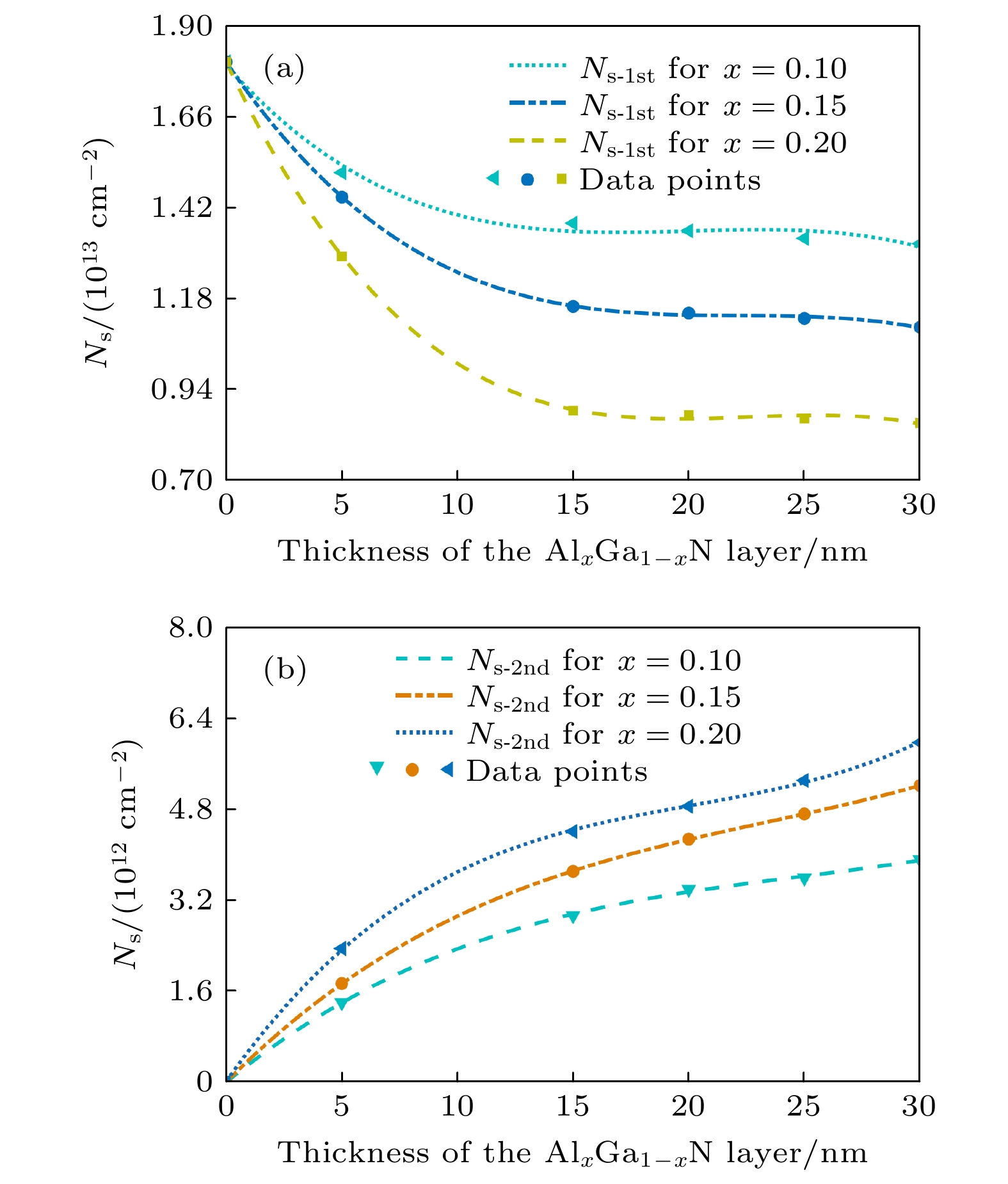
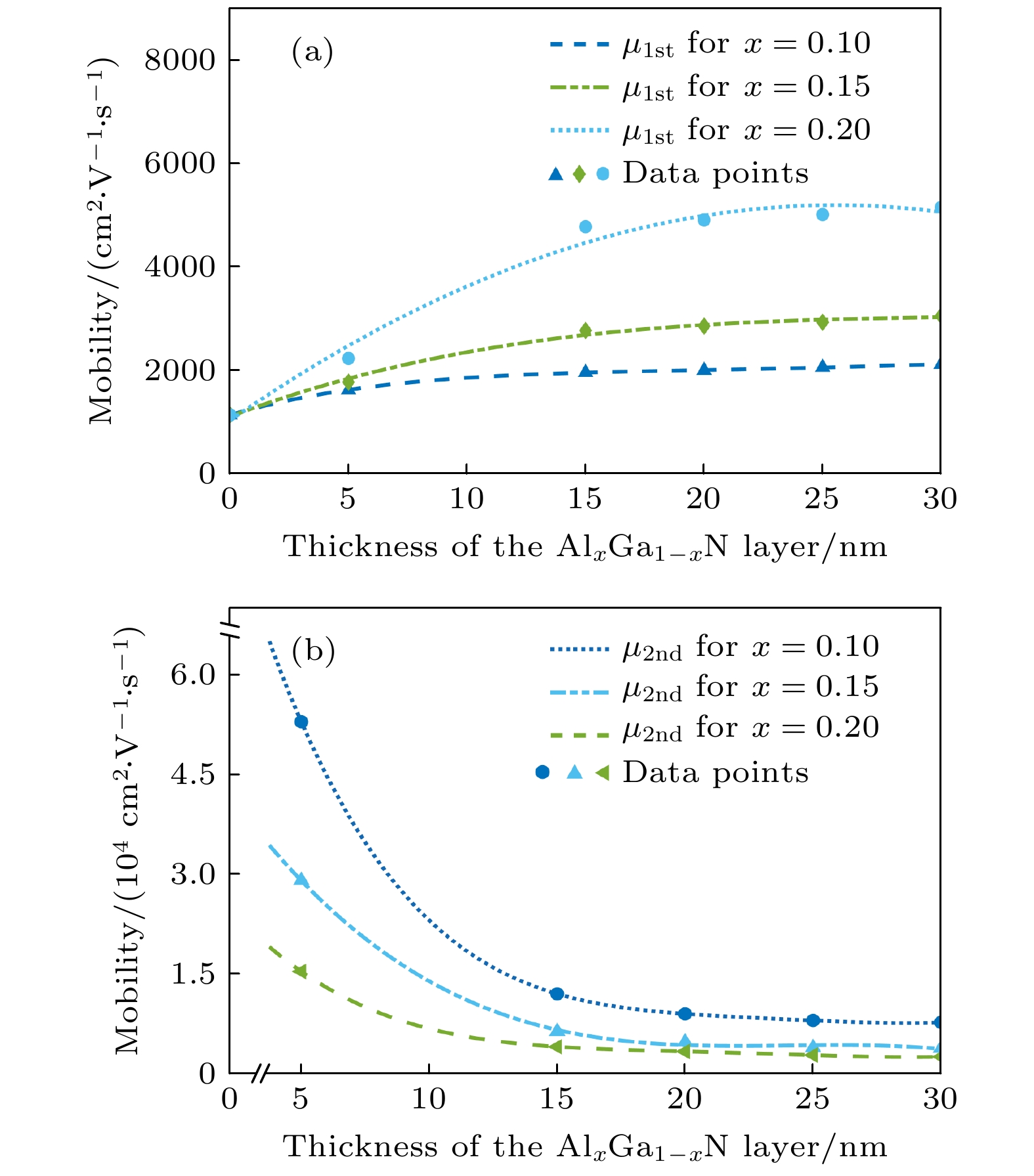
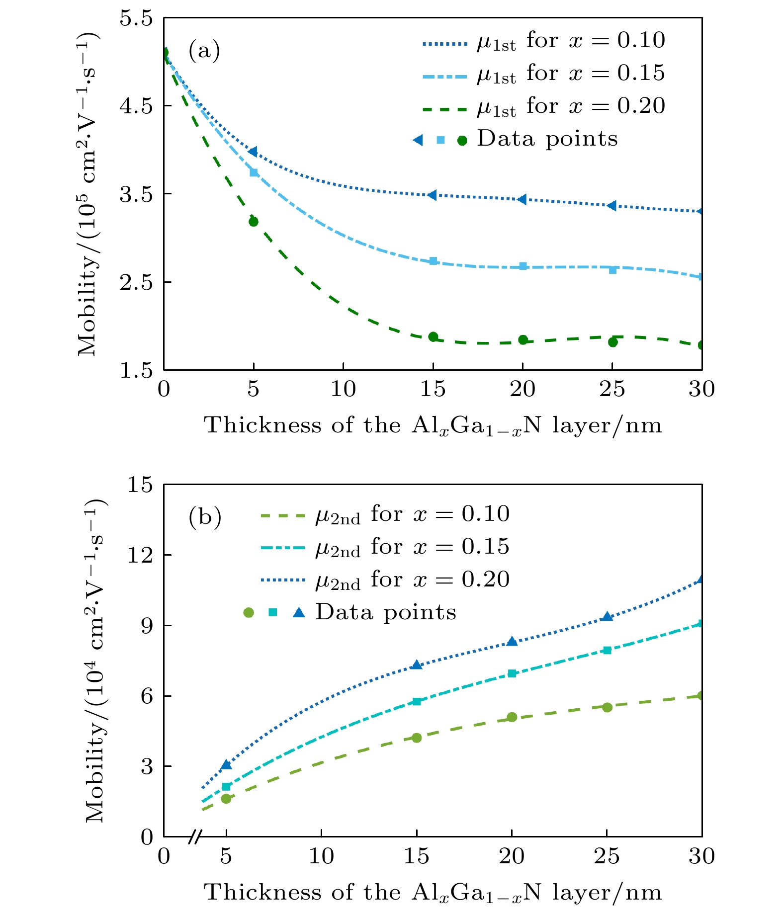
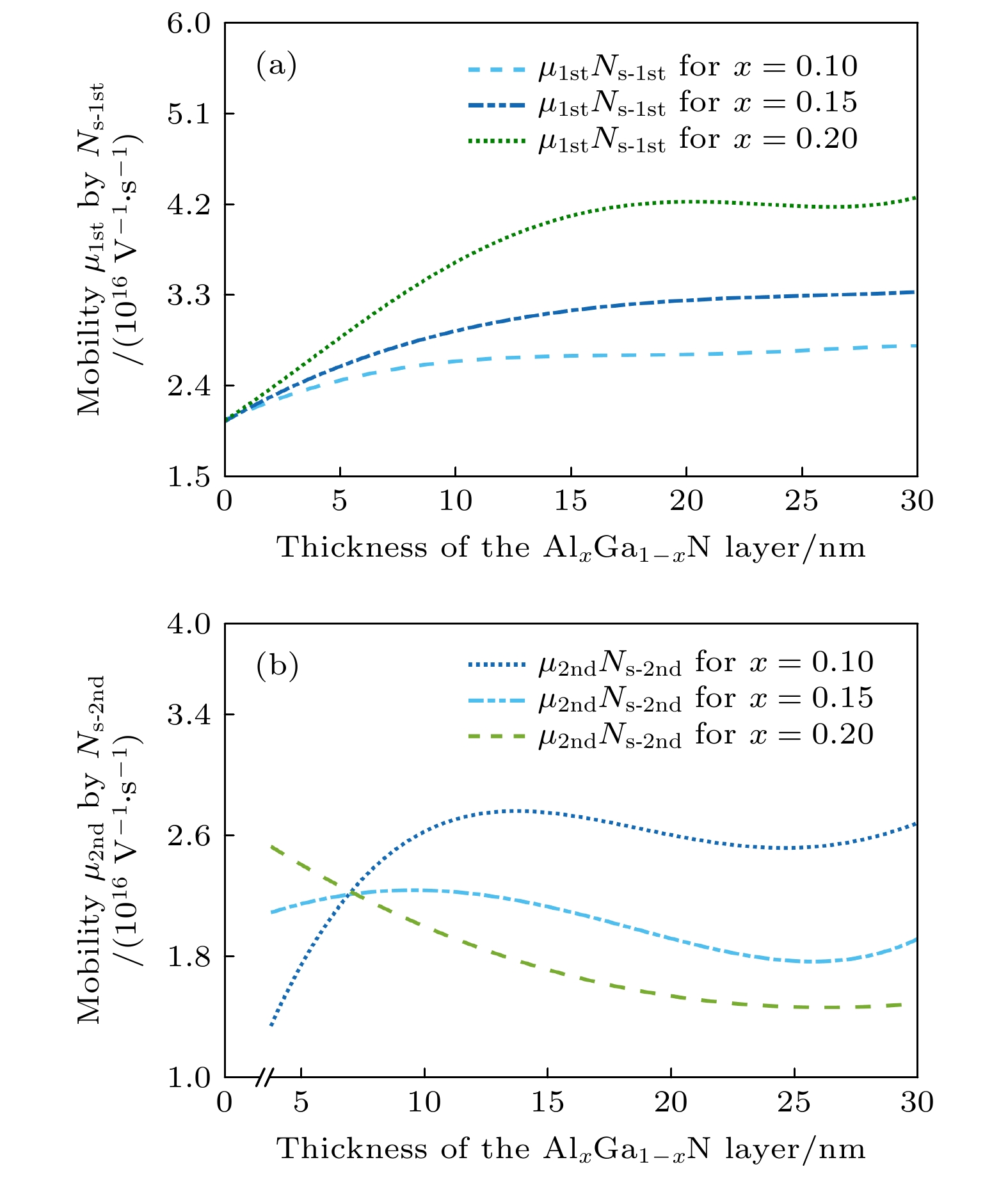
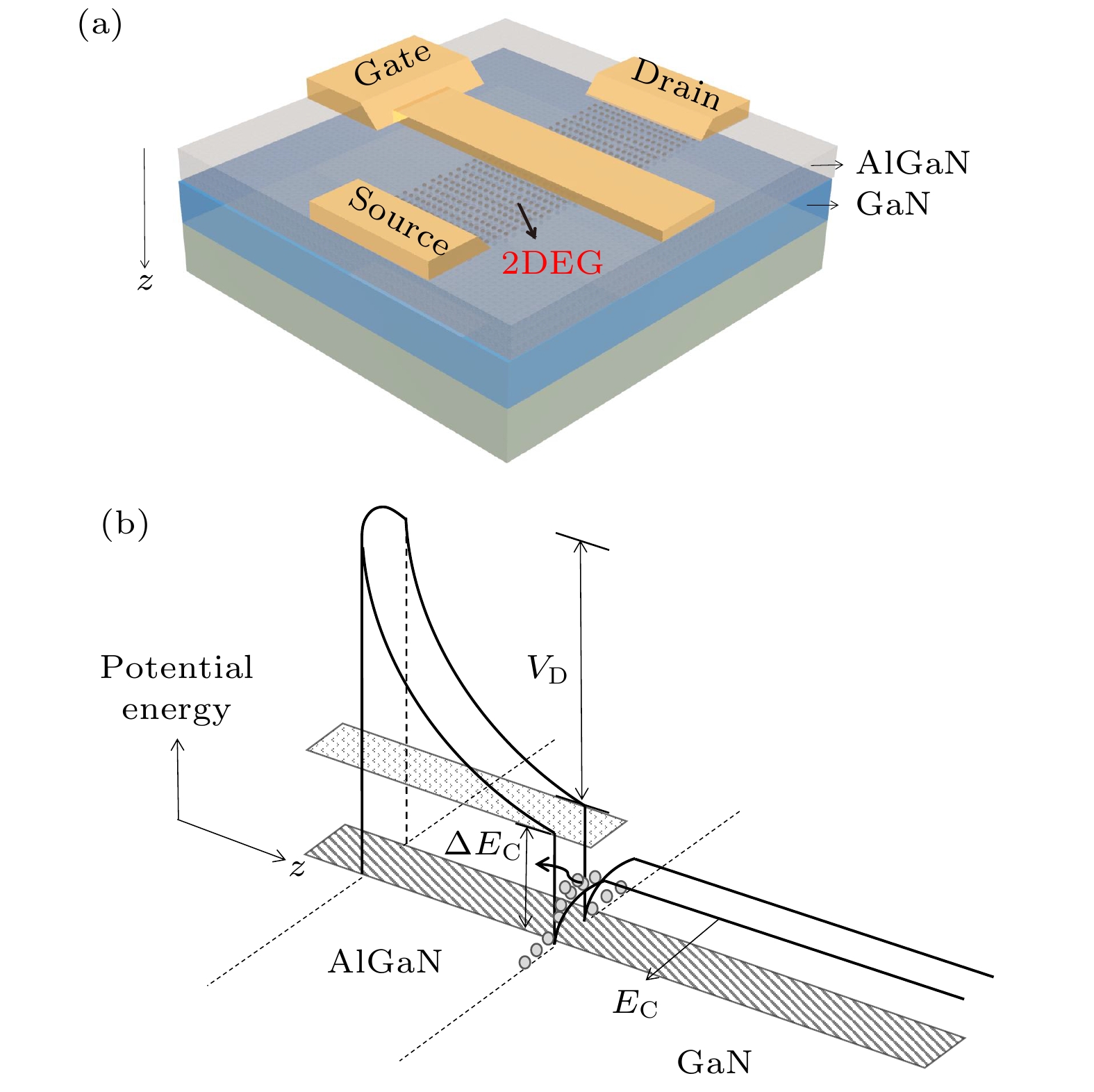
With the demand for high-temperature, high-frequency, and high-power microwave applications increasing, AlGaN/GaN high electron mobility transistors (HEMT) have attracted much attention in recent years. Two-dimensional electron gas (2DEG) induced by spontaneous polarization and piezoelectric polarization caused by the uneven charge distribution on Ga-N bond and the large tensile strain guarantees the high performance of AlGaN/GaN HEMT. Compared with single-channel devices, dual-channel AlGaN/GaN HEMT has great application prospects in enhancing the electronic confinement, current drive and alleviating the current collapse. In order to study the physical characteristics, the carrier state and transportation characterization of n-Al0.3Ga0.7N/GaN/i-AlxGa1–xN/GaN multilayer structure are investigated. By calculating the one-dimensional self-consistent Poisson-Schrödinger, the energy band diagram, electric field and charge distribution in the devices are obtained. The 2DEG, alloy disorder and dislocation scattering mechanism in the device are also analyzed by analytical models in which the wave function in finite barriers and Fermi’s rule are used. With AlxGa1–xN layer thickness increasing from 0 nm to 30 nm and Al content rising from 0.1 to 0.2, the concentration of 2DEG localized in the heterointerface is diminished in the first channel. Simultaneously, mobility limited by alloy disorder scattering increases monotonically with the r composition occupation number and the AlxGa1–xN thickness proportion increasing. Besides, dislocation scattering on carriers is strengthened in the same quantum well, resulting in the lower mobility. In the second channel, 2DEG density gets growing when the variables mentioned above is enlarged. The mobility restricted by alloy disorder scattering shows a reverse trend with the variation of the AlxGa1–xN thickness and Al fraction, which more greatly affect the carriers in the parasitic channel due to the lower barrier height and high permeable carriers. Furthermore, the effect of dislocation scattering on channel electrons is gradually weakened, resulting in an increasing mobility. In general, The dislocation scattering effect in the second channel is intenser than that in the first channel. -
Keywords:
- double-channel /
- two-dimensional electron gas /
- mobility
[1] Mishra U K, Parikh P, Wu Y F 2002 Proc. IEEE 90 1022
 Google Scholar
[2] Mohammad S N, Salvador A A, Morkoc H 1995 Proc. IEEE 83 1306
 Google Scholar
[3] Ibbetson J P, Fini P T, Ness K D, DenBaars S P, Speck J S, Mishrab U K 2000 Appl. Phys. Lett. 77 250
 Google Scholar
[4] 王现彬, 赵正平, 冯志红 2014 物理学报 63 080202
 Google Scholar
Wang X B, Zhao Z P, Feng Z H 2014 Acta Phys. Sin. 63 080202
 Google Scholar
[5] 张雪冰, 刘乃漳, 姚若河 2020 物理学报 69 157303
 Google Scholar
Zhang X B, Liu N Z, Yao R H 2020 Acta Phys. Sin. 69 157303
 Google Scholar
[6] Kranti A, Haldar S, Gupta R S 2002 Solid-State Electron. 46 621
 Google Scholar
[7] Kwon H K, Eiting C J, Lambert D J H, Shelton B S, Wong M M, Zhu T G, Dupuisa R D 1999 Appl. Phys. Lett. 75 2788
 Google Scholar
[8] Chu R M, Zhou Y G, Zheng Y D, Han P, Shen B, Gu S 2001 Appl. Phys. Lett. 79 2270
 Google Scholar
[9] Fan Z F, Lu C Z, Botchkarev A E, Tang H, Salvador A, Aktas O, Kim W, Morkog H 1997 Electron. Lett. 33 814
 Google Scholar
[10] Gaska R, Shur M S, Fjeldly T A 1999 J. Appl. Phys. 85 3009
 Google Scholar
[11] Chu R, Zhou Y, Jie L, Wang D, Chen K J, Lau K M 2005 IEEE Trans. Electron Devices 52 438
 Google Scholar
[12] Quan S, Hao Y, Ma X, Zheng P, Xie Y 2010 J. Semicond. 31 044003
 Google Scholar
[13] Zhang Y., Li Y., Wang J, Shen Y, Hao Y 2020 Nanoscale Res. Lett. 15 1
 Google Scholar
[14] 王冲, 赵梦荻, 裴九清 2016 物理学报 65 038501
 Google Scholar
Wang C, Zhao M D, Pei J Q 2016 Acta Phys. Sin. 65 038501
 Google Scholar
[15] Lee Y J, Yao Y C, Huang C Y, Lin T Y, Cheng L L, Liu C Y, Wang M T Hwang J M 2014 Nanoscale Res. Lett. 9 433
 Google Scholar
[16] Chakraborty A, Ghosh S, Mukhopadhyay P, Jana S K, Dinara S M, Bag A, Mahata M K, Kumar R, Das S, Das P, Biswas D 2016 Electron. Mater. Lett. 12 232
 Google Scholar
[17] Chen C Q, Zhang J P 2003 Appl. Phys. Lett. 82 4593
 Google Scholar
[18] Visalli D, Hove M V, Derluyn J, Cheng K, Degroote S, Leys M, Germain M, Borghs G 2009 Phys. Status Solidi C 6 S988
[19] Yu H B, Lisesivdin S B, Bolukbas B, Kelekci O, Ozturk M K, Ozcelik S, Caliskan D, Ozturk M, Cakmak H, Demirel P, Ozbay E 2010 Phys. Status Solidi A 207 2593
 Google Scholar
[20] Martins J L, Zunger A 1984 Phys. Rev. B 30 6217
 Google Scholar
[21] Fang F F, Howard W E 1966 Phys. Rev. Lett. 16 797
 Google Scholar
[22] Shur M S, Bykhovski A D, Gaska R 2000 Solid-State Electron. 44 205
 Google Scholar
[23] Walukiewicz W, Ruda H E 1984 Phys. Rev. B 30 4571
 Google Scholar
[24] Jena D, Gossard A C, Mishra U K 2000 Appl. Phys. Lett. 76 1707
 Google Scholar
[25] Miyoshi M, Egawa T, Ishikawa H 2015 J. Vac. Sci. Technol. , B 23 1527
[26] Leung K, Wright A F, Stechel E B 1999 Appl. Phys. Lett. 74 2495
 Google Scholar
-
表 1 AlN, GaN和AlxGa1–xN的各项结构参数(300 K)
Table 1. The key parameters of AlN, GaN and AlxGa1 – xN at temperature 300 K.
参数 AlN GaN AlxGa1–xN A/(10–10 nm) 3.112 3.189 C13/GPa 108 103 C33/GPa 373 405 xPAlN + (1 – x) PGaN e31/(C·m–2) –0.6 –0.49 e33/(C·m–2) 1.46 0.73 PSP/(C·m–2) –0.081 –0.029 表 2 沟道中2DEG在基态上的占比
Table 2. The proportion of 2DEG at the ground-state energy in channel 1 & channel 2.
x = 0.1 x = 0.15 x = 0.2 x = 0.25 Nz–1 st在基态E0上的占比 0.9451 0.9669 0.9872 0.9909 Nz–2 nd在基态E0上的占比 0.9651 0.9748 0.9850 0.9908 -
[1] Mishra U K, Parikh P, Wu Y F 2002 Proc. IEEE 90 1022
 Google Scholar
[2] Mohammad S N, Salvador A A, Morkoc H 1995 Proc. IEEE 83 1306
 Google Scholar
[3] Ibbetson J P, Fini P T, Ness K D, DenBaars S P, Speck J S, Mishrab U K 2000 Appl. Phys. Lett. 77 250
 Google Scholar
[4] 王现彬, 赵正平, 冯志红 2014 物理学报 63 080202
 Google Scholar
Wang X B, Zhao Z P, Feng Z H 2014 Acta Phys. Sin. 63 080202
 Google Scholar
[5] 张雪冰, 刘乃漳, 姚若河 2020 物理学报 69 157303
 Google Scholar
Zhang X B, Liu N Z, Yao R H 2020 Acta Phys. Sin. 69 157303
 Google Scholar
[6] Kranti A, Haldar S, Gupta R S 2002 Solid-State Electron. 46 621
 Google Scholar
[7] Kwon H K, Eiting C J, Lambert D J H, Shelton B S, Wong M M, Zhu T G, Dupuisa R D 1999 Appl. Phys. Lett. 75 2788
 Google Scholar
[8] Chu R M, Zhou Y G, Zheng Y D, Han P, Shen B, Gu S 2001 Appl. Phys. Lett. 79 2270
 Google Scholar
[9] Fan Z F, Lu C Z, Botchkarev A E, Tang H, Salvador A, Aktas O, Kim W, Morkog H 1997 Electron. Lett. 33 814
 Google Scholar
[10] Gaska R, Shur M S, Fjeldly T A 1999 J. Appl. Phys. 85 3009
 Google Scholar
[11] Chu R, Zhou Y, Jie L, Wang D, Chen K J, Lau K M 2005 IEEE Trans. Electron Devices 52 438
 Google Scholar
[12] Quan S, Hao Y, Ma X, Zheng P, Xie Y 2010 J. Semicond. 31 044003
 Google Scholar
[13] Zhang Y., Li Y., Wang J, Shen Y, Hao Y 2020 Nanoscale Res. Lett. 15 1
 Google Scholar
[14] 王冲, 赵梦荻, 裴九清 2016 物理学报 65 038501
 Google Scholar
Wang C, Zhao M D, Pei J Q 2016 Acta Phys. Sin. 65 038501
 Google Scholar
[15] Lee Y J, Yao Y C, Huang C Y, Lin T Y, Cheng L L, Liu C Y, Wang M T Hwang J M 2014 Nanoscale Res. Lett. 9 433
 Google Scholar
[16] Chakraborty A, Ghosh S, Mukhopadhyay P, Jana S K, Dinara S M, Bag A, Mahata M K, Kumar R, Das S, Das P, Biswas D 2016 Electron. Mater. Lett. 12 232
 Google Scholar
[17] Chen C Q, Zhang J P 2003 Appl. Phys. Lett. 82 4593
 Google Scholar
[18] Visalli D, Hove M V, Derluyn J, Cheng K, Degroote S, Leys M, Germain M, Borghs G 2009 Phys. Status Solidi C 6 S988
[19] Yu H B, Lisesivdin S B, Bolukbas B, Kelekci O, Ozturk M K, Ozcelik S, Caliskan D, Ozturk M, Cakmak H, Demirel P, Ozbay E 2010 Phys. Status Solidi A 207 2593
 Google Scholar
[20] Martins J L, Zunger A 1984 Phys. Rev. B 30 6217
 Google Scholar
[21] Fang F F, Howard W E 1966 Phys. Rev. Lett. 16 797
 Google Scholar
[22] Shur M S, Bykhovski A D, Gaska R 2000 Solid-State Electron. 44 205
 Google Scholar
[23] Walukiewicz W, Ruda H E 1984 Phys. Rev. B 30 4571
 Google Scholar
[24] Jena D, Gossard A C, Mishra U K 2000 Appl. Phys. Lett. 76 1707
 Google Scholar
[25] Miyoshi M, Egawa T, Ishikawa H 2015 J. Vac. Sci. Technol. , B 23 1527
[26] Leung K, Wright A F, Stechel E B 1999 Appl. Phys. Lett. 74 2495
 Google Scholar
Catalog
Metrics
- Abstract views: 6420
- PDF Downloads: 153
- Cited By: 0


 DownLoad:

