


-
Bi2O2Se is a new type of semiconductor material, which has the advantages of high carrier mobility, air stability, strong spin-orbit coupling, etc. It has a variety of synthesis methods and a wide range of applications. In the past few years, many explorations have been made in the synthesis, large-size growth, and applications of Bi2O2Se. It has been applied to field effect transistors, infrared photodetectors, semiconductor devices, heterojunctions, spin electronics, etc. Since nanowire has a larger surface area-to-volume ratio than nano-film, nanowire may have greater advantages in gate regulation and strong spin-orbit coupling, and these properties can play a crucial role in certain fields. However, most of the studies focused on its two-dimensional films, and there are less researches of its one-dimensional counterpart. In this work, a method of growing Bi2O2Se one-dimensional nanowires by chemical vapor deposition in a three-temperature-zone tubular furnace is introduced. High-quality suspended Bi2O2Se nanowires are obtained. In addition, the effects on the Bi2O2Se nanowire growth of the position of the mica substrates, i.e, different horizontal positions and vertical heights in the quartz boat, are studied, and the optimal conditions for the growth are summarized. The nanowires are characterized by atomic force microscope and energy dispersive spectrometer to show the information about the size and component. Then, superconducting quantum interference device based on the Bi2O2Se nanowires is constructed, and the superconducting quantum interference in a magnetic field is observed, which provides a way to broaden the application of Bi2O2Se nanowires.
-
Keywords:
- Bi2O2Se nanowires /
- chemical vapor deposition /
- superconducting quantum interference devices
[1] Wu J X, Yuan H T, Meng M M, Chen C, Sun Y, Chen Z Y, Dang W H, Tan C W, Liu Y J, Yin J B, Zhou Y B, Huang S Y, Xu H Q, Cui Y, Hwang H Y, Liu Z F, Chen Y L, Yan B H, Peng H L 2017 Nat. Nanotechnol. 12 530
 Google Scholar
[2] Wu J, Tan C, Tan Z, Liu Y, Yin J, Dang W, Wang M, Peng H 2017 Nano Lett. 17 3021
Google Scholar
[3] Zhao K, Liu H, Tan C, Xiao J, Shen J, Liu G, Peng H, Lu L, Qu F 2022 Appl. Phys. Lett. 121 212104
Google Scholar
[4] Wu J X, Liu Y J, Tan Z, Tan C, Yin J B, Li T, Tu T, Peng H 2017 Adv. Mater. 29 1704060
Google Scholar
[5] Meng M M, Huang S Y, Tan C, Wu J X, Jing Y, Peng H, Xu H Q 2018 Nanoscale 10 2704
Google Scholar
[6] Meng M M, Huang S Y, Tan C, Wu J X, Li X, Peng H, Xu H Q 2019 Nanoscale 11 10622
Google Scholar
[7] Li J, Wang Z, Wen Y, Chu J, Yin L, Cheng R, Lei L, He P, Jiang C, Feng L, He J 2018 Adv. Funct. Mater. 28 1706437
Google Scholar
[8] Xu S, Fu H, Tian Y, Deng T, Cai J, Wu J, Tu T, Li T, Tan C, Liang Y, Zhang C, Liu Z, Liu Z, Chen Y, Jiang Y, Yan B, Peng H 2020 Angew. Chem. Int. Ed. 59 17938
Google Scholar
[9] Hong C Y, Tao Y, Nie A M, Zhang M H, Wang N, Li R P, Huang J Q, Huang Y Q, Ren X M, Cheng Y C, Liu X L 2020 ACS Nano 14 16803
Google Scholar
[10] Song Y, Li Z, Li H, Tang S, Mu G, Xu L, Peng W, Shen D, Chen Y, Xie X, Jiang M 2020 Nanotechnology 31 165704
Google Scholar
[11] Ghosh T, Samanta M, Vasdev A, Dolui K, Ghatak J, Das T, Sheet G, Biswas K 2019 Nano Lett. 19 5703
Google Scholar
[12] Khan U, Luo Y, Tang L, Teng C, Liu J, Liu B, Cheng H M 2019 Adv. Funct. Mater. 29 1807979
Google Scholar
[13] Wu Z, Liu G L, Wang Y X, Yang X, Wei T Q, Wang Q J, Liang J, Xu N, Li Z Z, Zhu B, Qi H S, Deng Y, Zhu J 2019 Adv. Funct. Mater. 29 1906639
Google Scholar
[14] Liu S, Tan C, He D, Wang Y, Peng H, Zhao H 2020 Adv. Optical Mater. 8 1901567
Google Scholar
[15] Zou X, Sun Y, Wang C 2022 Small Methods 6 2200347
Google Scholar
[16] Khan U, Nairan A, Khan K, Li S, Liu B, Gao J 2022 Small 19 2206648
Google Scholar
[17] Khan U, Tang L, Ding B, Yuting L, Feng S, Chen W, Khan M J, Liu B, Cheng H M 2021 Adv. Funct. Mater. 31 2101170
Google Scholar
[18] Yu J, Sun Q 2018 Appl. Phys. Lett. 112 053901
Google Scholar
[19] Mao Q, Geng X, Yang J, Zhang J, Zhu S, Yu Q, Wang Y, Li H, Li R, Hao H 2018 J. Cryst. Growth. 498 244
Google Scholar
[20] Kim M, Park D, Kim J 2021 J. Alloy. Compd. 851 156905
Google Scholar
[21] Li J, Wang Z, Chu J, Cheng Z, He P, Wang J, Yin L, Cheng R, Li N, Wen Y, He J 2019 Appl. Phys. Lett. 114 151104
Google Scholar
[22] Bluhm H, Foletti S, Neder I, Rudner M, Mahalu D, Umansky V, Yacoby A 2010 Nat. Phys. 7 109
Google Scholar
[23] Quhe R, Liu J, Wu J, Yang J, Wang Y, Li Q, Li T, Guo Y, Yang J, Peng H, Lei M, Lu J 2019 Nanoscale 11 532
Google Scholar
[24] Yin J, Tan Z, Hong H, Wu J, Yuan H, Liu Y, Chen C, Tan C, Yao F, Li T, Chen Y, Liu Z, Liu K, Peng H 2018 Nat. Commun. 9 3311
Google Scholar
[25] Fan C, Dai B, Liang H, Xu X, Qi Z, Jiang H, Duan H, Zhang Q 2021 Adv. Funct. Mater. 31 2010263
Google Scholar
[26] Jiang K, Hu J 2022 Nat. Phys. 18 1145
Google Scholar
[27] Mayer W, Dartiailh M C, Yuan J, Wickramasinghe K S, Rossi E, Shabani J 2020 Nat. Commun. 11 212
Google Scholar
[28] Fukaya Y, Tanaka Y, Gentile P, Yada K, Cuoco M 2022 npj Quantum Mater. 7 99
Google Scholar
[29] Jiang D, Yu D Y, Zheng Z, Cao X C, Lin Q, Liu W M 2022 Acta Phys. Sin. 71 160302
Google Scholar
[30] Frolov S M, Manfra M J, Sau J D 2020 Nat. Phys. 16 718
Google Scholar
[31] Breunig O, Ando Y 2021 Nat. Rev. Phys. 4 184
Google Scholar
[32] Matsuo S, Imoto T, Yokoyama T, Sato Y, Lindemann T, Gronin S, Gardner G C, Manfra M J, Tarucha S 2023 Nat. Phys. 19 1636
Google Scholar
[33] Mourik V, Zuo K, Frolov S M, Plissard S R, Bakkers E P A M, Kouwenhoven L P 2012 Science 336 1003
Google Scholar
[34] Dvir T, Wang G, van Loo N, Liu C X, Mazur G P, Bordin A, ten Haaf S L D, Wang J Y, van Driel D, Zatelli F, Li X, Malinowski F K, Gazibegovic S, Badawy G, Bakkers E P A M, Wimmer M, Kouwenhoven L P 2023 Nature 614 445
Google Scholar
[35] Deng M T, Vaitiekėnas S, Hansen E B, Danon J, Leijnse M, Flensberg K, Nygård J, Krogstrup P, Marcus C M 2016 Science 354 1557
Google Scholar
[36] Pal B, Chakraborty A, Sivakumar P K, Davydova M, Gopi A K, Pandeya A K, Krieger J A, Zhang Y, Date M, Ju S, Yuan N, Schröter N B M, Fu L, Parkin S S P 2022 Nat. Phys. 18 1228
Google Scholar
[37] Chen A Q, Park M J, Gill S T, Xiao Y R, Reigi-Plessis D, MacDougall G J, Gilbert M J, Mason N 2018 Nat. Commun. 9 3478
Google Scholar
-
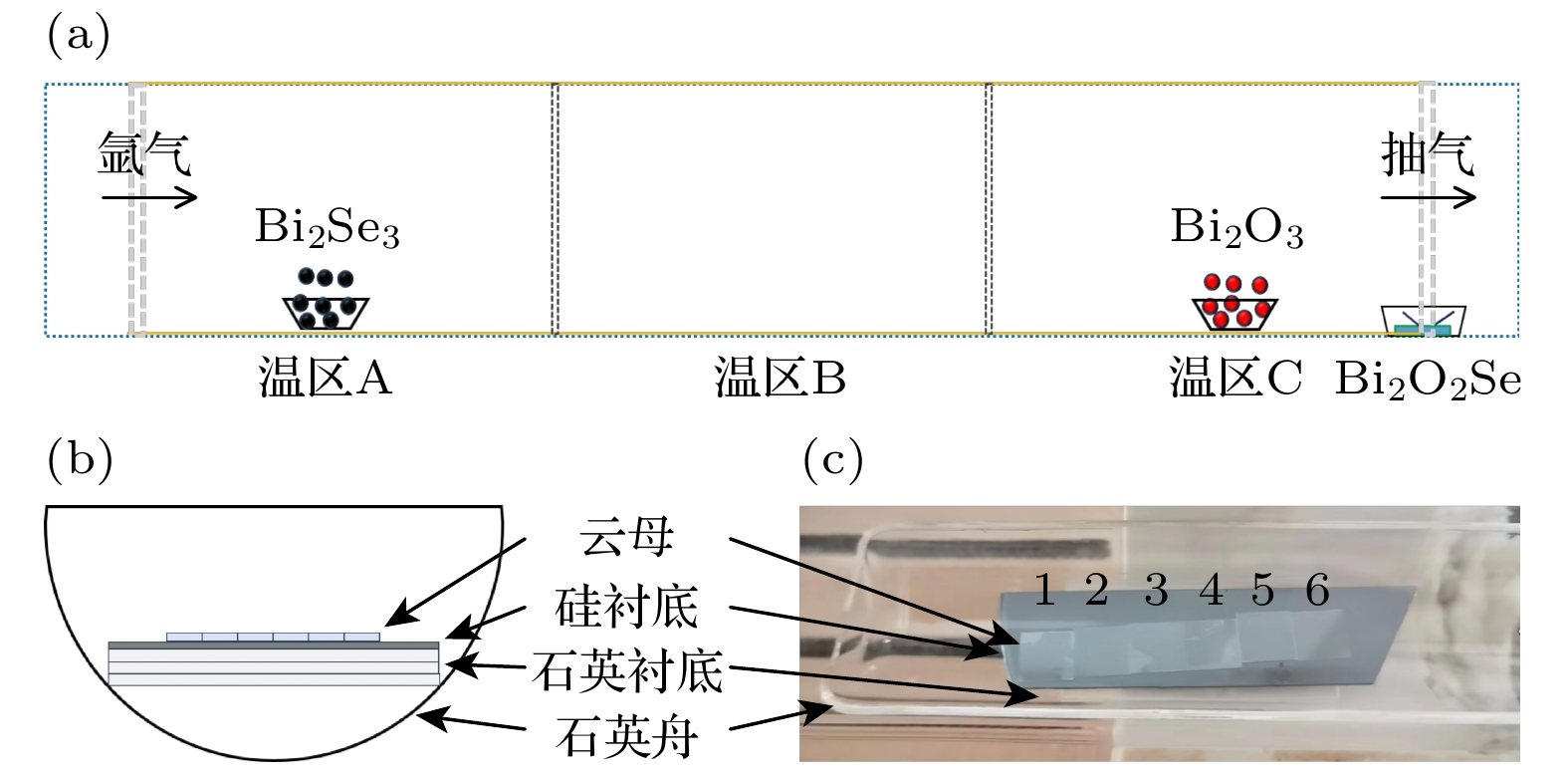
图 1 (a)三温区管式炉的示意图, Bi2Se3粉末放置在温区A的中央, Bi2O3粉末放置在温区C的中央, 带有云母衬底的石英舟放置在管式炉的右边缘. (b), (c)带有云母衬底的石英舟的示意图和光学照片
Figure 1. (a) Schematic diagram of the three-temperature-zone tubular furnace, with Bi2Se3 powder placed at the center of zone A and Bi2O3 powder at the center of zone C, a quartz boat with mica substrates is placed at the right edge of the quartz tube. (b), (c) Schematic diagram and optical photograph of a quartz boat with mica substrates, respectively.
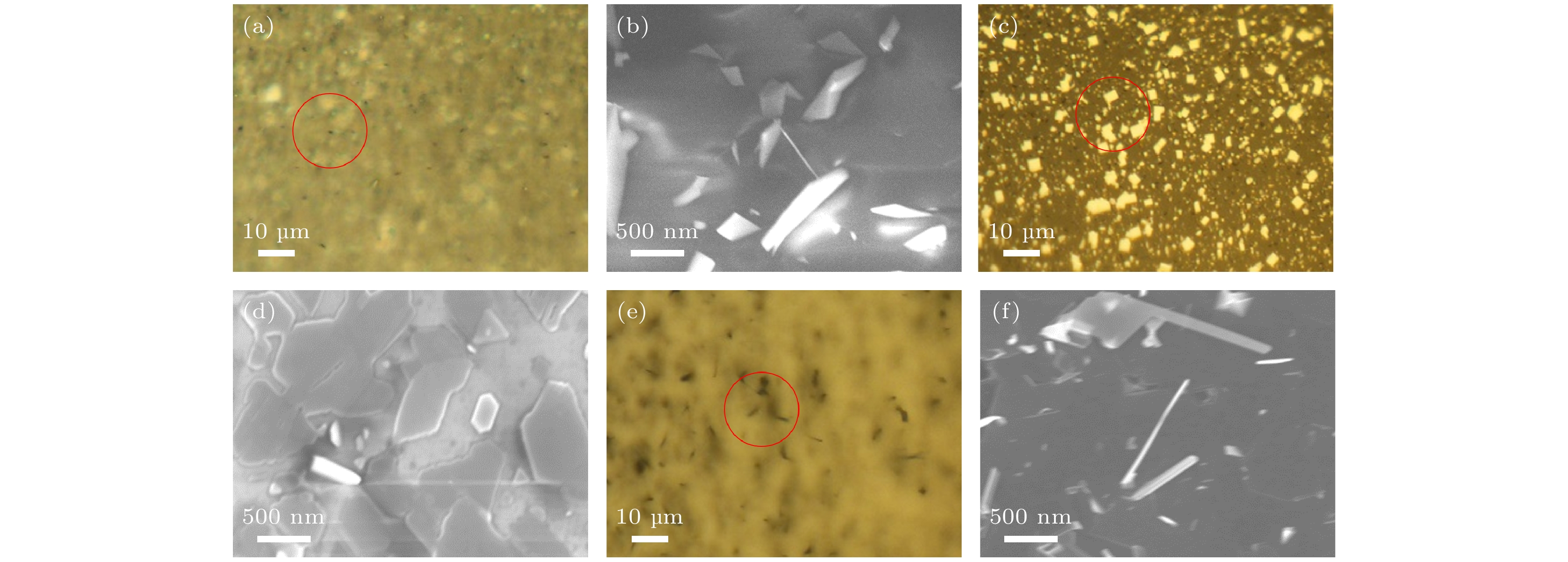
图 2 不同水平位置的云母衬底生长的Bi2O2Se光学显微镜照片和SEM照片 (a), (c), (e)对应2号、4号和5号云母衬底生长Bi2O2Se后的光学显微镜照片; (b), (d), (f)对应2号、4号和5号云母衬底生长Bi2O2Se后的SEM照片
Figure 2. Optical microscope photos and SEM photos of Bi2O2Se grown on mica substrates at different horizontal positions: (a), (c), (e) Optical microscope photos of Bi2O2Se grown on mica substrates at positions No.2, No.4 and No.5, respectively; (b), (d), (f) SEM photos of Bi2O2Se grown on mica substrates at positions No.2, No.4 and No.5, respectively.
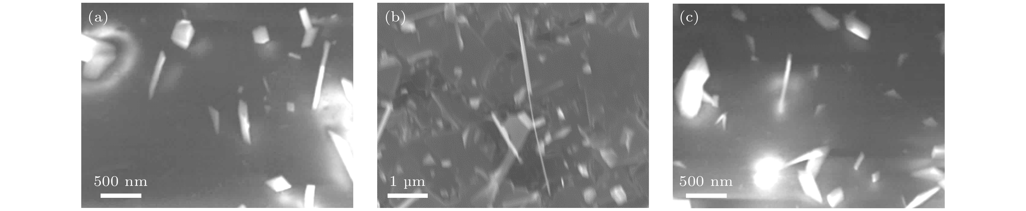
图 3 不同竖直高度的云母衬底生长的Bi2O2Se纳米线的SEM照片 (a)—(c)石英衬底数量为1个、8个和13个
Figure 3. SEM photos of Bi2O2Se nanowires grown on mica substrates of different vertical heights: (a)–(c) There are 1, 8 and 13 quartz substrates, respectively.
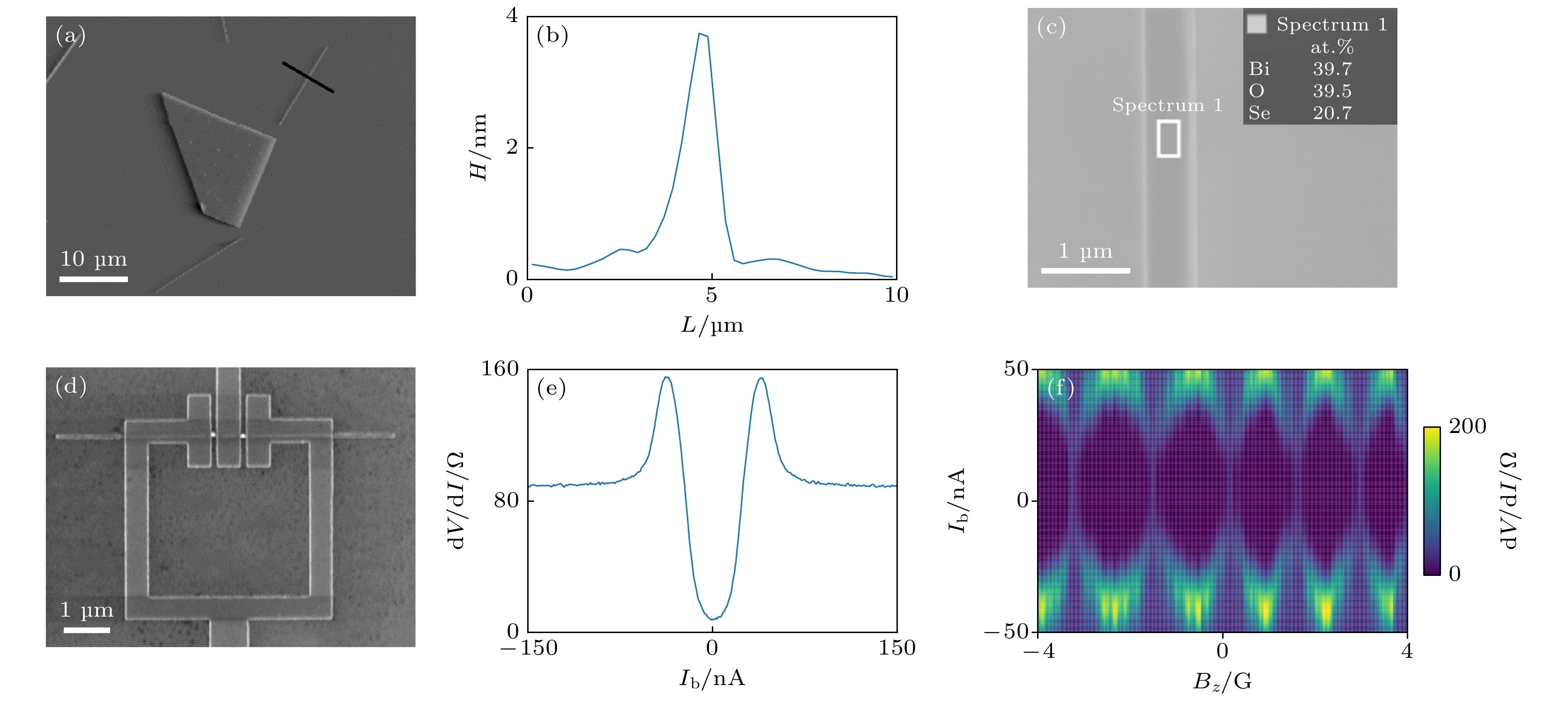
图 4 (a), (b) Bi2O2Se纳米线的AFM表征; (c) Bi2O2Se纳米线的EDS能谱; (d)使用Bi2O2Se纳米线制备的SQUID的SEM照片; (e) SQUID的dV/dI-Ib曲线; (d) SQUID干涉图案
Figure 4. (a), (b) AFM characterization of Bi2O2Se nanowire; (c) EDS spectra of Bi2O2Se nanowire; (d) SEM images of SQUID device; (e) dV/dI-Ib curve of SQUID; (f) SQUID interference pattern.
表 1 Bi2O2Se纳米线的生长步骤
Table 1. Growth steps of Bi2O2Se nanowires.
步骤 第1步 第2步 第3步 第4步 温区A
(Bi2Se3)温度/℃ 室温—100 100—580 580 580—室温 时间/min 5 25 30 — 温区B 温度/℃ 室温—100 100—610 610 610—室温 时间/min 5 30 25 — 温区C
(Bi2O3)温度/℃ 室温—100 100—630 630 630—室温 时间/min 5 30 25 —  DownLoad: CSV
-
[1] Wu J X, Yuan H T, Meng M M, Chen C, Sun Y, Chen Z Y, Dang W H, Tan C W, Liu Y J, Yin J B, Zhou Y B, Huang S Y, Xu H Q, Cui Y, Hwang H Y, Liu Z F, Chen Y L, Yan B H, Peng H L 2017 Nat. Nanotechnol. 12 530
Google Scholar
[2] Wu J, Tan C, Tan Z, Liu Y, Yin J, Dang W, Wang M, Peng H 2017 Nano Lett. 17 3021
Google Scholar
[3] Zhao K, Liu H, Tan C, Xiao J, Shen J, Liu G, Peng H, Lu L, Qu F 2022 Appl. Phys. Lett. 121 212104
Google Scholar
[4] Wu J X, Liu Y J, Tan Z, Tan C, Yin J B, Li T, Tu T, Peng H 2017 Adv. Mater. 29 1704060
Google Scholar
[5] Meng M M, Huang S Y, Tan C, Wu J X, Jing Y, Peng H, Xu H Q 2018 Nanoscale 10 2704
Google Scholar
[6] Meng M M, Huang S Y, Tan C, Wu J X, Li X, Peng H, Xu H Q 2019 Nanoscale 11 10622
Google Scholar
[7] Li J, Wang Z, Wen Y, Chu J, Yin L, Cheng R, Lei L, He P, Jiang C, Feng L, He J 2018 Adv. Funct. Mater. 28 1706437
Google Scholar
[8] Xu S, Fu H, Tian Y, Deng T, Cai J, Wu J, Tu T, Li T, Tan C, Liang Y, Zhang C, Liu Z, Liu Z, Chen Y, Jiang Y, Yan B, Peng H 2020 Angew. Chem. Int. Ed. 59 17938
Google Scholar
[9] Hong C Y, Tao Y, Nie A M, Zhang M H, Wang N, Li R P, Huang J Q, Huang Y Q, Ren X M, Cheng Y C, Liu X L 2020 ACS Nano 14 16803
Google Scholar
[10] Song Y, Li Z, Li H, Tang S, Mu G, Xu L, Peng W, Shen D, Chen Y, Xie X, Jiang M 2020 Nanotechnology 31 165704
Google Scholar
[11] Ghosh T, Samanta M, Vasdev A, Dolui K, Ghatak J, Das T, Sheet G, Biswas K 2019 Nano Lett. 19 5703
Google Scholar
[12] Khan U, Luo Y, Tang L, Teng C, Liu J, Liu B, Cheng H M 2019 Adv. Funct. Mater. 29 1807979
Google Scholar
[13] Wu Z, Liu G L, Wang Y X, Yang X, Wei T Q, Wang Q J, Liang J, Xu N, Li Z Z, Zhu B, Qi H S, Deng Y, Zhu J 2019 Adv. Funct. Mater. 29 1906639
Google Scholar
[14] Liu S, Tan C, He D, Wang Y, Peng H, Zhao H 2020 Adv. Optical Mater. 8 1901567
Google Scholar
[15] Zou X, Sun Y, Wang C 2022 Small Methods 6 2200347
Google Scholar
[16] Khan U, Nairan A, Khan K, Li S, Liu B, Gao J 2022 Small 19 2206648
Google Scholar
[17] Khan U, Tang L, Ding B, Yuting L, Feng S, Chen W, Khan M J, Liu B, Cheng H M 2021 Adv. Funct. Mater. 31 2101170
Google Scholar
[18] Yu J, Sun Q 2018 Appl. Phys. Lett. 112 053901
Google Scholar
[19] Mao Q, Geng X, Yang J, Zhang J, Zhu S, Yu Q, Wang Y, Li H, Li R, Hao H 2018 J. Cryst. Growth. 498 244
Google Scholar
[20] Kim M, Park D, Kim J 2021 J. Alloy. Compd. 851 156905
Google Scholar
[21] Li J, Wang Z, Chu J, Cheng Z, He P, Wang J, Yin L, Cheng R, Li N, Wen Y, He J 2019 Appl. Phys. Lett. 114 151104
Google Scholar
[22] Bluhm H, Foletti S, Neder I, Rudner M, Mahalu D, Umansky V, Yacoby A 2010 Nat. Phys. 7 109
Google Scholar
[23] Quhe R, Liu J, Wu J, Yang J, Wang Y, Li Q, Li T, Guo Y, Yang J, Peng H, Lei M, Lu J 2019 Nanoscale 11 532
Google Scholar
[24] Yin J, Tan Z, Hong H, Wu J, Yuan H, Liu Y, Chen C, Tan C, Yao F, Li T, Chen Y, Liu Z, Liu K, Peng H 2018 Nat. Commun. 9 3311
Google Scholar
[25] Fan C, Dai B, Liang H, Xu X, Qi Z, Jiang H, Duan H, Zhang Q 2021 Adv. Funct. Mater. 31 2010263
Google Scholar
[26] Jiang K, Hu J 2022 Nat. Phys. 18 1145
Google Scholar
[27] Mayer W, Dartiailh M C, Yuan J, Wickramasinghe K S, Rossi E, Shabani J 2020 Nat. Commun. 11 212
Google Scholar
[28] Fukaya Y, Tanaka Y, Gentile P, Yada K, Cuoco M 2022 npj Quantum Mater. 7 99
Google Scholar
[29] Jiang D, Yu D Y, Zheng Z, Cao X C, Lin Q, Liu W M 2022 Acta Phys. Sin. 71 160302
Google Scholar
[30] Frolov S M, Manfra M J, Sau J D 2020 Nat. Phys. 16 718
Google Scholar
[31] Breunig O, Ando Y 2021 Nat. Rev. Phys. 4 184
Google Scholar
[32] Matsuo S, Imoto T, Yokoyama T, Sato Y, Lindemann T, Gronin S, Gardner G C, Manfra M J, Tarucha S 2023 Nat. Phys. 19 1636
Google Scholar
[33] Mourik V, Zuo K, Frolov S M, Plissard S R, Bakkers E P A M, Kouwenhoven L P 2012 Science 336 1003
Google Scholar
[34] Dvir T, Wang G, van Loo N, Liu C X, Mazur G P, Bordin A, ten Haaf S L D, Wang J Y, van Driel D, Zatelli F, Li X, Malinowski F K, Gazibegovic S, Badawy G, Bakkers E P A M, Wimmer M, Kouwenhoven L P 2023 Nature 614 445
Google Scholar
[35] Deng M T, Vaitiekėnas S, Hansen E B, Danon J, Leijnse M, Flensberg K, Nygård J, Krogstrup P, Marcus C M 2016 Science 354 1557
Google Scholar
[36] Pal B, Chakraborty A, Sivakumar P K, Davydova M, Gopi A K, Pandeya A K, Krieger J A, Zhang Y, Date M, Ju S, Yuan N, Schröter N B M, Fu L, Parkin S S P 2022 Nat. Phys. 18 1228
Google Scholar
[37] Chen A Q, Park M J, Gill S T, Xiao Y R, Reigi-Plessis D, MacDougall G J, Gilbert M J, Mason N 2018 Nat. Commun. 9 3478
Google Scholar
-
[1] HAO Yulong, PENG Aolin, ZHANG Shiwei, LU Xuemei, ZHOU Jie, HAO Guolin. Precise preparation of two-dimensional heterostructures via chemical vapor deposition: Current status and future prospects. Acta Physica Sinica, 2025, 74(22): 228101. doi: 10.7498/aps.74.20251305 [2] WANG Chengyang, LI Yuexin, HE Yanyan, LI Mei, ZHONG Lun, JIE Wenjing. Controllable synthesis of two-dimensional ferroelectric α-In2Se3 by low-temperature chemical vapor deposition. Acta Physica Sinica, 2025, 74(22): 228102. doi: 10.7498/aps.74.20251070 [3] Fei Xiang, Zhang Xiu-Mei, Fu Quan-Gui, Cai Zheng-Yang, Nan Hai-Yan, Gu Xiao-Feng, Xiao Shao-Qing. Milimeter-level MoS2 monolayers and WS2-MoS2 heterojunctions grown on molten glass by pre-chemical vapor deposition. Acta Physica Sinica, 2022, 71(4): 048101. doi: 10.7498/aps.71.20211735 [4] Wang Hong-Zhang, Li Yu-Long, Xu Tie-Quan, Zhu Zi-Qing, Ma Ping, Wang Yue, Gan Zi-Zhao. Fabrication and characterization of YBa2Cu3O7– $_{ \delta}$ step-edge Josephson junctions on MgO substrate for high-temperature superconducting quantum interference devices. Acta Physica Sinica, 2021, 70(3): 037401. doi: 10.7498/aps.70.20201291[5] Wang Xiao-Yu, Bi Wei-Hong, Cui Yong-Zhao, Fu Guang-Wei, Fu Xing-Hu, Jin Wa, Wang Ying. Synthesis of photonic crystal fiber based on graphene directly grown on air-hole by chemical vapor deposition. Acta Physica Sinica, 2020, 69(19): 194202. doi: 10.7498/aps.69.20200750 [6] Li Dan-Yang, Han Xu, Xu Guang-Yuan, Liu Xiao, Zhao Xiao-Jun, Li Geng-Wei, Hao Hui-Ying, Dong Jing-Jing, Liu Hao, Xing Jie. Bi2O2Se photoconductive detector with low power consumption and high sensitivity. Acta Physica Sinica, 2020, 69(24): 248502. doi: 10.7498/aps.69.20201044 [7] Feng Qiu-Ju, Shi Bo, Li Yun-Zheng, Wang De-Yu, Gao Chong, Dong Zeng-Jie, Xie Jin-Zhu, Liang Hong-Wei. Fabrication and properties of non-balance electric bridge gas sensor based on a single Sb doped ZnO microwire. Acta Physica Sinica, 2020, 69(3): 038102. doi: 10.7498/aps.69.20191530 [8] Zhang Xiao-Bo, Qing Fang-Zhu, Li Xue-Song. Clean transfer of chemical vapor deposition graphene film. Acta Physica Sinica, 2019, 68(9): 096801. doi: 10.7498/aps.68.20190279 [9] Feng Qiu-Ju, Li Fang, Li Tong-Tong, Li Yun-Zheng, Shi Bo, Li Meng-Ke, Liang Hong-Wei. Growth and characterization of grid-like β-Ga2O3 nanowires by electric field assisted chemical vapor deposition method. Acta Physica Sinica, 2018, 67(21): 218101. doi: 10.7498/aps.67.20180805 [10] Wang Bin, Feng Ya-Hui, Wang Qiu-Shi, Zhang Wei, Zhang Li-Na, Ma Jin-Wen, Zhang Hao-Ran, Yu Guang-Hui, Wang Gui-Qiang. Hydrogen etching of chemical vapor deposition-grown graphene domains. Acta Physica Sinica, 2016, 65(9): 098101. doi: 10.7498/aps.65.098101 [11] Ma Li-An, Zheng Yong-An, Wei Zhao-Hui, Hu Li-Qin, Guo Tai-Liang. Effect of synthesis temperature and N2/O2 flow on morphology and field emission property of SnO2 nanowires. Acta Physica Sinica, 2015, 64(23): 237901. doi: 10.7498/aps.64.237901 [12] Wang Lang, Feng Wei, Yang Lian-Qiao, Zhang Jian-Hua. The pre-treatment of copper for graphene synthesis. Acta Physica Sinica, 2014, 63(17): 176801. doi: 10.7498/aps.63.176801 [13] Feng Qiu-Ju, Xu Rui-Zhuo, Guo Hui-Ying, Xu Kun, Li Rong, Tao Peng-Cheng, Liang Hong-Wei, Liu Jia-Yuan, Mei Yi-Ying. Influences of the substrate position on the morphology and characterization of phosphorus doped ZnO nanomaterial. Acta Physica Sinica, 2014, 63(16): 168101. doi: 10.7498/aps.63.168101 [14] Wang Wen-Rong, Zhou Yu-Xiu, Li Tie, Wang Yue-Lin, Xie Xiao-Ming. Research on synthesis of high-quality and large-scale graphene films by chemical vapor deposition. Acta Physica Sinica, 2012, 61(3): 038702. doi: 10.7498/aps.61.038702 [15] Han Dao-Li, Zhao Yuan-Li, Zhao Hai-Bo, Song Tian-Fu, Liang Er-Jun. Growth of well-aligned carbon nanotubes arrays by chemical vapor deposition. Acta Physica Sinica, 2007, 56(10): 5958-5964. doi: 10.7498/aps.56.5958 [16] Guo Ping-Sheng, Chen Ting, Cao Zhang-Yi, Zhang Zhe-Juan, Chen Yi-Wei, Sun Zhuo. Low temperature growth of carbon nanotubes by chemical vapor deposition for field emission cathodes. Acta Physica Sinica, 2007, 56(11): 6705-6711. doi: 10.7498/aps.56.6705 [17] Zeng Xiang-Bo, Liao Xian-Bo, Wang Bo, Diao Hong-Wei, Dai Song-Tao, Xiang Xian-Bi, Chang Xiu-Lan, Xu Yan-Yue, Hu Zhi-Hua, Hao Hui-Ying, Kong Guang-Lin. Boron-doped silicon nanowires grown by plasmaenhanced chemical vapor deposition. Acta Physica Sinica, 2004, 53(12): 4410-4413. doi: 10.7498/aps.53.4410 [18] Yan Xiao-Qin, Liu Zu-Qin, Tang Dong-Sheng, Ci Li-Jie, Liu Dong-Fang, Zhou Zhen-Ping, Liang Ying-Xin, Yuan Hua-Jun, Zhou Wei-Ya, Wang Gang. Effects of substrates on silicon oxide nanowires growth by thermal chemical vapor deposition. Acta Physica Sinica, 2003, 52(2): 454-458. doi: 10.7498/aps.52.454 [19] Yan Gui-Shen, Li He-Jun, Hao Zhi-Biao. . Acta Physica Sinica, 2002, 51(2): 326-331. doi: 10.7498/aps.51.326 [20] CHEN XIAO-HUA, WU GUO-TAO, DENG FU-MING, WANG JIAN-XIONG, YANG HANG-SHENG, WANG MIAO, LU XIAO-NAN, PENG JING-CUI, LI WEN-ZHU. GROWING CARBON BUCKONIONS BY RADIO FREQUENCY PLASMA-ENHANCED CHEMICAL VAPOR DEPOSITION. Acta Physica Sinica, 2001, 50(7): 1264-1267. doi: 10.7498/aps.50.1264 -
 4-20231600Suppl.pdf


 DownLoad:

Catalog
Metrics
- Abstract views: 5135
- PDF Downloads: 180
- Cited By: 0
