-
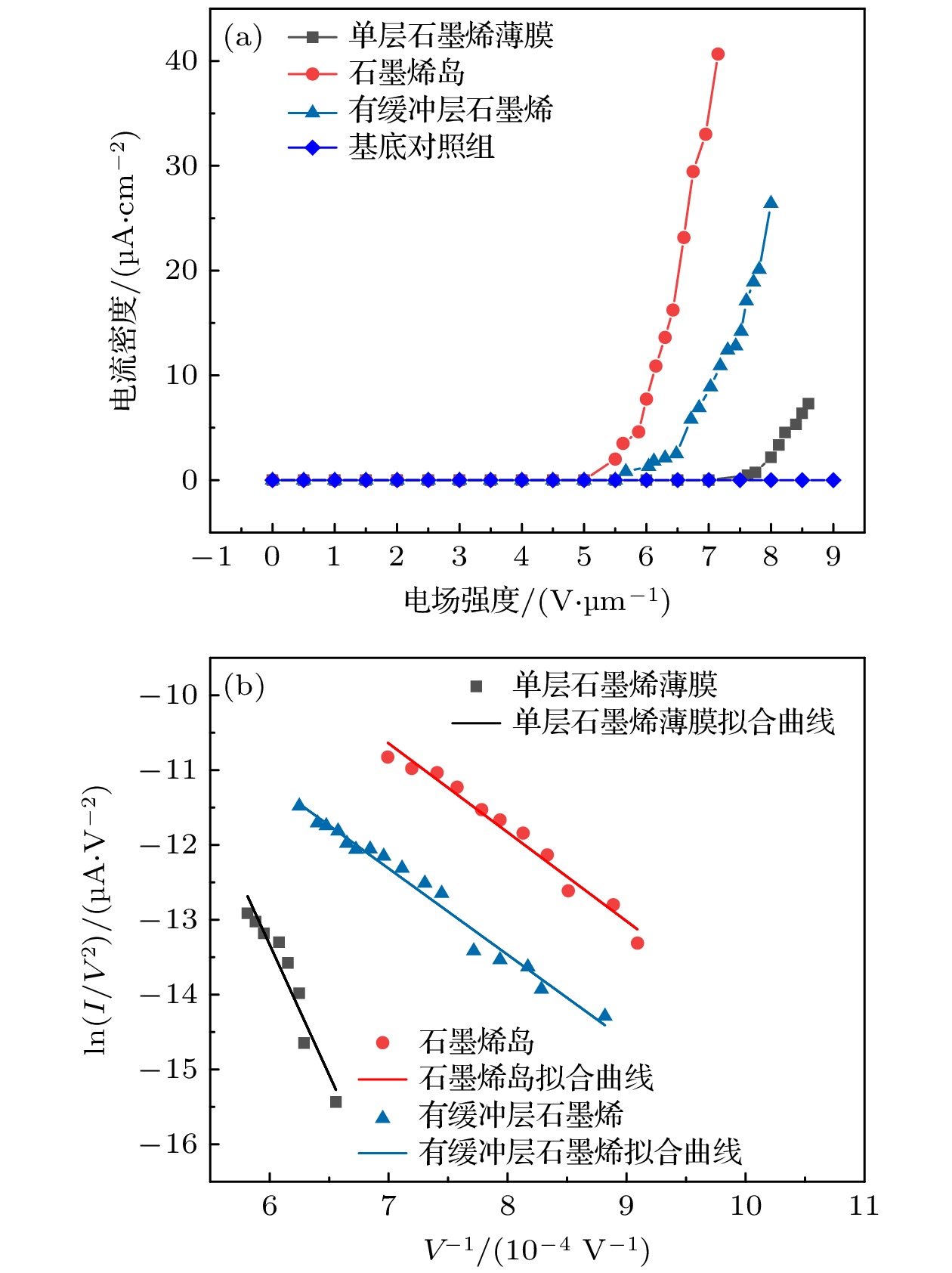
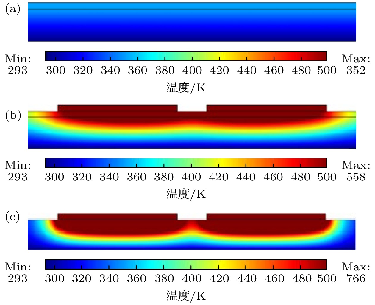
Graphene is one of the most potential field emission cathode materials due to its excellent electrical, thermal, and mechanical properties, as well as rich edge structures. In this paper, we study the growth parameters of graphene prepared by chemical vapor deposition, and prepare three kinds of morphologies of graphene: single-layer graphene, graphene islands, and graphene with buffer layers, and then we explore the influence of the morphological characteristics of graphene on its field emission properties, and analyze the mechanism of influence of the morphological characteristics of graphene on its field emission properties through COMSOL. Comparing with single-layer graphene, the turn-on field of graphene islands and that of graphene with buffer layers decrease to 5.55 V/μm and 5.85 V/μm, respectively. The current densities also increase to 40.3 μA/cm2 and 26.4 μA/cm2, respectively. On the other hand, the field emission currents of single-layer graphene and graphene with buffer layers are more stable. In a 5-hour test, the current densities only decrease by 2% and 4%, respectively. COMSOL simulation shows that the morphological characteristics of graphene have significant influences on the electric field distribution characteristics and heat dissipation capacity. Graphene islands and graphene with buffer layers have exposed edges, leading to local electric field concentration, and thus improving field emission properties. The graphene islands are distributed discretely on the substrate, forming no continuous graphene film and lacking transverse heat dissipation channels, so the accumulation of heat will cause damage to the graphene emitter, and affect the stability of its field emission current. This study will be of great benefit to the understanding of the influence of the morphological characteristics of graphene on its field emission properties, and improving the field emission properties of graphene materials.
-
Keywords:
- graphene /
- morphology /
- field emission /
- COMSOL multiphysics
[1] Zhang Y B, Tan Y W, Stormer H L, Kim P 2005 Nature 438 201
 Google Scholar
[2] Prasher R 2010 Science 328 185
 Google Scholar
[3] Lee C G, Wei X D, Kysar J W, Hone J 2008 Science 321 385
 Google Scholar
[4] Novoselov K S, Fal′ko V I, Colombo L, Gellert P R, Schwab M G, Kim K 2012 Nature 490 192
 Google Scholar
[5] Chen Y C, Chen J, Li Z B 2023 Nanomaterials 13 2437
 Google Scholar
[6] Patra A, More M A, Late D J, Rout C S 2021 J. Mater. Chem. C 9 11059
 Google Scholar
[7] Shao X Y, Srinivasan A, Ang W K, Khursheed A 2018 Nat. Commun. 9 1288
 Google Scholar
[8] Yamaguchi H, Murakami K, Eda G, Fujita T, Guan P, Wang W H, Gong C, Boisse J, Miller S, Acik M, Cho K, Chabal Y J, Chen M W, Wakaya F, Takai M, Chhowalla M 2011 ACS Nano 5 4945
 Google Scholar
[9] Novoselov K S, Geim A K, Morozov S V, Jiang D, Zhang Y, Dubonos S V, Grigorieva I V, Firsov A A 2004 Science 306 666
 Google Scholar
[10] 陈浩, 彭同江, 刘波, 孙红娟, 雷德会 2017 物理学报 66 080701
 Google Scholar
Chen H, Peng T J, Liu B, Sun H J, Lie D H 2017 Acta Phys. Sin. 66 080701
 Google Scholar
[11] Berger C, Song Z, Li X, Wu X, Brown N, Naud C, Mayou D, Li T, Hass J, Marchenkov A N, Conrad E H, First P N, Heer W A D 2006 Science 312 1191
 Google Scholar
[12] Li X, Cai W, Colombo L, Ruoff R S 2009 Nano Lett. 9 4268
 Google Scholar
[13] Meng G D, Zhan F Z, She J Y, Xie J A, Zheng Q R, Cheng Y H, Yin Z Y 2023 Nanoscale 15 15994
 Google Scholar
[14] Xie J A, Meng G D, Chen B Y, Li Z, Yin Z Y, Cheng Y H 2022 ACS Appl. Mater. Interfaces 14 45716
 Google Scholar
[15] Regmi M, Chisholm M F, Eres G 2012 Carbon 50 134
 Google Scholar
[16] Liu W, Li H, Xu C, Khatami Y, Banerjee K 2011 Carbon 49 4122
 Google Scholar
[17] Deokar G, Avila J, Razado-Colambo I, Codron J L, Boyaval C, Galopin E, Asensio M C, Vignaud D 2015 Carbon 89 82
 Google Scholar
[18] Kleshch V I, Bandurin D A, Orekhov A S, Purcell S T, Obraztsov A N 2015 Appl. Surf. Sci. 357 1967
 Google Scholar
[19] 成桂霖, 杨健君, 全盛, 钟健, 于军胜 2022 真空科学与技术学报 42 290
Cheng G L, Yang J J, Quan S, Zhong J, Yu J S 2022 Vacuum Sci. Tech. 42 290
[20] Li Z B 2015 Ultramicroscopy 159 162
 Google Scholar
[21] 张晓波, 青芳竹, 李雪松 2019 物理学报 68 096801
 Google Scholar
Zhang X B, Qing F Z, Li X S 2019 Acta Phys. Sin. 68 096801
 Google Scholar
[22] Graf D, Molitor F, Ensslin K, Stampfer C, Jungen A, Hierold C, Wirtz L 2007 Nano Lett. 7 238
 Google Scholar
[23] Wang Y Y, Ni Z H, Yu T, Shen Z X, Wang H M, Wu Y H, Chen W, Shen Wee A T 2008 J. Phys. Chem. C 112 10637
 Google Scholar
[24] Fowler R H, Nordheim L 1928 Proc. R. Soc. Lond. A 119 173
 Google Scholar
[25] Zhang X, Wang L, Xin J, Yakobson B I, Ding F 2014 J. Am. Chem. Soc. 136 3040
 Google Scholar
[26] Lee S W, Lee S S, Yang E H 2009 Nanoscale Res. Lett. 4 1218
 Google Scholar
[27] Qian M, Feng T, Ding H, Lin L, Li H, Chen Y, Sun Z 2009 Nanotechnology 20 425702
 Google Scholar
[28] Liu J, Zeng B, Wu Z, Zhu J, Liu X 2010 Appl. Phys. Lett. 97 033109
 Google Scholar
[29] Xiao Z M, She J C, Deng S Z, Tang Z K, Li Z B, Lu J M, Xu N S 2010 ACS Nano 4 6332
 Google Scholar
[30] Tang S, Zhang Y, Zhao P, Zhan R, Chen J, Deng S 2021 Nanoscale 13 5234
 Google Scholar
-
图 2 转移前的石墨烯. 光镜图 (a)单层石墨烯薄膜; (b)石墨烯岛; (c)有缓冲层石墨烯. 电镜图 (d)单层石墨烯薄膜; (e)石墨烯岛; (f)有缓冲层石墨烯
Figure 2. Graphene before transferring. Optical microscope images of (a) single-layer grapheme, (b) graphene islands, (c) graphene with buffer layers. Scanning electron microscope images of (d) single-layer grapheme, (e) graphene islands, (f) graphene with buffer layers.
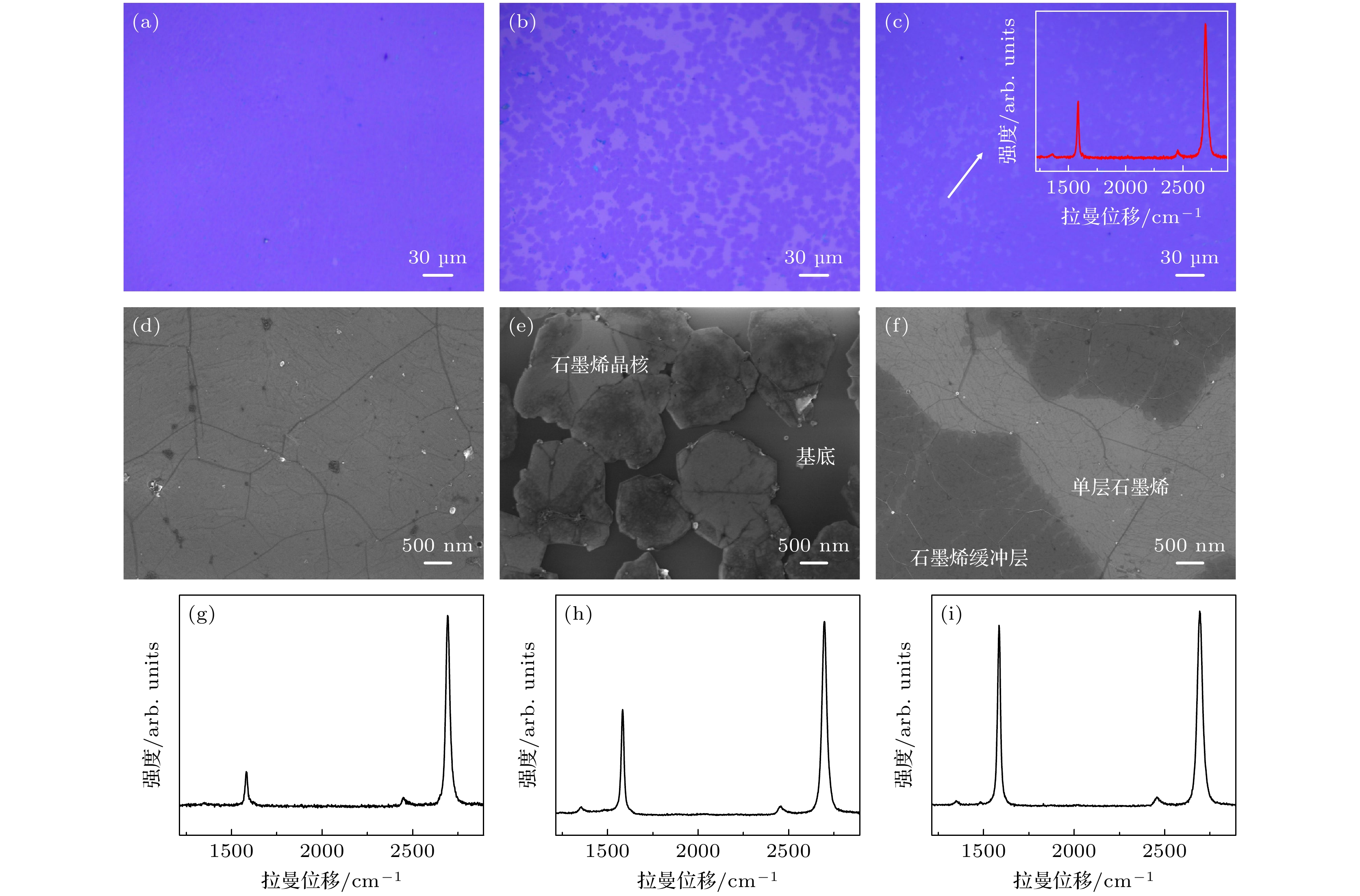
图 3 转移后的石墨烯. 光镜图 (a)单层石墨烯薄膜; (b)石墨烯岛; (c)有缓冲层石墨烯. 电镜图 (d)单层石墨烯薄膜; (e)石墨烯岛; (f)有缓冲层石墨烯. 拉曼光谱图 (g)单层石墨烯薄膜; (h)石墨烯岛; (i)有缓冲层石墨烯
Figure 3. Graphene after transferring. Optical microscope images of (a) single-layer grapheme, (b) graphene islands, (c) graphene with buffer layers. Scanning electron microscope images of (d) single-layer grapheme, (e) graphene islands, (f) graphene with buffer layers. Raman spectra images of (g) single-layer grapheme, (h) graphene islands, (i) graphene with buffer layers.
表 1 不同形貌石墨烯的CVD生长参数
Table 1. CVD growth parameters of graphene with different morphologies.
石墨烯形貌类型 生长温度/
℃甲烷浓度/
sccm氢气浓度/
sccm生长时间/
min单层石墨烯薄膜 1030 2 20 5 石墨烯岛 1030 2 30 5 有缓冲层石墨烯 1030 5 20 5 -
[1] Zhang Y B, Tan Y W, Stormer H L, Kim P 2005 Nature 438 201
 Google Scholar
[2] Prasher R 2010 Science 328 185
 Google Scholar
[3] Lee C G, Wei X D, Kysar J W, Hone J 2008 Science 321 385
 Google Scholar
[4] Novoselov K S, Fal′ko V I, Colombo L, Gellert P R, Schwab M G, Kim K 2012 Nature 490 192
 Google Scholar
[5] Chen Y C, Chen J, Li Z B 2023 Nanomaterials 13 2437
 Google Scholar
[6] Patra A, More M A, Late D J, Rout C S 2021 J. Mater. Chem. C 9 11059
 Google Scholar
[7] Shao X Y, Srinivasan A, Ang W K, Khursheed A 2018 Nat. Commun. 9 1288
 Google Scholar
[8] Yamaguchi H, Murakami K, Eda G, Fujita T, Guan P, Wang W H, Gong C, Boisse J, Miller S, Acik M, Cho K, Chabal Y J, Chen M W, Wakaya F, Takai M, Chhowalla M 2011 ACS Nano 5 4945
 Google Scholar
[9] Novoselov K S, Geim A K, Morozov S V, Jiang D, Zhang Y, Dubonos S V, Grigorieva I V, Firsov A A 2004 Science 306 666
 Google Scholar
[10] 陈浩, 彭同江, 刘波, 孙红娟, 雷德会 2017 物理学报 66 080701
 Google Scholar
Chen H, Peng T J, Liu B, Sun H J, Lie D H 2017 Acta Phys. Sin. 66 080701
 Google Scholar
[11] Berger C, Song Z, Li X, Wu X, Brown N, Naud C, Mayou D, Li T, Hass J, Marchenkov A N, Conrad E H, First P N, Heer W A D 2006 Science 312 1191
 Google Scholar
[12] Li X, Cai W, Colombo L, Ruoff R S 2009 Nano Lett. 9 4268
 Google Scholar
[13] Meng G D, Zhan F Z, She J Y, Xie J A, Zheng Q R, Cheng Y H, Yin Z Y 2023 Nanoscale 15 15994
 Google Scholar
[14] Xie J A, Meng G D, Chen B Y, Li Z, Yin Z Y, Cheng Y H 2022 ACS Appl. Mater. Interfaces 14 45716
 Google Scholar
[15] Regmi M, Chisholm M F, Eres G 2012 Carbon 50 134
 Google Scholar
[16] Liu W, Li H, Xu C, Khatami Y, Banerjee K 2011 Carbon 49 4122
 Google Scholar
[17] Deokar G, Avila J, Razado-Colambo I, Codron J L, Boyaval C, Galopin E, Asensio M C, Vignaud D 2015 Carbon 89 82
 Google Scholar
[18] Kleshch V I, Bandurin D A, Orekhov A S, Purcell S T, Obraztsov A N 2015 Appl. Surf. Sci. 357 1967
 Google Scholar
[19] 成桂霖, 杨健君, 全盛, 钟健, 于军胜 2022 真空科学与技术学报 42 290
Cheng G L, Yang J J, Quan S, Zhong J, Yu J S 2022 Vacuum Sci. Tech. 42 290
[20] Li Z B 2015 Ultramicroscopy 159 162
 Google Scholar
[21] 张晓波, 青芳竹, 李雪松 2019 物理学报 68 096801
 Google Scholar
Zhang X B, Qing F Z, Li X S 2019 Acta Phys. Sin. 68 096801
 Google Scholar
[22] Graf D, Molitor F, Ensslin K, Stampfer C, Jungen A, Hierold C, Wirtz L 2007 Nano Lett. 7 238
 Google Scholar
[23] Wang Y Y, Ni Z H, Yu T, Shen Z X, Wang H M, Wu Y H, Chen W, Shen Wee A T 2008 J. Phys. Chem. C 112 10637
 Google Scholar
[24] Fowler R H, Nordheim L 1928 Proc. R. Soc. Lond. A 119 173
 Google Scholar
[25] Zhang X, Wang L, Xin J, Yakobson B I, Ding F 2014 J. Am. Chem. Soc. 136 3040
 Google Scholar
[26] Lee S W, Lee S S, Yang E H 2009 Nanoscale Res. Lett. 4 1218
 Google Scholar
[27] Qian M, Feng T, Ding H, Lin L, Li H, Chen Y, Sun Z 2009 Nanotechnology 20 425702
 Google Scholar
[28] Liu J, Zeng B, Wu Z, Zhu J, Liu X 2010 Appl. Phys. Lett. 97 033109
 Google Scholar
[29] Xiao Z M, She J C, Deng S Z, Tang Z K, Li Z B, Lu J M, Xu N S 2010 ACS Nano 4 6332
 Google Scholar
[30] Tang S, Zhang Y, Zhao P, Zhan R, Chen J, Deng S 2021 Nanoscale 13 5234
 Google Scholar
Catalog
Metrics
- Abstract views: 5184
- PDF Downloads: 385
- Cited By: 0


 DownLoad:


