


-
Since the discovery of monolayer graphene, the novel physical properties of two-dimensional (2D) materials, particularly those with fewer layers that often exhibit unique properties different from bulk materials, have received significant attention. Therefore, accurately determining the layer number or obtaining the microscopic surface morphology is crucial in the laboratory fabrication and during device manufacturing. However, traditional detection methods have numerous drawbacks. There is an urgent need for a convenient, accurate, and non-destructive scientific method to characterize the layer number and surface microstructure of 2D materials. By combining the experimental setup of laser scanning photocurrent spectroscopy, we develop a polarization-modulated scanning optical microscope based on the principle of reflectance difference spectroscopy. By monitoring the reflectivity of the samples, we can observe changes in the reflection signal strength of MoS2 with different layer numbers. The intensity of the reflectance differential spectral signal reflects changes in the layer count within the sample. We can characterize the changes in the number of layers of 2D materials in a non-contact manner by using polarization-modulated scanning optical microscopy. Through the study of the reflectance differential spectra of two typical 2D layered materials, MoS2 and ReSe2, we find that our polarization-modulated scanning optical microscope system is also more sensitive to the characteristics of the stacking anisotropy of the 2D materials than the conventional reflection microscope. This indicates that our research contributes to a better understanding of the layer number characteristics and anisotropic properties of layered 2D materials. Furthermore, our research also provides a non-contact optical method to characterize the number of layers and optical anisotropy of two-dimensional layered material.
-
Keywords:
- reflectance anisotropy spectroscopy /
- microscopic imaging /
- optical anisotropy /
- two-dimensional materials
[1] Castro Neto A H, Guinea F, Peres N M R, Novoselov K S, Geim A K 2009 Rev. Mod. Phys. 81 109
 Google Scholar
[2] Geim A K, Novoselov K S 2007 Nat. Mater. 6 183
Google Scholar
[3] Geim A K, Grigorieva I V 2013 Nature 499 419
Google Scholar
[4] Butler S Z, Hollen S M, Cao L, Cui Y, Gupta J A, Gutierrez H R, Heinz T F, Hong S S, Huang J, Ismach A F, Johnston-Halperin E, Kuno M, Plashnitsa V V, Robinson R D, Ruoff R S, Salahuddin S, Shan J, Shi L, Spencer M G, Terrones M, Windl W, Goldberger J E 2013 ACS Nano 7 2898
Google Scholar
[5] Qiao J, Kong X H, Hu Z X, Yang F, Ji W 2014 Nat. Commun. 5 4475
Google Scholar
[6] Wang Q H, Kalantar-Zadeh K, Kis A, Coleman J N, Strano M S 2012 Nat. Nanotechnol. 7 699
Google Scholar
[7] Splendiani A, Sun L, Zhang Y B, Li T S, Kim J, Chim C Y, Galli G, Wang F 2010 Nano Lett. 10 1271
Google Scholar
[8] Mak K F, Lee C, Hone J, Shan J, Heinz T F 2010 Phys. Rev. Lett. 105 136805
Google Scholar
[9] Chhowalla M, Shin H S, Eda G, Li L J, Loh K P, Zhang H 2013 Nat. Chem. 5 263
Google Scholar
[10] Kim T, Kim D, Kim T, Kim H, Shin C 2022 Microsc. Microanal. 28 1604
Google Scholar
[11] Dong X C, Li H W, Yan Y T, Cheng H R, Zhang H X, Zhang Y C, Le T D, Wang K, Dong J, Jakobi M, Yetisen A K, Koch A W 2022 Adv. Theory Simul. 5 2200140
Google Scholar
[12] de Graaf S, Kooi B J 2022 2D Mater. 9 015009
Google Scholar
[13] Xiao Y P, Zheng W W, Yuan B, Wen C, Lanza M 2021 Cryst. Res. Technol. 56 2100056
Google Scholar
[14] Jin Y, Yu K 2021 J. Phys. D: Appl. Phys. 54 393001
Google Scholar
[15] Zhou X, Liu Y S, Hu X M, Fang L, Song Y M, Liu D M, Luo J B 2020 Nanotechnology 31 285710
Google Scholar
[16] Caplins B W, Holm J D, Keller R R 2019 Carbon 149 400
Google Scholar
[17] Liang F, Xu H J, Wu X, Wang C L, Luo C, Zhang J 2018 Chin. Phys. B 27 037802
Google Scholar
[18] Zhang X, Qiao X F, Shi W, Wu J B, Jiang D S, Tan P H 2015 Chem. Soc. Rev. 44 2757
Google Scholar
[19] Li X L, Qiao X F, Han W P, Lu Y, Tan Q H, Liu X L, Tan P H 2015 Nanoscale 7 8135
Google Scholar
[20] Lee K R, Youn J, Yoo S 2024 Nanophotonics 13 1417
Google Scholar
[21] Wang Q, Qin J, Xiao Y, Xu W, Ding L 2023 Electronics 12 864
Google Scholar
[22] Zou B, Zhou Y, Zhou Y, Wu Y Y, He Y, Wang X N, Yang J F, Zhang L H, Chen Y X, Zhou S, Guo H X, Sun H R 2022 Nano Res. 15 8470
Google Scholar
[23] Wang S Y, Chen G X, Guo Q Q, Huang K X, Zhang X L, Yan X Q, Liu Z B, Tian J G 2021 Nanoscale Adv. 3 3114
Google Scholar
[24] 乔晓粉, 李晓莉, 刘赫男, 石薇, 刘雪璐, 吴江滨, 谭平恒 2016 物理学报 65 136801
Google Scholar
Qiao X F, Li X L, Liu H N, Shi W, Liu X L, Wu J B, Tan P H 2016 Acta Phys. Sin. 65 136801
Google Scholar
[25] Jiang H, Shi H Y, Sun X D, Gao B 2018 Appl. Phys. Lett. 113 213105
Google Scholar
[26] Jiang H, Shi H Y, Sun X D, Gao B 2018 ACS Photonics 5 2509
Google Scholar
[27] Huang W, Yu J L, Liu Y, Peng Y, Wang L J, Liang P, Chen T S, Xu X G, Liu F Q, Chen Y H 2024 Chin. Phys. B 33 037801
Google Scholar
[28] Huang W, Liu Y, Zhu L P, Zheng X T, Li Y, Wu Q, Wang Y X, Wang X Q, Chen Y H 2016 Opt. Express 24 15059
Google Scholar
[29] Yu J L, Chen Y H, Cheng S Y, Lai Y F 2013 Appl. Opt. 52 1035
Google Scholar
[30] Wu S J, Chen Y H, Yu J L, Gao H S, Jiang C Y, Huang J L, Zhang Y H, Wei Y, Ma W Q 2013 Nanoscale Res. Lett. 8 298
Google Scholar
[31] Kim E D, Majumdar A, Kim H, Petroff P, Vuckovic J 2010 Appl. Phys. Lett. 97 053111
Google Scholar
[32] Aspnes D E, Harbison J P, Studna A A, Florez L T 1987 Phys. Rev. Lett. 59 1687
Google Scholar
[33] 沈万福 2019 博士论文(天津: 天津大学)
Shen W F 2019 Ph. D. Dissertation (Tianjin: Tianjin University
[34] 蒋虎 2019 博士论文 (哈尔滨: 哈尔滨工业大学)
Jiang H 2019 Ph. D. Dissertation (Haerbin: Harbin Institute of Technology
[35] Shi Y F, Wang L L, Q X F, Li S, Liu Y, Li X L, Zhao X H 2020 Nanoscale Res. Lett. 15 43
Google Scholar
[36] Ermolaev G A, Voronin K V, Toksumakov A N, Grudinin D V, Fradkin I M, Mazitov A, Slavich A S, Tatmyshevskiy M K, Yakubovsky D I, Solovey V R, Kirtaev R V 2024 Nat. Commun. 15 1552
Google Scholar
-
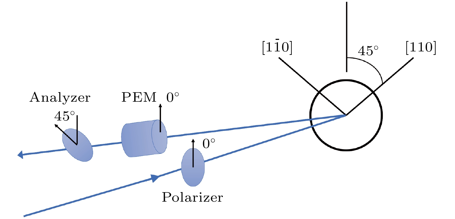
图 1 RDS的实验原理图
Figure 1. Experimental schematic diagram of RDS.
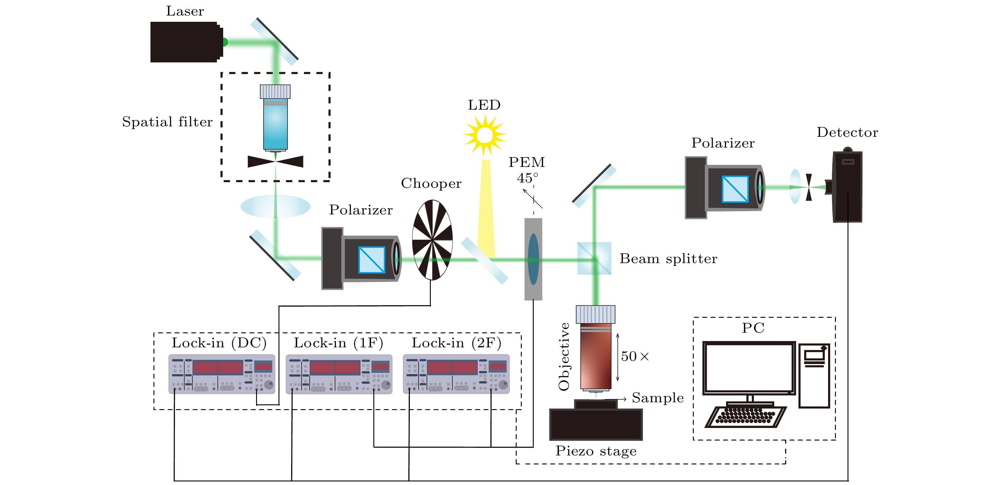
图 2 偏振调制扫描光学显微镜光路图
Figure 2. Polarization-modulated scanning optical microscope optical path diagram.
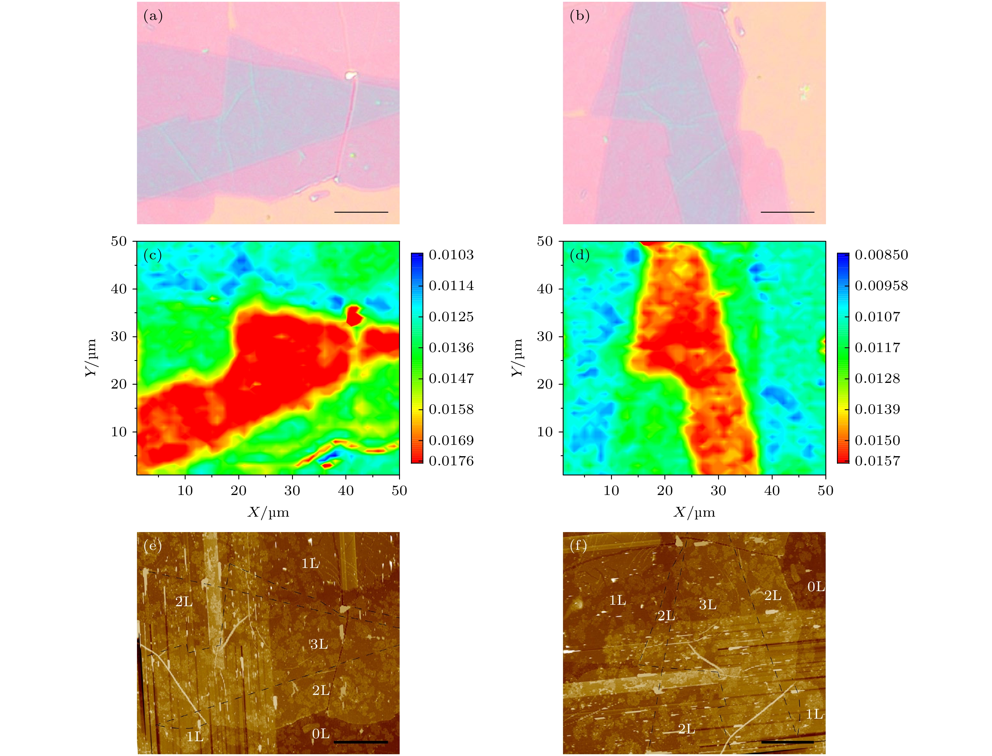
图 3 MoS2光学显微镜照片及反射谱二维图像 (a) 0°的MoS2光学显微镜照片; (b) 90°的MoS2光学显微镜照片; (c), (d)分别为对应的MoS2反射谱(DC信号)的二维图像; (e), (f) 分别为对应的MoS2 AFM图像. 黑线为标度尺, 大小为10 μm
Figure 3. Optical microscope image and reflectance spectrum two-dimensional (2D) image of MoS2: (a) Optical microscope photographs of MoS2 at 0°; (b) optical microscope photographs of MoS2 at 90°; (c), (d) 2D images of the corresponding MoS2 reflection spectra (DC signals), respectively; (e), (f) AFM images of the corresponding MoS2. The black line is a scale with a size of 10 μm.
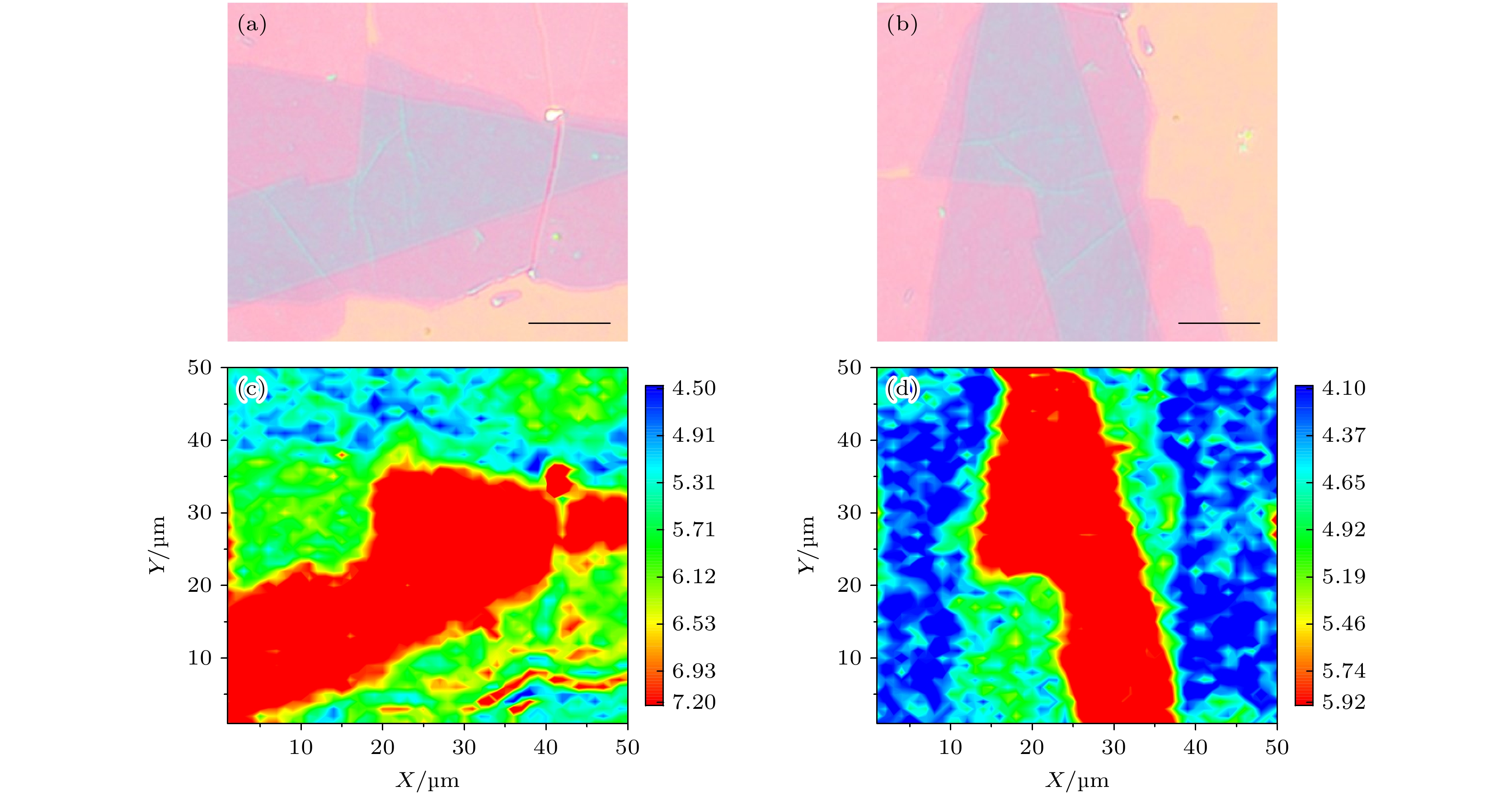
图 4 MoS2光学显微镜照片及反射差分谱二维图像 (a) 0°的MoS2光学显微镜照片; (b) 90°的MoS2光学显微镜照片; (c), (d)分别为对应的MoS2 各向异性信号(RDS信号)的二维图像. 黑线为标度尺, 大小为10 μm
Figure 4. Optical microscope image and reflectance differential spectrum 2D Image of MoS2: (a) Optical microscope photographs of MoS2 at 0°; (b) optical microscope photographs of MoS2 at 90°; (c), (d) 2D images of the corresponding MoS2 anisotropic signal (RDS signal), respectively. The black line is a scale with a size of 10 μm.
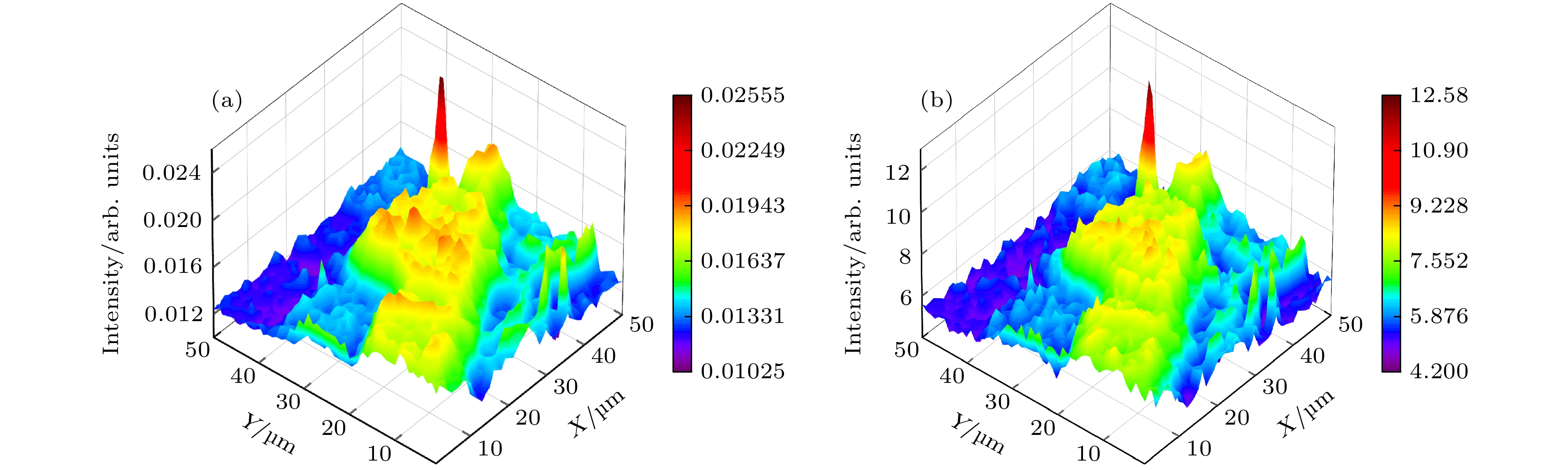
图 5 MoS2反射谱与反射差分谱的空间映射图 (a)不同层数MoS2的反射谱的强度空间映射图; (b)不同层数MoS2的RDS信号强度空间映射图
Figure 5. Spatial mapping of MoS2 reflectance spectrum and reflectance differential spectrum: (a) Intensity spatial mapping of reflection spectra for different layers of MoS2; (b) intensity spatial mapping of RDS signal for different layers of MoS2.
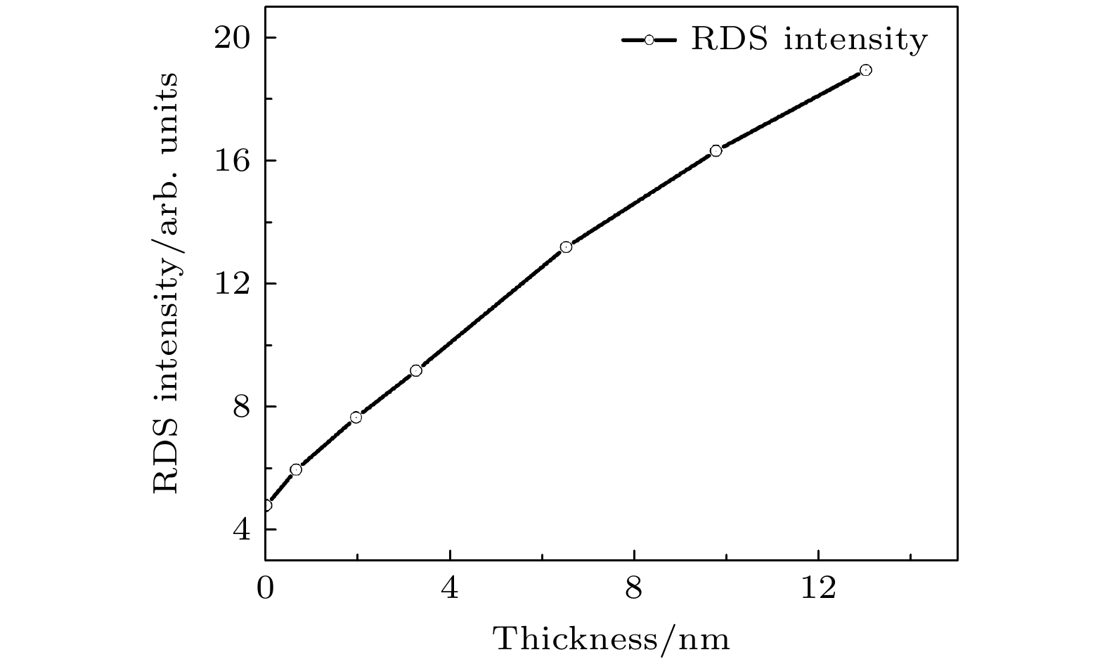
图 6 不同层数MoS2的RDS信号强度随层数的变化
Figure 6. Relationship between the RDS signal intensity of MoS2 and the number of layers.
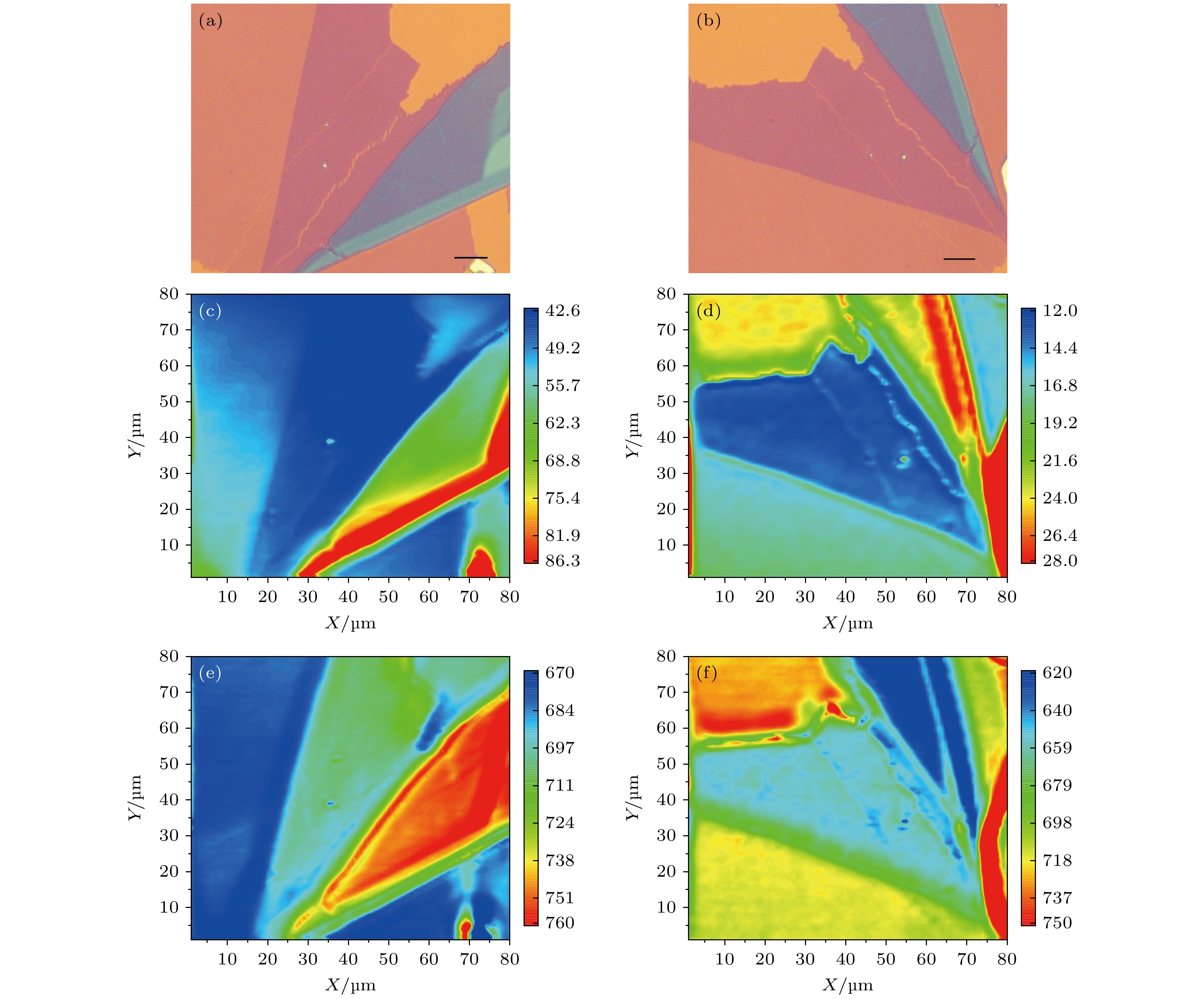
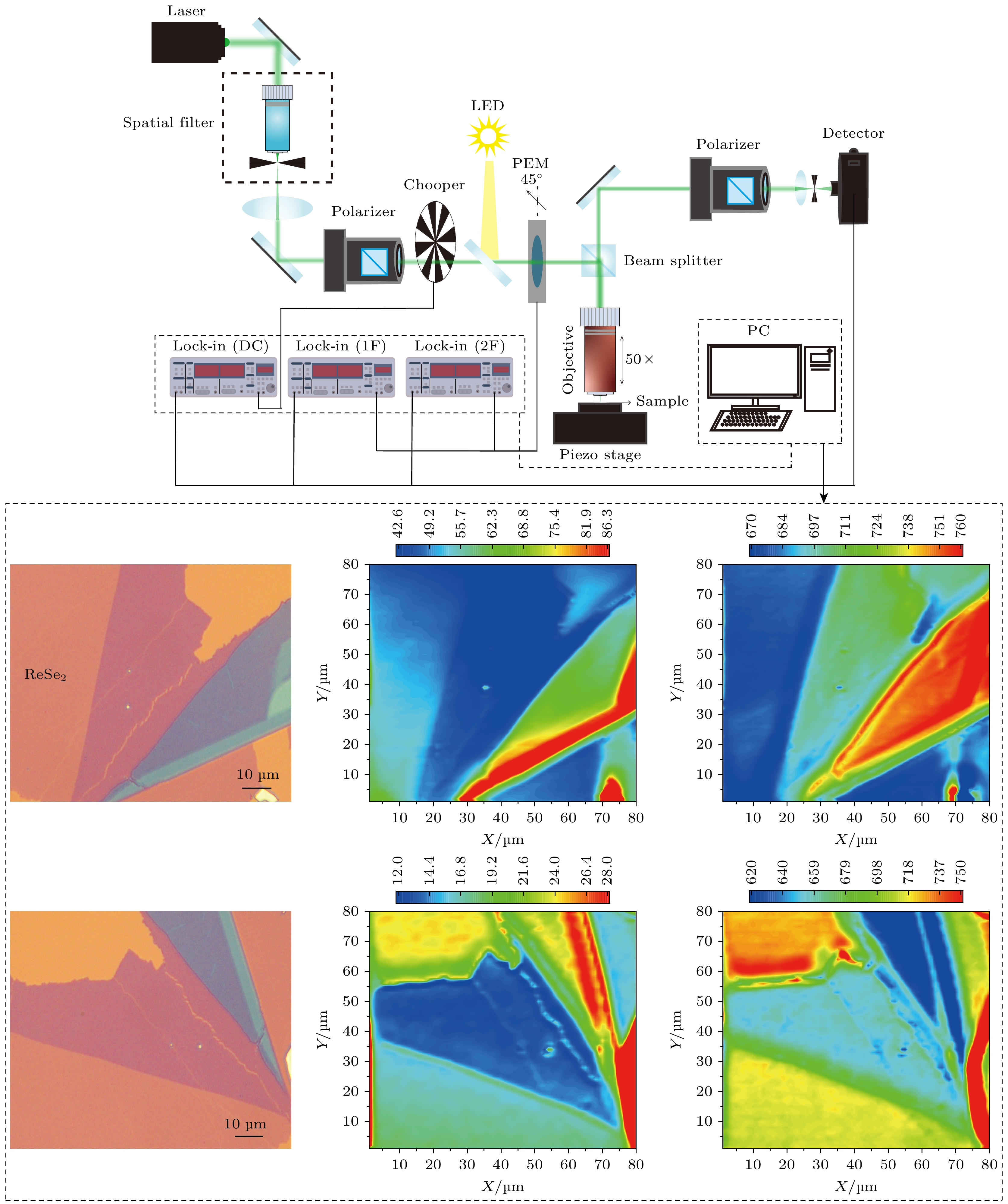
图 7 ReSe2的光学显微镜照片、DC信号的二维图像及RDS信号的二维图像 (a) 0° 的ReSe2的光学显微镜照片; (c) 0°的ReSe2的DC信号的二维图像; (e) 0°的ReSe2的RDS信号的二维图像; (b) 90°的ReSe2的光学显微镜照片; (d) 90°的ReSe2的DC信号的二维图像; (f) 90°的ReSe2的RDS信号的二维图像. 黑线为标度尺, 大小为10 μm
Figure 7. Optical microscope image of ReSe2, 2D image of DC signal, and 2D image of RDS signal: (a) Optical microscope photographs of ReSe2 at 0°; (c) 2D image of DC signal of ReSe2 at 0°; (e) 2D image of RDS signal of ReSe2 at 0°; (b) optical microscope photographs of ReSe2 at 90°; (d) 2D image of DC signal of ReSe2 at 90°; (f) 2D image of RDS signal of ReSe2 at 90°. The black line is a scale with a size of 10 μm.
-
[1] Castro Neto A H, Guinea F, Peres N M R, Novoselov K S, Geim A K 2009 Rev. Mod. Phys. 81 109
Google Scholar
[2] Geim A K, Novoselov K S 2007 Nat. Mater. 6 183
Google Scholar
[3] Geim A K, Grigorieva I V 2013 Nature 499 419
Google Scholar
[4] Butler S Z, Hollen S M, Cao L, Cui Y, Gupta J A, Gutierrez H R, Heinz T F, Hong S S, Huang J, Ismach A F, Johnston-Halperin E, Kuno M, Plashnitsa V V, Robinson R D, Ruoff R S, Salahuddin S, Shan J, Shi L, Spencer M G, Terrones M, Windl W, Goldberger J E 2013 ACS Nano 7 2898
Google Scholar
[5] Qiao J, Kong X H, Hu Z X, Yang F, Ji W 2014 Nat. Commun. 5 4475
Google Scholar
[6] Wang Q H, Kalantar-Zadeh K, Kis A, Coleman J N, Strano M S 2012 Nat. Nanotechnol. 7 699
Google Scholar
[7] Splendiani A, Sun L, Zhang Y B, Li T S, Kim J, Chim C Y, Galli G, Wang F 2010 Nano Lett. 10 1271
Google Scholar
[8] Mak K F, Lee C, Hone J, Shan J, Heinz T F 2010 Phys. Rev. Lett. 105 136805
Google Scholar
[9] Chhowalla M, Shin H S, Eda G, Li L J, Loh K P, Zhang H 2013 Nat. Chem. 5 263
Google Scholar
[10] Kim T, Kim D, Kim T, Kim H, Shin C 2022 Microsc. Microanal. 28 1604
Google Scholar
[11] Dong X C, Li H W, Yan Y T, Cheng H R, Zhang H X, Zhang Y C, Le T D, Wang K, Dong J, Jakobi M, Yetisen A K, Koch A W 2022 Adv. Theory Simul. 5 2200140
Google Scholar
[12] de Graaf S, Kooi B J 2022 2D Mater. 9 015009
Google Scholar
[13] Xiao Y P, Zheng W W, Yuan B, Wen C, Lanza M 2021 Cryst. Res. Technol. 56 2100056
Google Scholar
[14] Jin Y, Yu K 2021 J. Phys. D: Appl. Phys. 54 393001
Google Scholar
[15] Zhou X, Liu Y S, Hu X M, Fang L, Song Y M, Liu D M, Luo J B 2020 Nanotechnology 31 285710
Google Scholar
[16] Caplins B W, Holm J D, Keller R R 2019 Carbon 149 400
Google Scholar
[17] Liang F, Xu H J, Wu X, Wang C L, Luo C, Zhang J 2018 Chin. Phys. B 27 037802
Google Scholar
[18] Zhang X, Qiao X F, Shi W, Wu J B, Jiang D S, Tan P H 2015 Chem. Soc. Rev. 44 2757
Google Scholar
[19] Li X L, Qiao X F, Han W P, Lu Y, Tan Q H, Liu X L, Tan P H 2015 Nanoscale 7 8135
Google Scholar
[20] Lee K R, Youn J, Yoo S 2024 Nanophotonics 13 1417
Google Scholar
[21] Wang Q, Qin J, Xiao Y, Xu W, Ding L 2023 Electronics 12 864
Google Scholar
[22] Zou B, Zhou Y, Zhou Y, Wu Y Y, He Y, Wang X N, Yang J F, Zhang L H, Chen Y X, Zhou S, Guo H X, Sun H R 2022 Nano Res. 15 8470
Google Scholar
[23] Wang S Y, Chen G X, Guo Q Q, Huang K X, Zhang X L, Yan X Q, Liu Z B, Tian J G 2021 Nanoscale Adv. 3 3114
Google Scholar
[24] 乔晓粉, 李晓莉, 刘赫男, 石薇, 刘雪璐, 吴江滨, 谭平恒 2016 物理学报 65 136801
Google Scholar
Qiao X F, Li X L, Liu H N, Shi W, Liu X L, Wu J B, Tan P H 2016 Acta Phys. Sin. 65 136801
Google Scholar
[25] Jiang H, Shi H Y, Sun X D, Gao B 2018 Appl. Phys. Lett. 113 213105
Google Scholar
[26] Jiang H, Shi H Y, Sun X D, Gao B 2018 ACS Photonics 5 2509
Google Scholar
[27] Huang W, Yu J L, Liu Y, Peng Y, Wang L J, Liang P, Chen T S, Xu X G, Liu F Q, Chen Y H 2024 Chin. Phys. B 33 037801
Google Scholar
[28] Huang W, Liu Y, Zhu L P, Zheng X T, Li Y, Wu Q, Wang Y X, Wang X Q, Chen Y H 2016 Opt. Express 24 15059
Google Scholar
[29] Yu J L, Chen Y H, Cheng S Y, Lai Y F 2013 Appl. Opt. 52 1035
Google Scholar
[30] Wu S J, Chen Y H, Yu J L, Gao H S, Jiang C Y, Huang J L, Zhang Y H, Wei Y, Ma W Q 2013 Nanoscale Res. Lett. 8 298
Google Scholar
[31] Kim E D, Majumdar A, Kim H, Petroff P, Vuckovic J 2010 Appl. Phys. Lett. 97 053111
Google Scholar
[32] Aspnes D E, Harbison J P, Studna A A, Florez L T 1987 Phys. Rev. Lett. 59 1687
Google Scholar
[33] 沈万福 2019 博士论文(天津: 天津大学)
Shen W F 2019 Ph. D. Dissertation (Tianjin: Tianjin University
[34] 蒋虎 2019 博士论文 (哈尔滨: 哈尔滨工业大学)
Jiang H 2019 Ph. D. Dissertation (Haerbin: Harbin Institute of Technology
[35] Shi Y F, Wang L L, Q X F, Li S, Liu Y, Li X L, Zhao X H 2020 Nanoscale Res. Lett. 15 43
Google Scholar
[36] Ermolaev G A, Voronin K V, Toksumakov A N, Grudinin D V, Fradkin I M, Mazitov A, Slavich A S, Tatmyshevskiy M K, Yakubovsky D I, Solovey V R, Kirtaev R V 2024 Nat. Commun. 15 1552
Google Scholar

 DownLoad:
Catalog
Metrics
- Abstract views: 4514
- PDF Downloads: 77
- Cited By: 0
