


-
Higher requirements for the performances of thin films need to be fulfilled in the rapid development of integrated circuit technology, due to the more complicate structure and smaller size of chips. In plasma-enhanced chemical vapor deposition , high-density and high-performance thin films can be deposited at low temperature, compared with traditional chemical vapor deposition. In this work, a two-dimensional fluid/MC model coupled with the deposition module is used to describe the capacitively coupled SiH4/N2O/Ar discharges as well as the deposition processes, focusing on the influences of the radial position, gas ratio and gas pressure on the deposition of silicon oxide films. The results show that the edge effect which leads the plasma density to rise near the electrode edges gives rise to the non-uniform deposition rate along the radial direction. It is also found that the more N2O and less Ar content in the gas mixture, as well as an increased gas pressure will improve this uniformity. However, an excessive deposition rate will lead to a series of undesirable phenomena, such as “key hole structure”, vacancies and excessive impurities in films. These problems are also troublesome in the microelectronics manufacture processes. More detailed investigation into the deposition mechanism can be expected in the future .
[1] Nam T, Lee H, Choi T, et al. 2019 Appl. Surf. Sci. 485 381
 Google Scholar
[2] Beynet J, Wong P, Miller A, et al. 2009 Proceedings of SPIE - The International Society for Optical Engineering 7520
[3] Lieberman M A, Lichtenberg A J 2005 Principles of Plasma Discharges and Materials Processing (New York: Wiley)
[4] Wuu D, Lo W, Chang L, Horng R 2004 Thin Solid Films 468 105
Google Scholar
[5] Jeong C H, Lee J H, Lim J T, Gil Cho N, Moon C H, Yeom G Y 2005 Jpn. J. Appl. Phys. 44 1022
Google Scholar
[6] Courtney C H, Smith B C, Lamb H H 1998 J. Electrochem. Soc. 145 3957
Google Scholar
[7] Yanguas-Gil A 2017 Growth and Transport in Nanostructured Materials: Reactive Transport in PVD, CVD and ALD (Berlin: Springer)
[8] Alvisi M, De Nunzio G, Di Giulio M, Ferrara M C, Perrone M R, Protopapa L, Vasanelli L 1999 Appl. Opt. 38 1237
Google Scholar
[9] Putkonen M, Bosund M, Ylivaara O M, et al. 2014 Thin Solid Films 558 93
Google Scholar
[10] Özkol E, Procel P, Zhao Y, et al. 2019 Phys. Status Solidi (RRL) Rapid Res. Lett. 14
[11] Pai P, Chao S S, Takagi Y, Lucovsky G 1986 J. Vac. Sci. Technol. A 4 689
Google Scholar
[12] Kushner M J 1993 J. Appl. Phys. 74 6538
Google Scholar
[13] Barron A R 2013 Chemistry of Electronic Materials. (Houston: Rice University) pp1–359
[14] Liu X, Ge J, Yang Y, Song Y, Ren T 2014 Plasma Sci. Technol. 16 385
Google Scholar
[15] Xu Q, Li Y X, Li X N, Wang J B, Yang F, Yang Y 2017 Modern Phys. Lett. B 31 1750055
Google Scholar
[16] Liu R Q, Liu Y, Jia W Z, Zhou Y W 2017 Phys. Plasmas 24 013517
Google Scholar
[17] 贾文柱 2018 博士学位论文 (大连: 大连理工大学)
Jia W Z 2018 Ph. D Dissertation (Dalian: Dalian University of Technology) (in Chinese)
[18] Cheng C C, Guinn K V, Donnelly V M, Herman I P 1994 J. Vac. Sci. Technol. A 12 2630
Google Scholar
[19] Abrams C F, Graves D B 1999 J. Appl. Phys. 86 2263
Google Scholar
[20] Lu Y, Kobayashi A, Kondo, H, Ishikawa K, Sekine M, Hori M 2014 Jpn. J. Appl. Phys. 53 010305
Google Scholar
[21] Tinck S, W Boullart, A Bogaerts 2009 J. Phys. D Appl. Phys. 86 095204
Google Scholar
[22] Qu C, Sakiyama Y, Agarwal P, Kushner M J 2021 J. Vac. Sci. Technol. A 39 052403
Google Scholar
[23] 张赛谦 2018 博士学位论文 (大连: 大连理工大学)
Zhang S Q 2018 Ph. D Dissertation (Dalian: Dalian University of Technology) (in Chinese)
[24] Date L, Radouane K, Despax B, Yousfi M, Caquineau H and Hennad A 1999 J. Phys. D Appl. Phys. 32 1478
Google Scholar
-
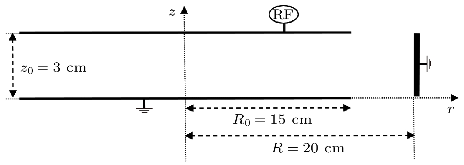
图 1 放电腔室结构示意图
Figure 1. Chamber structure of discharge.
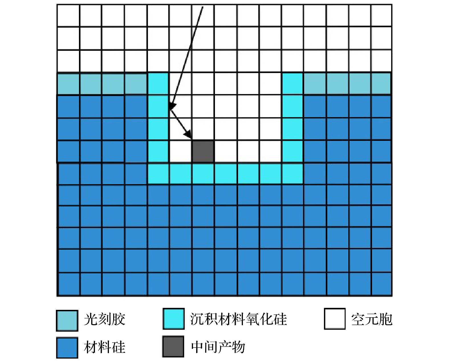
图 2 元胞法网格划分和属性分配示意图
Figure 2. Schematic diagram of cellular grid division and attribute allocation.
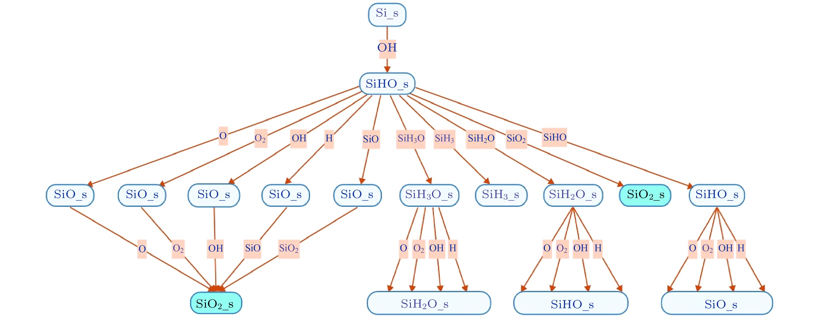
图 3 沉积模块考虑的表面反应过程示意图
Figure 3. Schematic diagram of the surface reaction processes considered by the deposition module.
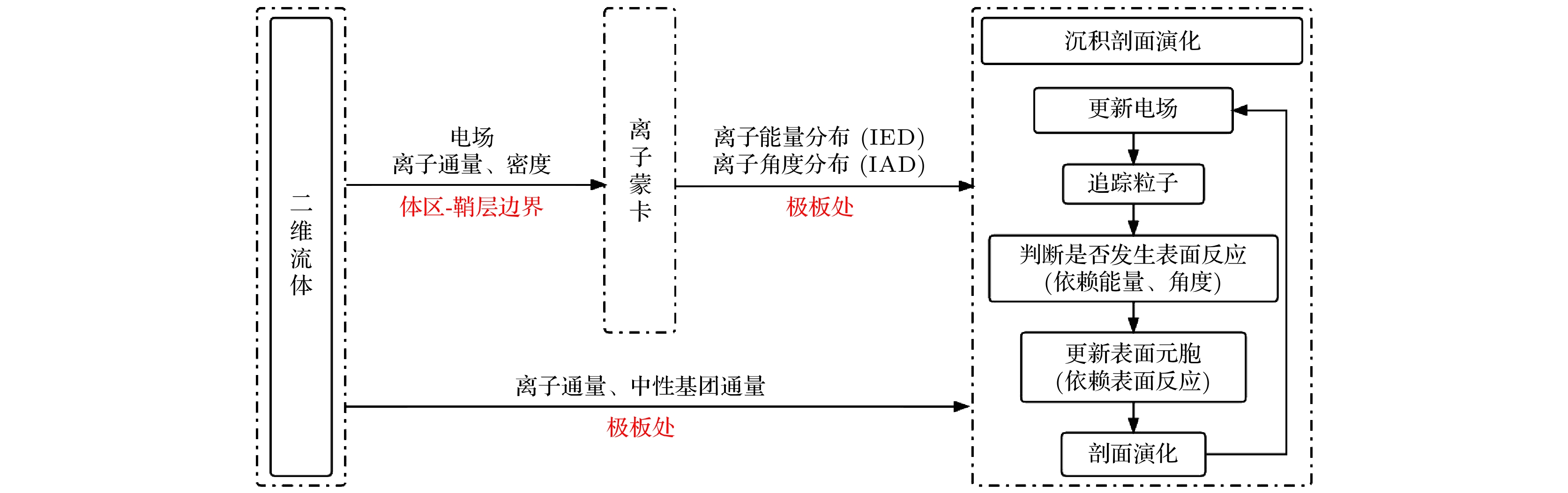
图 4 2D-fluid模块/IMC模块/沉积剖面演化模块信息传输示意图
Figure 4. Schematic diagram of 2D-fluid module/MC module/trench module information transmission.
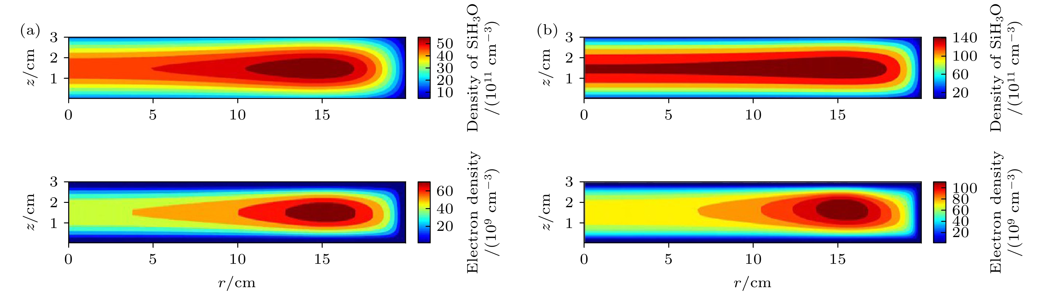
图 5 在(a) 1 Torr (1 Torr ≈ 133 Pa)和(b) 2 Torr气压下的射频周期平均中性基团SiH3O密度和电子密度的空间分布. 放电气体密度比SiH4/N2O/Ar = 2∶8∶90, 放电频率
$f=13.56\text{ MHz}$ , 电压${V}_{\mathrm{s}}=50\text{ V}$ Figure 5. Spatial density distributions of the neutral particle SiH3O and electron at different pressures, (a) 1 Torr (1 Torr ≈ 133 Pa) and (b) 2 Torr. The discharge gas density ratio is SiH4/N2O/Ar = 2∶8∶90, discharge frequency
$f=13.56\text{ MHz}$ , voltage${V}_{\mathrm{s}}=50\text{ V}$ 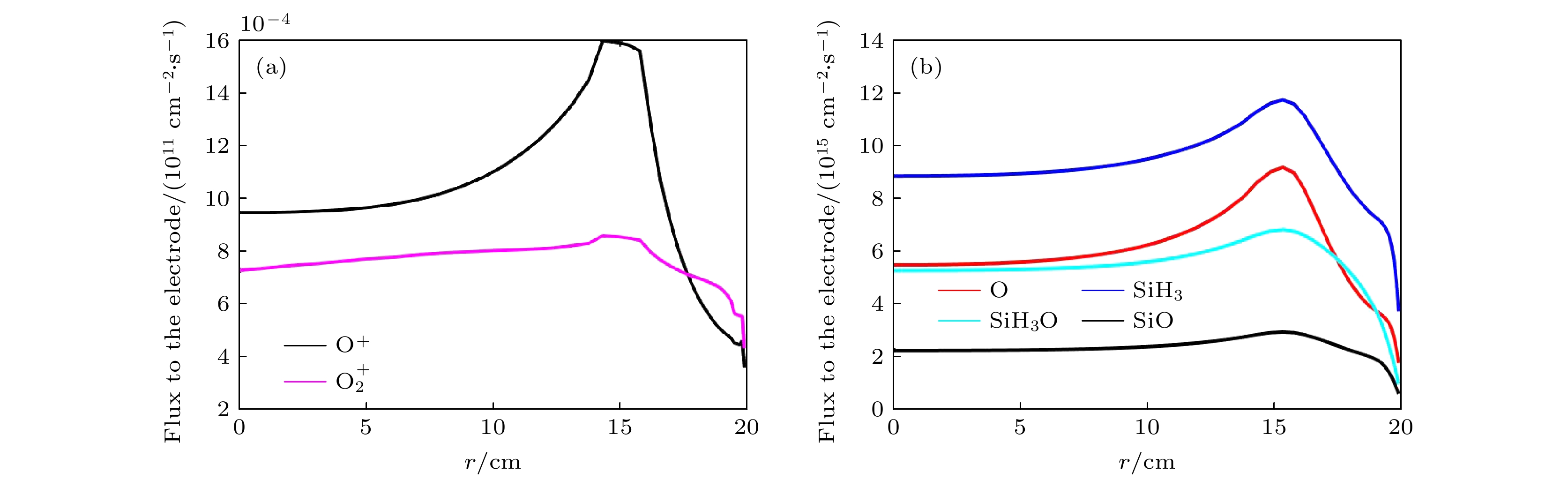
图 6 (a) 达到接地极板的离子通量随径向分布; (b) 达到接地极板的中性基团通量随径向分布. 放电气压2 Torr, 气体密度比SiH4/N2O/Ar = 2∶8∶90, 放电频率
$f=13.56\text{ MHz}$ , 电压${V}_{{{{\rm{s}}}}}=50\text{ V}$ Figure 6. Radial flux distributions of (a) ions (
$\rm O_2^+ $ , O+) and (b) neutral particles (O, SiH3O, SiH3, SiO) on the grounded electrode. The discharge pressure is 2 Torr. The gas density ratio is SiH4/N2O/Ar = 2∶8∶90, discharge frequency$f=13.56\text{ MHz}$ , voltage${V}_{{\rm{s}}}=50\text{ V}$ 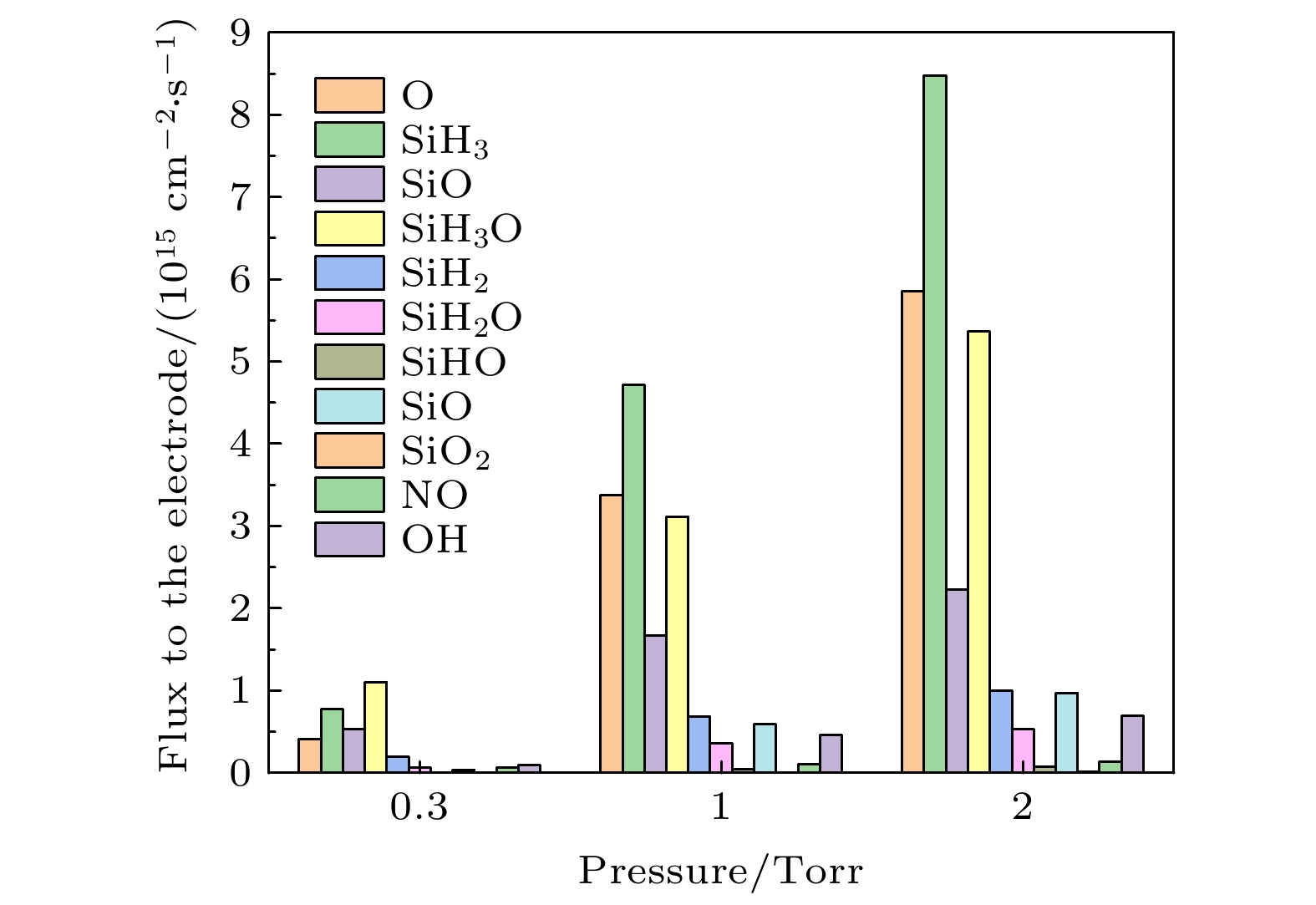
图 7 在不同气压下中性基团达到接地极板
$r=1\text{ cm}$ 的中性粒子通量. 放电气体密度比SiH4/N2O/Ar = 2∶8∶90, 放电频率$f=13.56\text{ MHz}$ , 电压${V}_{\mathrm{s}}=50\text{ V}$ Figure 7. Fluxes of neutral particles to the grounded electrode
$r=1\;\mathrm{ }\mathrm{c}\mathrm{m}$ at different pressures. The gas density ratio SiH4/N2O/Ar = 2∶8∶90, discharge frequency$f=13.56\text{ MHz}$ , voltage${V}_{\mathrm{s}}=50\text{ V}$ 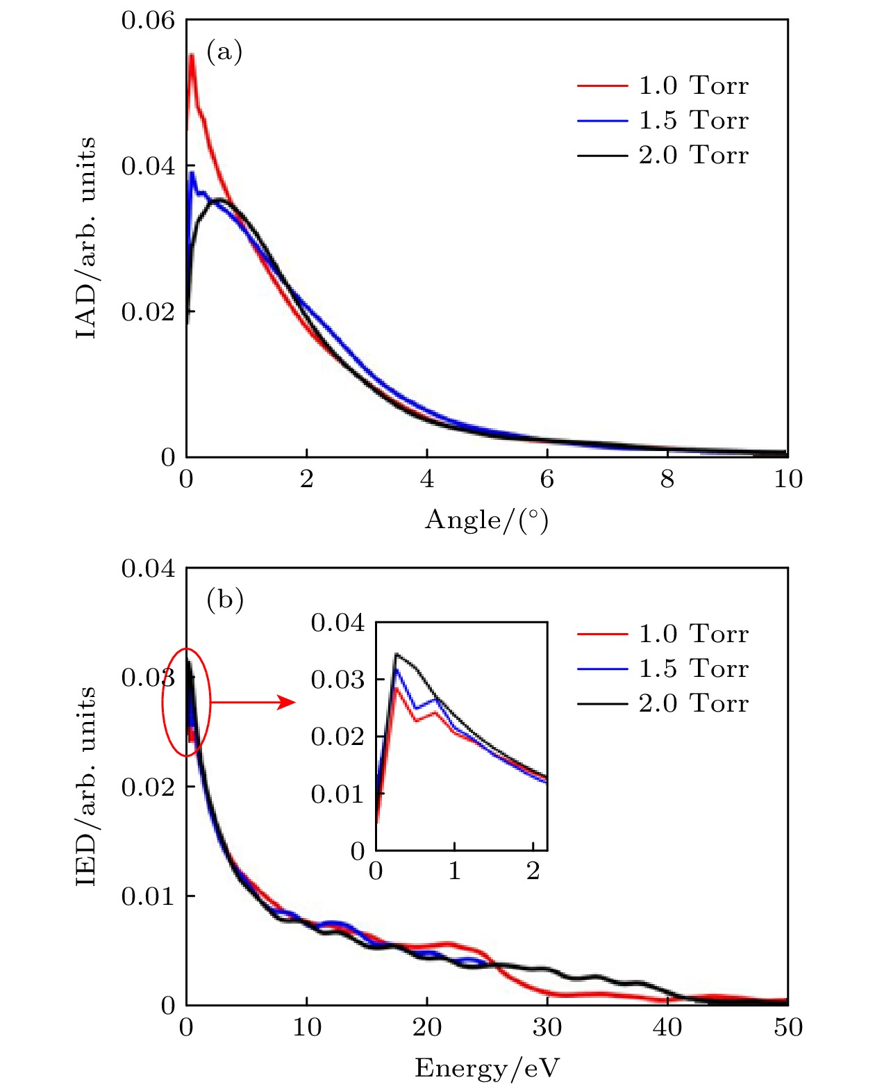
图 8 不同气压下接地极板
$r=1\text{ cm}$ 处的(a)Ar+离子角度分布(IAD) 和(b)Ar+离子能量分布(IED). 放电气体密度比SiH4/N2O/Ar = 2∶8∶90, 放电频率$f=13.56\text{ MHz}$ , 电压${V}_{\mathrm{s}}=50\text{ V}$ Figure 8. (a) Ion angle distributions (IADs) and (b) ion energy distributions (IEDs) of Ar+ at different pressures, at the grounded electrode
$r=1\text{ cm}$ . The discharge gas density ratio is SiH4/N2O/Ar = 2∶8∶90, discharge frequency$f=13.56\text{ MHz}$ , voltage${V}_{\mathrm{s}}=50\text{ V}$ 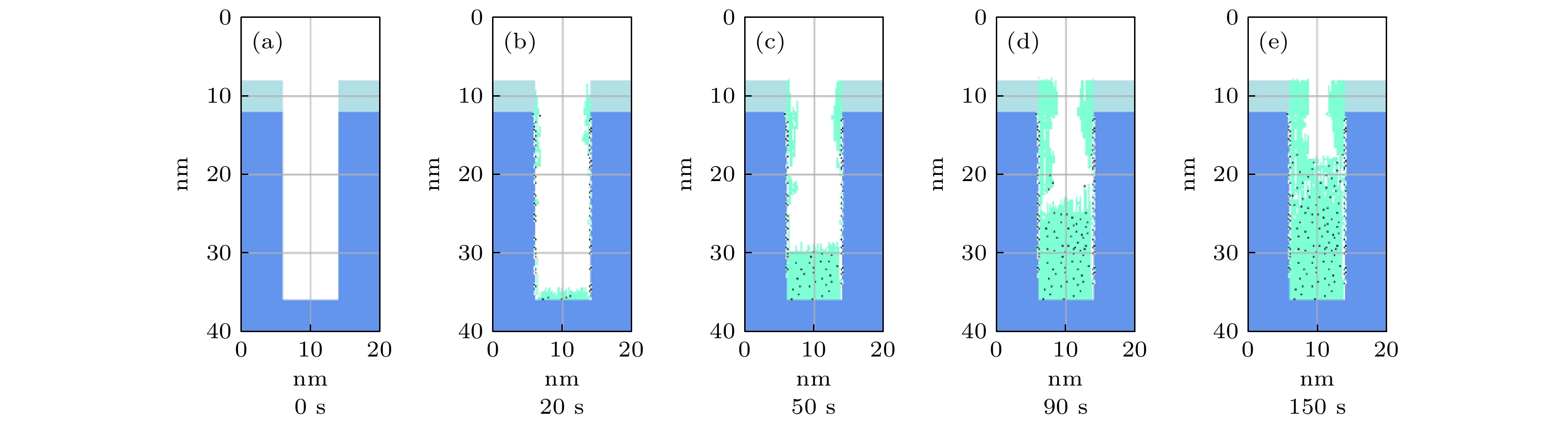
图 9 接地极板表面
$r=1\;\mathrm{c}\mathrm{m}$ 处的槽结构中沉积剖面随时间演化图. 放电气压2 Torr, 气体密度比SiH4/N2O/Ar = 2∶8∶90, 放电频率$f=13.56\text{ MHz}$ , 电压${V}_{\mathrm{s}}=50\text{ V}$ Figure 9. Temporal evolution of thin film profiles deposited in trench structure (depth-width ratio 3/1), at the grounded electrode
$r=1\;\mathrm{ }\mathrm{c}\mathrm{m}$ . The discharge pressure is 2 Torr, gas density ratio SiH4/N2O/Ar = 2∶8∶90, discharge frequency$f=13.56\text{ MHz}$ , voltage${V}_{\mathrm{s}}=50\text{ V}$ 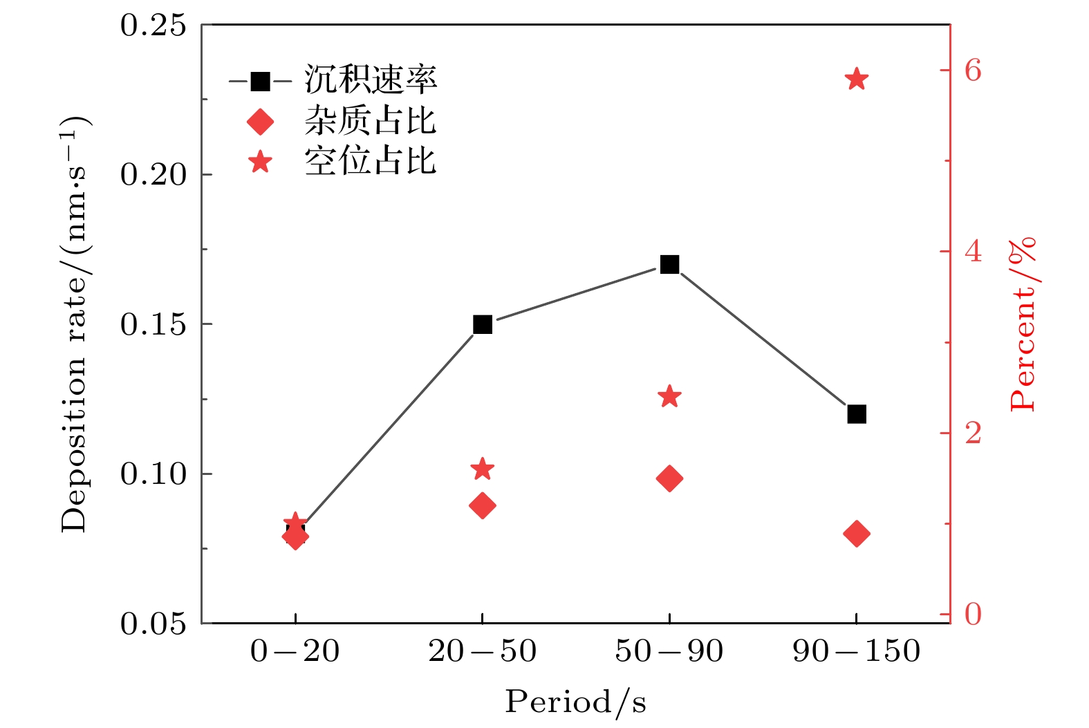
图 10 接地极板表面
$r=1\text{ cm}$ 处, 不同时刻的薄膜沉积速率、杂质占比和空位占比. 放电气压2 Torr, 气体密度比SiH4/N2O/Ar = 2∶8∶90, 放电频率$f$ = 13.56 MHz, 电压${V}_{\mathrm{s}}= 50\;\mathrm{ }\mathrm{V}$ Figure 10. Deposition rate and the proportions of impurities and vacancies at different periods, at the grounded electrode
$r=1\;\mathrm{ }\mathrm{c}\mathrm{m}$ . The discharge pressure is 2 Torr, gas density ratio SiH4/N2O/Ar = 2∶8∶90, discharge frequency$f=13.56\text{ MHz}$ , voltage Vs = 50 V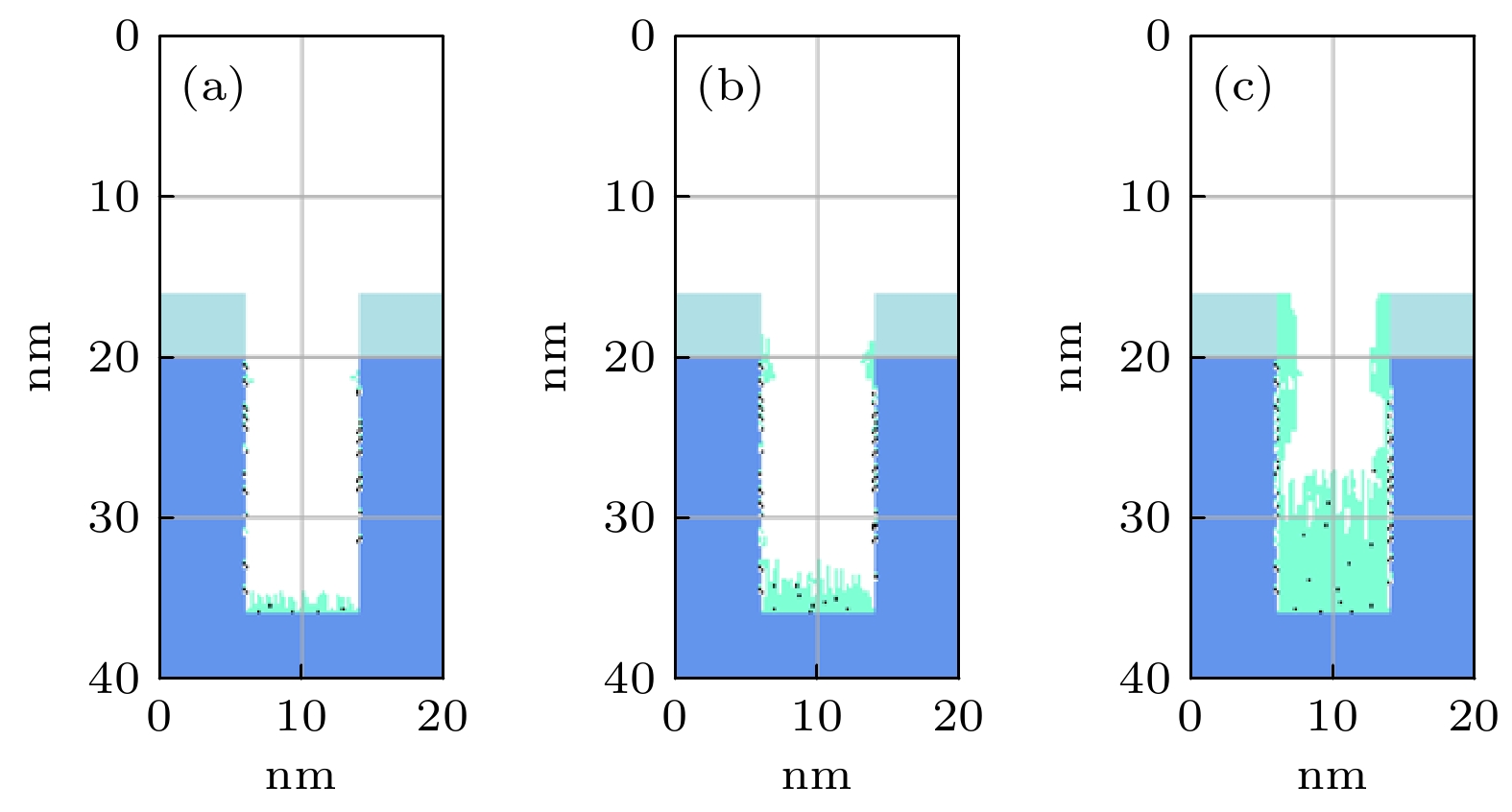
图 11 不同气压下沉积50 s接地极板表面
$r=1\;\mathrm{c}\mathrm{m}$ 处槽结构中沉积的薄膜剖面 (a) 0.3 Torr; (b) 1.0 Torr; (c) 2.0 Torr. 放电气体密度比SiH4/N2O/Ar = 2∶8∶90, 放电频率$f=13.56\text{ MHz}$ , 电压${V}_{\mathrm{s}}=50\text{ V}$ Figure 11. Profiles formed after deposition time(50 s) for different pressures: (a) 0.3 Torr, (b) 1.0 Torr, (c) 2.0 Torr, at
$r=1\;\mathrm{c}\mathrm{m}$ . The discharge gas density ratio is SiH4/N2O/Ar = 2∶8∶90, discharge frequency$f=13.56\text{ MHz}$ , voltage${V}_{\mathrm{s}}= $ $ 50\text{ V}$ 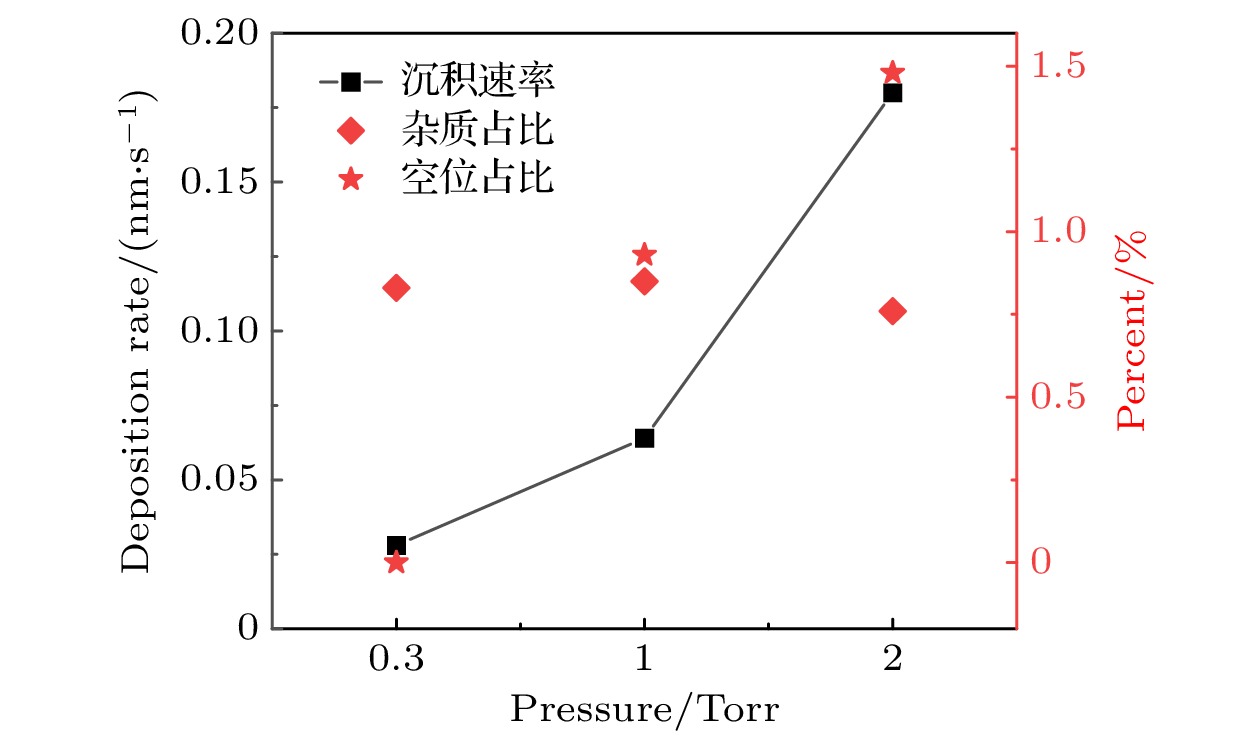
图 12 在接地极板表面
$r=1\;\mathrm{ }\mathrm{c}\mathrm{m}$ 处, 不同气压下0—50 s期间的薄膜沉积速率、杂质占比和空位占比. 放电气体密度比SiH4/N2O/Ar = 2∶8∶90, 放电频率$f= 13.56\text{ MHz}$ , 电压${V}_{\mathrm{s}}=50\text{ V}$ Figure 12. Deposition rate and the proportions of impurities and vacancies during deposition period (0–50 s) with different pressures, at the grounded electrode
$r=1\;\mathrm{ }\mathrm{c}\mathrm{m}$ . The discharge gas density ratio is SiH4/N2O/Ar = 2∶8∶90, discharge frequency$f=13.56\text{ MHz}$ , voltage${V}_{\mathrm{s}}=50\text{ V}$ 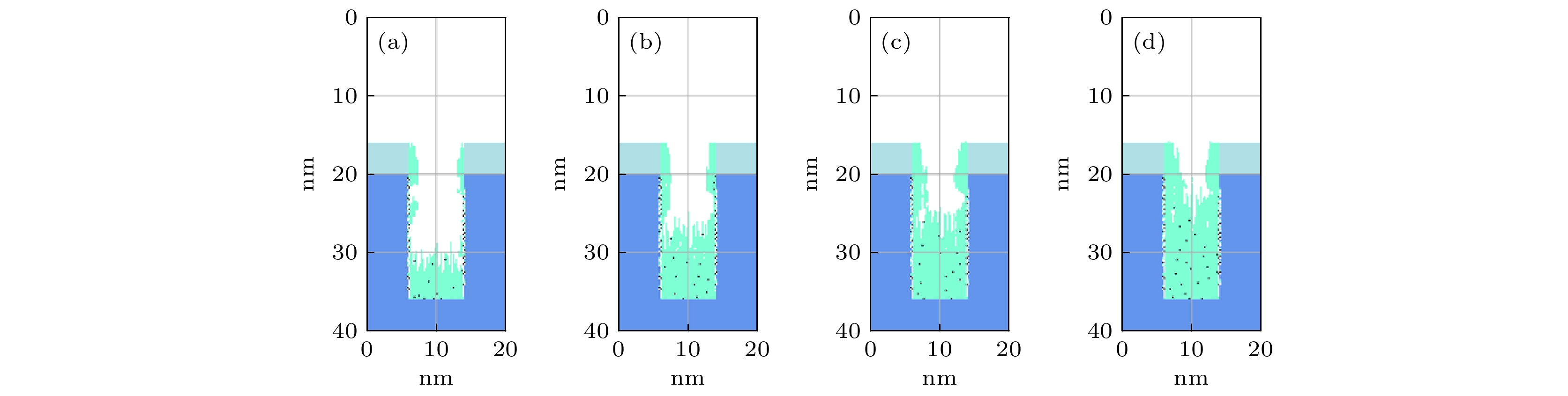
图 13 沉积50 s处于接地极板上不同径向位置处槽结构中的薄膜剖面 (a)
$r=4\;\mathrm{c}\mathrm{m}$ ; (b)$r=10\;\mathrm{c}\mathrm{m}$ ; (c)$r=13\;\mathrm{c}\mathrm{m}$ ; (d)$r= $ $ 14.8\;\mathrm{c}\mathrm{m}$ . 放电气压2 Torr, 气体密度比SiH4/N2O/Ar = 2∶8∶90, 放电频率$f=13.56\text{ MHz}$ , 电压${V}_{\mathrm{s}}=50\text{ V}$ Figure 13. Profiles formed after deposition time(50 s) for different radial positions: (a) r = 4 cm; (b) r = 10 cm; (c) r = 13 cm; (d) r = 14.8 cm. The discharge pressure is 2 Torr, gas density ratio SiH4/N2O/Ar = 2∶8∶90, discharge frequency
$f=13.56\text{ MHz}$ , voltage${V}_{\mathrm{s}}=50\text{ V}$ 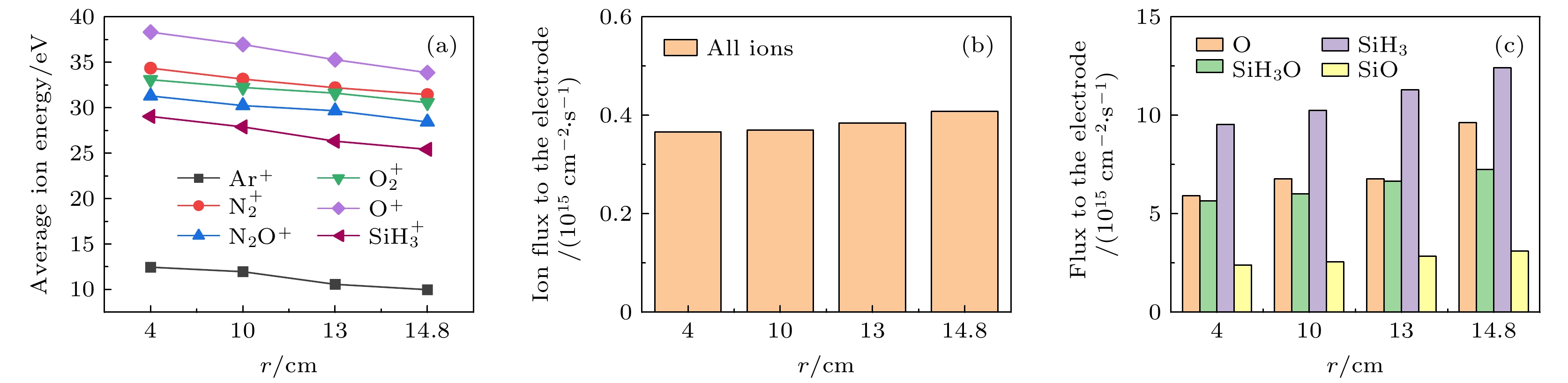
图 14 接地极板上不同径向位置处的(a)各离子平均离子能量和(b)总离子通量(c)中性基团O, SiH3O, SiH3和SiO的通量. 放电气压2 Torr, 气体密度比SiH4/N2O/Ar = 2∶8∶90, 放电频率
$f=13.56\text{ MHz}$ , 电压${V}_{\mathrm{s}}=50\text{ V}$ Figure 14. (a) Average ion energies, (b) fluxes of all ions and (c) fluxes of neutral particles O, SiH3O, SiH3, SiO to the grounded electrode at different radial positions. The discharge pressure is 2 Torr, gas density ratio SiH4/N2O/Ar = 2∶8∶90, discharge frequency
$f=13.56\text{ MHz}$ , voltage${V}_{\mathrm{s}}=50\text{ V}$ 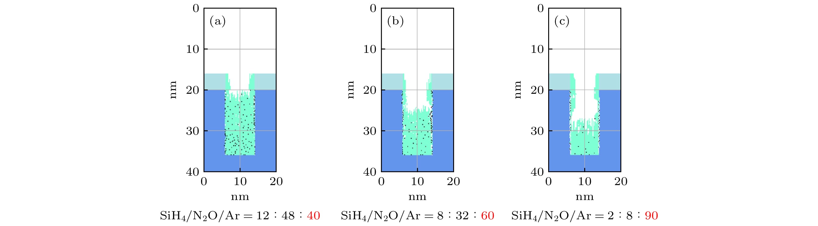
图 15 沉积50 s时, 在接地极板表面
$r=1\;\mathrm{c}\mathrm{m}$ 处的槽结构中薄膜沉积剖面图: SiH4/N2O 密度比固定为2∶ 8, Ar气含量所占比逐渐增大依次为 (a) 40 %; (b) 60 %; (c) 90 %. 放电气压2 Torr, 放电频率$f=13.56\text{ MHz}$ , 电压Vs = 50 VFigure 15. Profiles formed after deposition time of 50 s for different Ar fraction of (a) 40 %, (b) 60 %, and (c) 90 % at the fixed SiH4/N2O density ratio of 2∶8, at the grounded electrode
$r=1\;\mathrm{ }\mathrm{c}\mathrm{m}$ . The discharge pressure is 2 Torr, discharge frequency$f=13.56\text{ MHz}$ , voltage${V}_{\mathrm{s}}=50\text{ V}$ 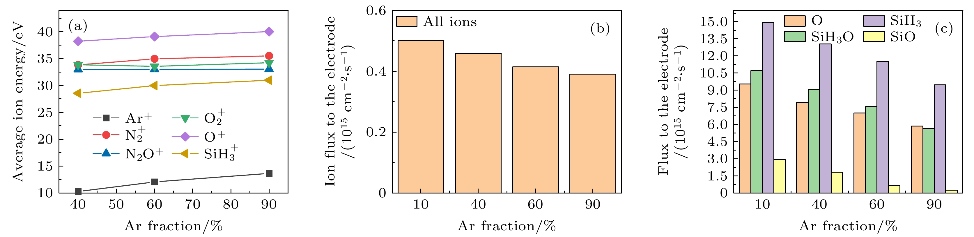
图 16 固定SiH4/N2O密度比为2∶8, 改变Ar含量, 达到接地极板
$r=1\;\mathrm{ }\mathrm{c}\mathrm{m}$ 处 (a) 各离子的平均离子能量; (b) 所有离子通量; (c) 中性基团O, SiH3O, SiH3和SiO的通量. 放电气压2 Torr, 放电频率$f=13.56\text{ MHz}$ , 电压${V}_{\mathrm{s}}=50\text{ V}$ Figure 16. (a) The average energies of ions; (b) the sum flux of all ions; (c) fluxes of neutral particles O, SiH3O, SiH3, SiO to the grounded electrode under different Ar fraction at the fixed SiH4/N2O density ratio of 2∶8. The discharge pressure is 2 Torr, discharge frequency
$f=13.56\text{ MHz}$ , voltage${V}_{\mathrm{s}}=50\text{ V}$ 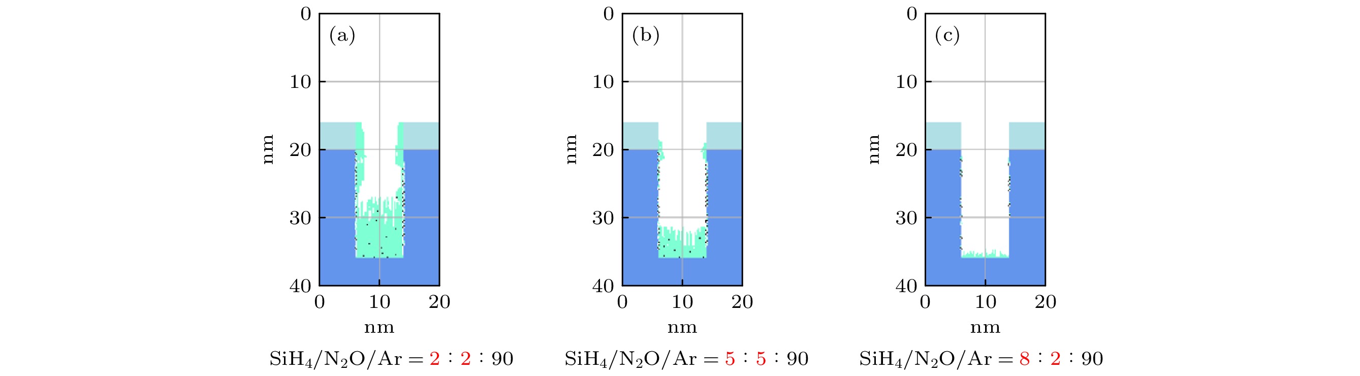
图 17 沉积50 s以后, 在接地极板表面
$r=1\;\mathrm{c}\mathrm{m}$ 处的槽结构中薄膜沉积剖面图 固定氩气含量不变, 增大SiH4/N2O密度比 (a) SiH4/N2O/Ar = 2∶8∶90; (b) SiH4/N2O/Ar = 5∶5∶90; (c) SiH4/N2O/Ar = 8∶2∶90. 放电气压2 Torr, 放电频率$f=13.56\text{ MHz}$ , 电压Vs = 50 VFigure 17. Profiles formed after deposition time (50 s) for different SiH4/N2O density ratios: (a) SiH4/N2O/Ar = 2∶8∶90; (b) SiH4/N2O/Ar = 5∶5∶90; (c) SiH4/N2O/Ar = 8∶2∶90 at the fixed Ar content of 90%, at the grounded electrode
$r=1\;\mathrm{ }\mathrm{c}\mathrm{m}$ . The discharge pressure is 2 Torr, discharge frequency$f=13.56\text{ MHz}$ , voltage${V}_{\mathrm{s}}=50\text{ V}$ 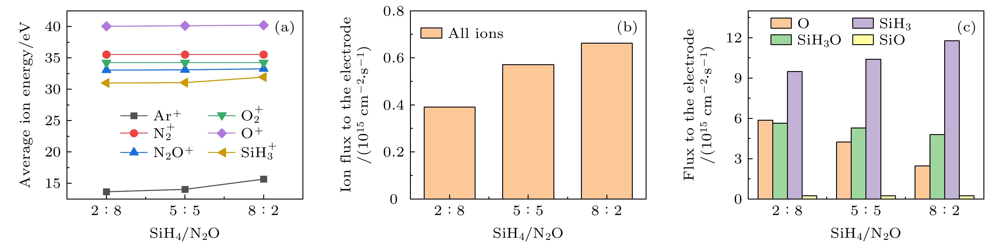
图 18 固定混合气体Ar含量为90%, 改变SiH4/N2O密度比时, 达到接地极板
$r=1\;\mathrm{ }\mathrm{c}\mathrm{m}$ 处 (a) 各离子的平均离子能量; (b) 所有离子通量; (c) 中性基团O, SiH3O, SiH3和SiO的通量. 放电气压2 Torr, 放电频率$f=13.56\text{ MHz}$ , 电压${V}_{\mathrm{s}}=50\text{ V}$ Figure 18. (a) Average energies of ions; (b) the sum flux of all ions; (c) fluxes of neutral particles O, SiH3O, SiH3 and SiO to the grounded electrode under different SiH4/N2O density ratios at the fixed Ar content of 90%. The discharge presuure is 2 Torr, the discharge frequency
$f=13.56\text{ MHz}$ , voltage${V}_{\mathrm{s}}=50\text{ V}$ 表 1 沉积模块考虑的离子溅射反应
Table 1. The ion sputtering reactions considered in the deposition module.
No. Reactions Pi0 εth/eV εref/eV 参考文献 1 Si(s) + Ar+ → Si(g) + Ar 0.20 15 50 [21, 22] 2 SiO(s) + Ar+ → Si(g) + Ar + O 0.20 15 50 [21, 22] 3 SiO2(s) + Ar+ → SiO(g) + Ar + O 0.20 15 50 [21, 22] 4 SiH(s) + Ar+ → SiH(g) + Ar 0.20 15 50 [22] 5 SiH2(s) + Ar+ → SiH2(g) + Ar 0.20 15 50 [22] 6 SiH3(s) + Ar+ → SiH3(g) + Ar 0.20 15 50 [22] 7 SiHO(s) + Ar+ → SiH(g) + Ar + O 0.20 15 50 [22] 8 SiH2O(s) + Ar+ → SiH(g) + Ar + O 0.20 15 50 [22] 9 SiH3O(s) + Ar+ → SiH3(g) + Ar + O 0.20 15 50 [22] 10 SiO2(s) + $\rm SiH_3^+ $ → SiO2(s) + SiH3 0.01614 35 100 [22] 11 Si(s) + H+ → Si(g) + H 0.0007 4/35 100/100 [14, 15] 12 SiO(s) + H+ →Si(g) + OH 0.0007 4/35 100/100 [14, 15] 13 SiO2(s) +H+ →SiO(g) + OH 0.0007 4/35 100/100 [14, 15] 14 SiH(s) + H+ →SiH(g) + H 0.0007 4/35 100/100 [14, 15] 15 SiH2(s) + H+ →SiH2(g) + H 0.0007 4/35 100/100 [14, 15] 16 SiH3(s) + H+ →SiH3(g) + H 0.0007 4/35 100/100 [14, 15] 17 SiHO(s) + H+ →SiH(g) + OH 0.0007 4/35 100/100 [14, 15] 18 SiH2O(s) + H+ →SiH2(g) + OH 0.0007 4/35 100/100 [14, 15] 19 SiH3O(s) + H+ → SiH3(g) + OH 0.007 4/35 100/100 [14, 15] 20 Si(s) + $\rm O_2^+ $ → SiO2(g) 0.20 15 50 [22] 21 SiO(s) + $\rm O_2^+ $ → SiO2(g) + O 0.20 15 50 [22] 22 SiO2(s) + $\rm O_2^+ $ → SiO2(g) + O2 0.0163 35 50 [14, 15] 23 Si(s) + O+ → SiO(g) 0.20 15 50 [22] 24 SiO(s) + O+ → SiO2(g) 0.20 15 50 [22] 25 SiO2(s) + O+ → SiO2(g) + O 0.01153 35 50 [14, 15] 26 SiH4O(s) + O+ → SiO2(g) + 2H2 1.00 35 50 [14, 15] 27 SiO2(s) + N2O+ → SiO2(g) + N2O 0.02 35 100 [15] 28 SiO2(s) + $\rm N_2^+ $ → SiO2(g) + N2 0.02 35 100 [15]  DownLoad: CSV
表 2 沉积模块考虑的中性基团与表面的反应
Table 2. The reactions between neutrals and surfaces considered in the deposition module
No. Reactions Pn0 参考文献 No. Reactions Pn0 参考文献 1 Si(s) + O → SiO(s) 0.99 [22] 26 SiH3O(s) + OH → SiH2O(s) + H2O 1.00 [14, 15] 2 SiO(s) + O → SiO2(s) 0.10 [22] 27 SiH(s) + H → Si (s) + H2 1.00 [22] 3 SiH(s) + O → SiHO(s) 1.00 [22] 28 SiH2(s) + H → SiH (s) + H2 1.00 [22] 4 SiH2(s) + O → SiH2O(s) 1.00 [22] 29 SiH3(s) + H → SiH2(s) + H2 0.955 [22] 5 SiH3(s) + O → SiH3O(s) 1.00 [22] 30 SiH3(s) + H → SiH4(g) 0.045 [22] 6 SiHO(s) + O → SiO(s) + H 1.00 [22] 31 SiHO(s) + H → SiO(s) + H2 1.00 [22] 7 SiH2O(s) + O → SiHO(s) + H 1.00 [22] 32 SiH2O(s) + H → SiHO(s) + H2 1.00 [22] 8 SiH2O(s) + O → SiO2(s) + H2 0.50 [15] 33 SiH3O(s) + H → SiH2O(s) + H2 1.00 [22] 9 SiH3O(s) + O → SiH2O(s) + H2 1.00 [22] 34 SiO(s) + SiH3O → SiO2(s) + SiH3 1.00 [14, 15] 10 SiH4O(s) + O → SiO2(s) + 2H2 1.00 [14, 15] 35 SiHO(s) + SiH3O → SiH3O(s) 1.00 [14, 15] 11 Si(s) + O2 → SiO2(s) 1.00 [22] 36 SiH4O(s) + SiHO → SiO2(s) + SiH3 + H2 1.00 [14, 15] 12 SiO(s) + O2 → SiO2(s) + O 0.99 [22] 37 SiHO(s) + SiHO → SiHO + SiHO(s) 1.00 [22] 13 SiH(s) + O2 → SiHO(s) + O 0.01 [22] 38 Si(s) + SiO → SiO(s) + Si(s) 0.80 [22] 14 SiH2(s) + O2 → SiH2O(s) + O 0.01 [22] 39 SiO(s) + SiO → 2SiO(s) 0.80 [22] 15 SiH3(s) + O2 → SiH3O(s) + O 0.01 [22] 40 SiO2(s) + SiO → SiO(s) + SiO2(s) 0.80 [22] 16 SiHO(s) + O2 → SiO(s) + H + O2 0.01 [22] 41 SiHO(s) + SiO → SiO(s) 1.00 [22] 17 SiH2O(s) + O2 → SiHO(s) + H + O2 0.01 [14] 42 SiH4O(s) + SiO → SiO2(s) + SiH4 1.00 [14, 15] 18 SiH3O(s) + O2 → SiH2O(s) + H + O2 0.01 [22] 43 Si(s) + SiO2 → SiO2(s) + Si(s) 0.80 [22] 19 Si(s) + OH → SiHO(s) 1.00 [22] 44 SiO(s) + SiO2 → SiO2(s) + SiO(s) 0.80 [22] 20 SiO(s) + OH → SiO2(s) + H 1.00 [22] 45 SiO2(s) + SiO2 → SiO2(s) + SiO2(s) 0.80 [22] 21 SiH(s) + OH → SiH2O(s) 1.00 [22] 46 SiO2(s) → SiO2(s) 1.00 [22] 22 SiH2(s) + OH → SiH3O(s) 1.00 [15] 47 SiHO(s) + SiO2 → SiO2(s) 1.00 [22] 23 SiH3(s) + OH → SiH4O(s) 1.00 [15] 48 SiHO(s) + SiH3 → SiH3(s) 0.30 [22] 24 SiHO(s) + OH → SiO(s) + H2O 1.00 [22] 49 SiHO(s) + SiH2O → SiH2O(s) 1.00 [22] 25 SiH2O(s) + OH → SiHO(s) + H2O 1.00 [22]
DownLoad: CSV
-
[1] Nam T, Lee H, Choi T, et al. 2019 Appl. Surf. Sci. 485 381
Google Scholar
[2] Beynet J, Wong P, Miller A, et al. 2009 Proceedings of SPIE - The International Society for Optical Engineering 7520
[3] Lieberman M A, Lichtenberg A J 2005 Principles of Plasma Discharges and Materials Processing (New York: Wiley)
[4] Wuu D, Lo W, Chang L, Horng R 2004 Thin Solid Films 468 105
Google Scholar
[5] Jeong C H, Lee J H, Lim J T, Gil Cho N, Moon C H, Yeom G Y 2005 Jpn. J. Appl. Phys. 44 1022
Google Scholar
[6] Courtney C H, Smith B C, Lamb H H 1998 J. Electrochem. Soc. 145 3957
Google Scholar
[7] Yanguas-Gil A 2017 Growth and Transport in Nanostructured Materials: Reactive Transport in PVD, CVD and ALD (Berlin: Springer)
[8] Alvisi M, De Nunzio G, Di Giulio M, Ferrara M C, Perrone M R, Protopapa L, Vasanelli L 1999 Appl. Opt. 38 1237
Google Scholar
[9] Putkonen M, Bosund M, Ylivaara O M, et al. 2014 Thin Solid Films 558 93
Google Scholar
[10] Özkol E, Procel P, Zhao Y, et al. 2019 Phys. Status Solidi (RRL) Rapid Res. Lett. 14
[11] Pai P, Chao S S, Takagi Y, Lucovsky G 1986 J. Vac. Sci. Technol. A 4 689
Google Scholar
[12] Kushner M J 1993 J. Appl. Phys. 74 6538
Google Scholar
[13] Barron A R 2013 Chemistry of Electronic Materials. (Houston: Rice University) pp1–359
[14] Liu X, Ge J, Yang Y, Song Y, Ren T 2014 Plasma Sci. Technol. 16 385
Google Scholar
[15] Xu Q, Li Y X, Li X N, Wang J B, Yang F, Yang Y 2017 Modern Phys. Lett. B 31 1750055
Google Scholar
[16] Liu R Q, Liu Y, Jia W Z, Zhou Y W 2017 Phys. Plasmas 24 013517
Google Scholar
[17] 贾文柱 2018 博士学位论文 (大连: 大连理工大学)
Jia W Z 2018 Ph. D Dissertation (Dalian: Dalian University of Technology) (in Chinese)
[18] Cheng C C, Guinn K V, Donnelly V M, Herman I P 1994 J. Vac. Sci. Technol. A 12 2630
Google Scholar
[19] Abrams C F, Graves D B 1999 J. Appl. Phys. 86 2263
Google Scholar
[20] Lu Y, Kobayashi A, Kondo, H, Ishikawa K, Sekine M, Hori M 2014 Jpn. J. Appl. Phys. 53 010305
Google Scholar
[21] Tinck S, W Boullart, A Bogaerts 2009 J. Phys. D Appl. Phys. 86 095204
Google Scholar
[22] Qu C, Sakiyama Y, Agarwal P, Kushner M J 2021 J. Vac. Sci. Technol. A 39 052403
Google Scholar
[23] 张赛谦 2018 博士学位论文 (大连: 大连理工大学)
Zhang S Q 2018 Ph. D Dissertation (Dalian: Dalian University of Technology) (in Chinese)
[24] Date L, Radouane K, Despax B, Yousfi M, Caquineau H and Hennad A 1999 J. Phys. D Appl. Phys. 32 1478
Google Scholar

 DownLoad:


Catalog
Metrics
- Abstract views: 3468
- PDF Downloads: 106
- Cited By: 0
