-
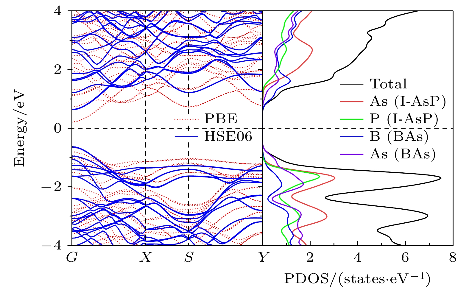
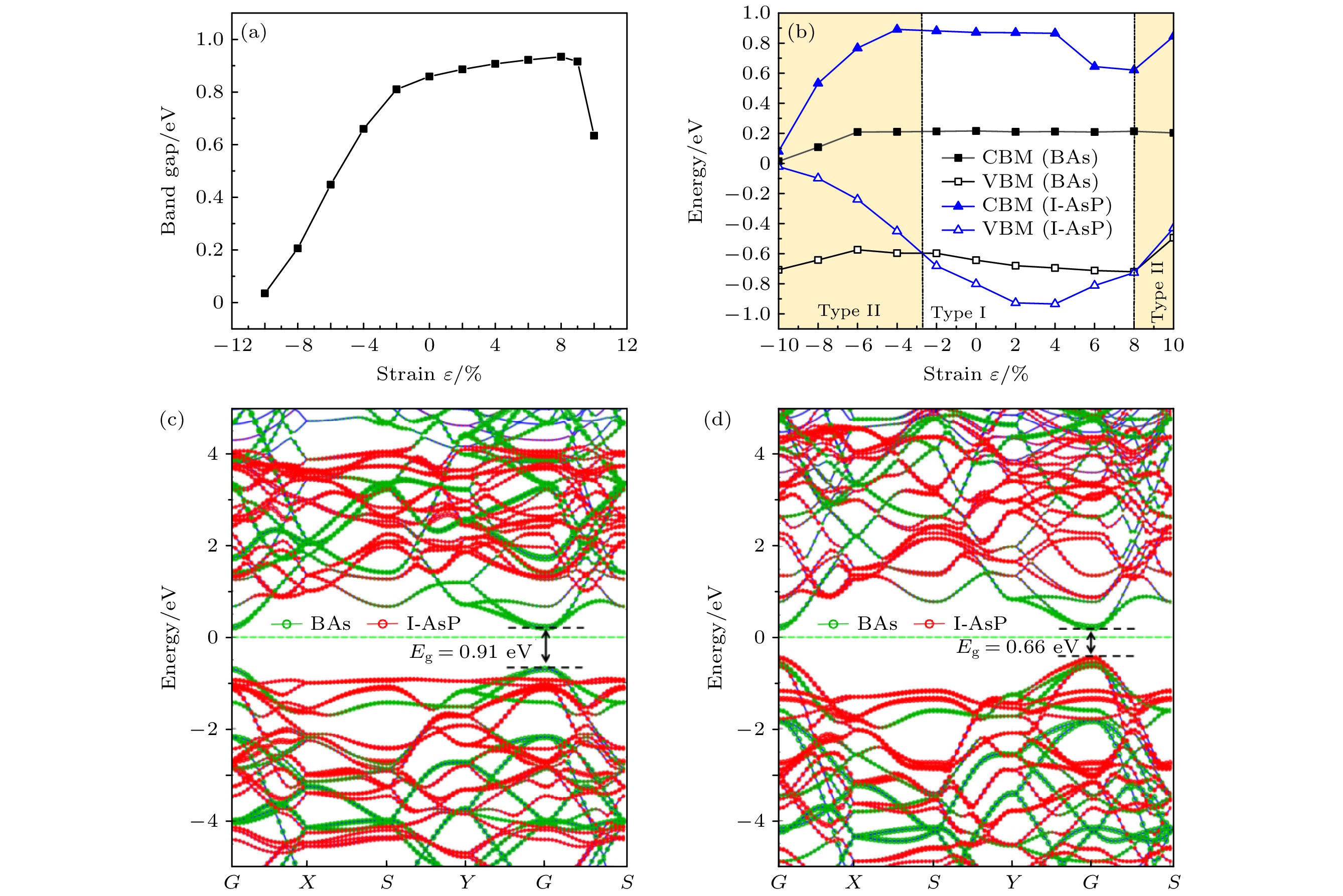
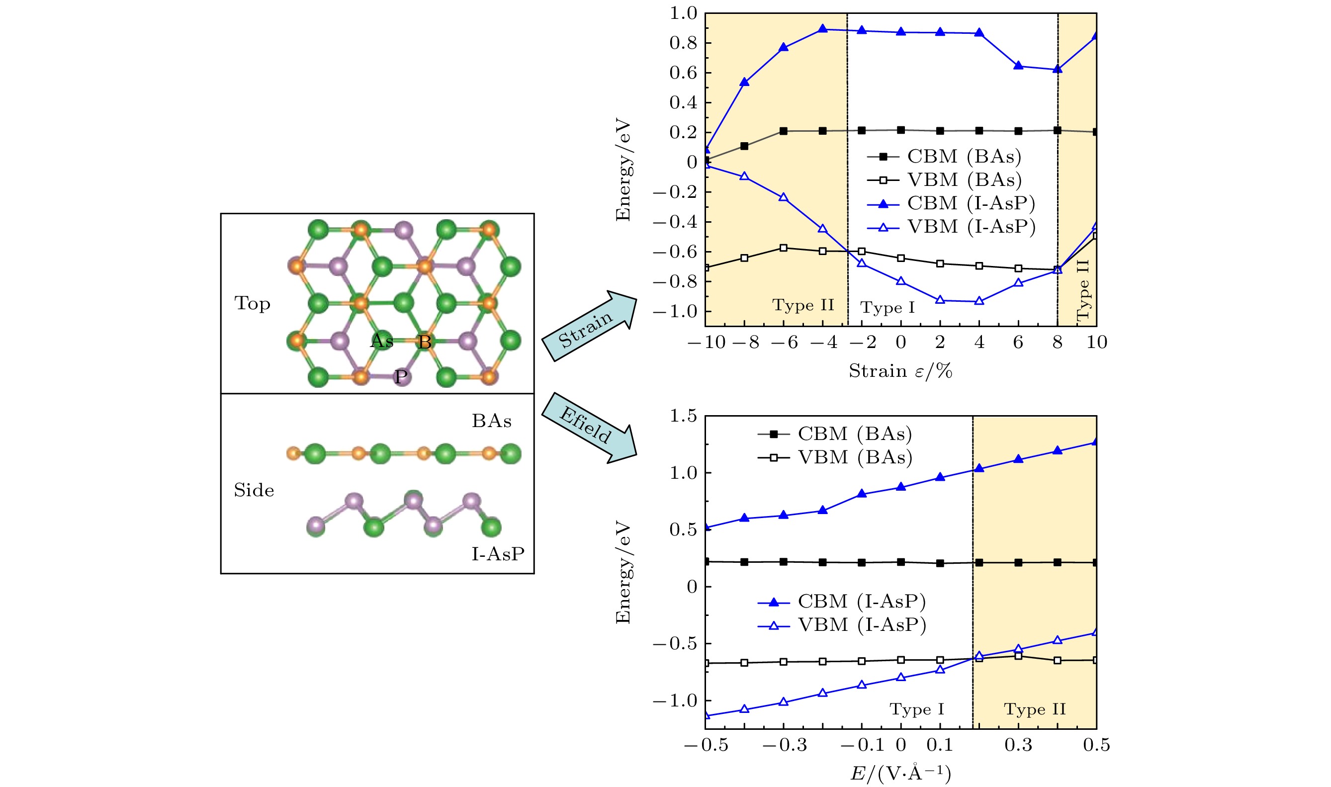
由两种或多种不同的二维材料组合而产生的层状范德瓦耳斯异质结构具有不同寻常的物理特性, 可用于设计高效光电器件. 本文使用基于密度泛函理论的第一性原理方法系统地研究了由二维砷化硼(BAs)和蓝磷砷(I-AsP)单层形成的异质结的几何结构和光电性能. 研究表明, 4种垂直堆叠的BAs/I-AsP异质结构在基态下具有稳定的结构, 且带隙在0.63—0.86 eV之间. 相较于其组分的单层结构, 该异质结构的光学吸收系数得到提升, 并且具备I型能带排列结构. 另外, 通过施加双轴应变和电场可显著地改变异质结构的带隙和能带类型. 在双轴施加–10%—8%的拉伸或压缩应变下, 带隙也随之增大, 在拉伸大于8%时, 带隙开始减小. 电场在–0.5—0.5 V/Å范围内线性地影响带隙, 随着电场增大, 带隙逐渐减小. 双轴应变和电场都可使材料能带排列在I型和II型之间转变. 同时, BAs/I-AsP异质结具有约13%的理论光电转换效率. 可见, 该二维异质结在光伏和光电领域具有广阔的应用前景.In recent years, two-dimensional (2D) materials have attracted considerable attention due to their outstanding optical and electronic properties, and they have shown great potential applications in next-generation solar cells and other optoelectronic devices. In this work, density functional theory (DFT) is used to systematically study the electronic and optoelectronic properties of the heterojunction formed by 2D BAs and I-AsP monolayers, as well as the response of this heterojunction under biaxial strain and electric field. The calculation results show that in the ground state, the four vertically stacked BAs/I-AsP heterostructures all have stable geometric structures, and their band gaps range from 0.63 to 0.86 eV. Compared with their constituent monolayers, these heterostructures have the increased optical absorption coefficients (the absorption coefficient in the x-direction reaches 106 cm–1), and they can effectively separate the photogenerated electron-hole pairs. Of the four structures, the A1 structure exhibits the smallest interlayer spacing, the smallest binding energy, and the highest stability. It has a type-I band alignment and a structure of a direct-band-gap semiconductor with band gaps of 0.86 eV (PBE) and 1.26 eV (HSE06), which can be used in the field of light-emitting diodes. The band gap and band type of the heterostructure can be effectively changed by applying biaxial strain and electric field. Under the application of biaxial tensile or compressive strain in a range of –10% to 8%, the band gap increases accordingly. When the tensile strain is greater than 8%, the band gap starts to decrease. When the biaxial strain ε ≤ –3% and ε > 8%, the heterojunction transitions from a type-I band alignment to a type-II band alignment. Under tensile strain, the absorption spectrum undergoes a red shift, while compressive strain leads to a blue shift of the absorption spectrum. Similarly, the externally applied electric field linearly affects the band gap of the BAs/I-AsP heterojunction in a range from –0.5 to 0.5 V/Å, and the band gap decreases as the electric field increases. When a positive electric field with E ≥ 0.2 V/Å is applied, the band alignment of the heterojunction can also transition from type-I to type-II. The BAs/I-AsP heterojunction has strong absorption properties in the ultraviolet and visible light ranges. Based on the Scharber model, the theoretical power conversion efficiency (PCE) η of the BAs/I-AsP heterojunction is found to be greater than 13%, which is higher than those of 2D heterojunction materials such as Cs3Sb2I9/InSe (η = 3.3%), SiPGaS/As (η = 7.3%) and SnSe/SnS (η = 9.1%). This further expands the application scope of the BAs/I-AsP heterojunction, making it expected to play an important role in the field of photodetectors and solar cells.
[1] Kazem H A, Chaichan M T, Al-Waeli A H A, Sopian K 2024 Sol. Energy 282 112946.
 Google Scholar
[2] Qu W J, Han D J, Zhang J, Peng K W, Gao Y, Huang S M 2025 Energy 316 134562
 Google Scholar
[3] Richter A, Hermle M, Glunz S W 2013 IEEE J. Photovolt. 3 1184
 Google Scholar
[4] An J R, Zhao X Y, Zhang Y N, Liu M X, Yuan J, Sun X J, Zhang Z Y, Wang B, Li S J, Li D B 2022 Adv. Funct. Mater. 32 2110119
 Google Scholar
[5] Zhang J, Zhang H, Du Q, Xie X, Fang Y, Tang C, Chen G 2024 Part. Part. Syst. Charact. 41 2300062
 Google Scholar
[6] Ullah S, Thonhauser T, Menezes M G 2024 Appl. Mater. Today 41 102495
 Google Scholar
[7] Hao J H, Zhang D L, Chen S X, Xu J, Wang Z J, Wang Y F 2025 Surf. Interfaces 58 105837
 Google Scholar
[8] Mao Y L, Wu R L, Ding D, He F 2022 Computat. Mater. Sci. 202 110957
 Google Scholar
[9] Lv B, Lan Y C, Wang X Q, Zhang Q, Hu Y J, Jacobson A J, Broido D, Chen G, Ren Z F, Chu C W 2015 Appl. Phys. Lett. 106 074105
 Google Scholar
[10] Broido D A, Lindsay L, Reinecke T L 2013 Phys. Rev. B 88 214303
 Google Scholar
[11] Xie M Q, Zhang S L, Cai B, Zhu Z, Zou Y S, Zeng H B 2016 Nanoscale 8 13407
 Google Scholar
[12] Xie M Q, Cai B, Meng Z S, Gu Y, Zhang S L, Liu X H, Gong L Y, Li X A, Zeng H B 2020 ACS Appl. Mater. Interfaces 12 6074
 Google Scholar
[13] Mak K F, Shan J 2016 Nat. Photonics 10 216
 Google Scholar
[14] Deng X Q, Sheng R Q, Jing Q 2021 RSC Adv. 11 21824
 Google Scholar
[15] Li L K, Yu Y J, Ye G J, Ge Q Q, Ou X D, Wu H, Feng D L, Chen X H, Zhang Y B 2014 Nat. Nanotechnol. 9 372
 Google Scholar
[16] Zhu Z, Tománek D 2014 Phys. Rev. Lett. 112 176802
 Google Scholar
[17] Song Y H, Muzaffar M U, Wang Q, Wang Y, Jia Y, Cui P, Zhang W, Wang X S, Zhang Z 2024 Nat. Commun. 15 1157
 Google Scholar
[18] Zhou D C, Meng Q L, Si N, Zhou X, Zhai S W, Tang Q, Ji Q M, Zhou M, Niu T C, Fuchs H 2020 ACS Nano 14 2385
 Google Scholar
[19] Cheng W J, Yao X D, Zhao L X, Li C K, Zheng Q F, Han J, Wang S M, Liu Y, Zhu J L 2024 Phys. Rev. B 109 064507
 Google Scholar
[20] Antonatos N, Mazánek V, Lazar P, Sturala J, Sofer Z 2020 Nanoscale Adv. 2 1282
 Google Scholar
[21] Jamdagni P, Thakur A, Kumar A, Ahluwalia P K, Pandey R 2018 Phys. Chem. Chem. Phys. 20 29939
 Google Scholar
[22] Zhang S L, Yan Z, Li Y F, Chen Z F, Zeng H B 2015 Angew. Chem. Int. Edt. 54 3112
 Google Scholar
[23] Zhong M Z, He J 2020 J. Semicond. 41 080402
 Google Scholar
[24] Yuan S F, Shen C F, Deng B C, Chen X L, Guo Q S, Ma Y Q, Abbas A, Liu B L, Haiges R, Ott C, Nilges T, Watanabe K, Taniguchi T, Sinai O, Naveh D, Zhou C W, Xia F N 2018 Nano Lett. 18 3172
 Google Scholar
[25] Cai X Y, Chen Y Z, Sun B, Chen J, Wang H Y, Ni Y X, Tao L, Wang H, Zhu S H, Li X M, Wang Y C, Lv J, Feng X L, Redfern S A T, Chen Z F 2019 Nanoscale 11 8260
 Google Scholar
[26] Blöchl P E 1994 Phys. Rev. B 50 17953
 Google Scholar
[27] Kresse G, Joubert D 1999 Phys. Rev. B 59 1758
 Google Scholar
[28] Perdew J P, Burke K, Ernzerhof M 1996 Phys. Rev. Lett. 77 3865
 Google Scholar
[29] Grimme S, Antony J, Ehrlich S, Krieg H 2010 J. Chem. Phys. 132 154104
 Google Scholar
[30] Hao J H, Zhang D L, Wang Z J, Chen S X, Xu J, Wang Y F 2024 Mater. Today Commun. 38 108423
 Google Scholar
[31] Monkhorst H J, Pack J D 1976 Phys. Rev. B 13 5188
 Google Scholar
[32] Nosé S 1984 J. Chem. Phys. 81 511
 Google Scholar
[33] Tang W, Sanville E, Henkelman G 2009 J. Phys. Condens. Mater. 21 084204
 Google Scholar
[34] Bai H, Qian G L, Liang Q, Feng Y Y, An M Y, Xie Q 2024 Comput. Mater. Sci. 238 112948
 Google Scholar
[35] Cheng K, Xu J K, Guo X, Guo S D, Su Y 2023 Phys. Chem. Chem. Phys. 25 17360
 Google Scholar
[36] Wu H Y, Yang K, Si Y, Huang W Q, Hu W, Huang G F 2019 Phys. Status Solidi RRL 13 1800565
 Google Scholar
[37] 孙婷钰, 吴量, 何贤娟, 姜楠, 周文哲, 欧阳方平 2023 物理学报 72 076301
 Google Scholar
Sun T Y, Wu L, He X J, Jiang N, Zhou W Z, Ouyang F P 2023 Acta Phys. Sin. 72 076301
 Google Scholar
[38] Bernardi M, Palummo M, Grossman J C 2012 ACS Nano 6 10082
 Google Scholar
[39] Wu M, Meng D 2024 Physics B 680 415847
 Google Scholar
[40] Behzad S, Chegel R 2023 Sci. Rep. 13 21339
 Google Scholar
[41] Lin L, Lou M S, Li S F, Cai X L, Zhang Z W, Tao H L 2022 Appl. Surf. Sci. 572 151209
 Google Scholar
[42] 刘晨曦, 庞国旺, 潘多桥, 史蕾倩, 张丽丽, 雷博程, 赵旭才, 黄以能 2022 物理学报 71 097301
 Google Scholar
Liu C X, Pang G W, Pan D Q, Shi L Q, Zhang L L, Lei B C, Zhao X C, Huang Y N 2022 Acta Phys. Sin. 71 097301
 Google Scholar
[43] Xu Y H, Fan Z Q, Zhang Z H, Zhao T 2021 Appl. Surf. Sci. 547 149174
 Google Scholar
[44] 熊祥杰, 钟防, 张资文, 陈芳, 罗婧澜, 赵宇清, 朱慧平, 蒋绍龙 2024 物理学报 73 137101
 Google Scholar
Xiong X J, Zhong F, Zhang Z W, Chen F, Luo J L, Zhao Y Q, Zhu H P, Jiang S L 2024 Acta Phys. Sin. 73 137101
 Google Scholar
[45] Shahid I, Hu X, Ahmad I, Ali A, Shehzad N, Ahmad S, Zhou Z 2023 Nanoscale 15 7302
 Google Scholar
[46] Zhang R Q, Zhou Z Z, Yao Q, Qi N, Chen Z Q 2021 Phys. Chem. Chem. Phys. 23 3794
 Google Scholar
-
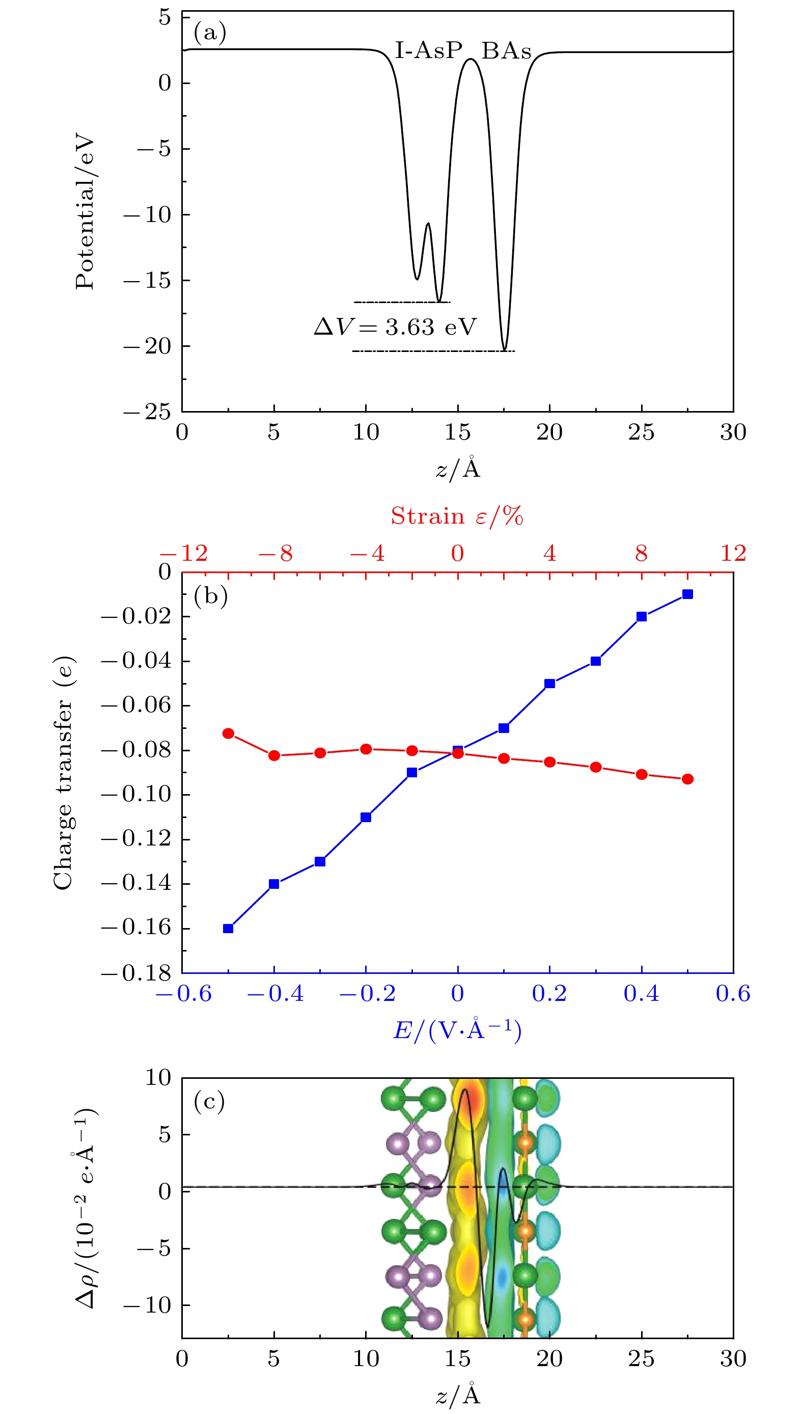
图 5 (a) BAs/I-AsP异质结界面电位分布; (b)异质结的Bader电荷分析结果(负值代表电荷由BAs层转移至I-AsP层); (c) BAs/I-AsP异质结构沿z方向的平面平均电荷密度差Δρ(z), 其中插图展示了电荷密度差的三维等值面(黄色和蓝色区域分别表示电子增加和减少)
Fig. 5. (a) The interfacial potential distribution of the BAs/I-AsP heterojunction; (b) results of the Bader charge analysis of the heterojunction, the negative values indicate that the charge is transferred from the BAs layer to the I-AsP layer; (c) the planar average charge density difference Δρ(z) of the BAs/I-AsP heterostructure along the z direction of the surface. The inset shows the three-dimensional isosurface of the charge density difference (the yellow and blue regions represent the increase and decrease of electrons respectively).
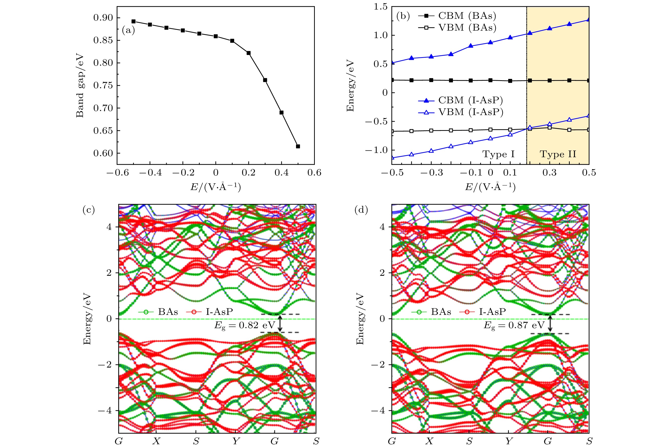
图 7 BAs/I-AsP异质结构在外加电场下的变化 (a)带隙变化; (b)能带边缘变化; (c), (d) E = 0.2 V/Å和–0.2 V/Å的能带结构
Fig. 7. Variation of the BAs/I-AsP heterostructure under an externally applied electric field: (a) Variation of the band gap; (b) variation of the band edges; (c) the energy band structure with E = 0.2 V/Å and –0.2 V/Å, respectively.
图 8 (a)单层BAs、单层I-AsP与BAs/I-AsP异质结沿x轴和z轴的光吸收系数; (b) BAs/I-AsP异质结在不同双轴应变下沿x轴和z轴的光吸收系数变化情况; (c) BAs/I-AsP异质结在不同外加电场作用下沿x轴和z轴的光吸收系数变化情况
Fig. 8. (a) The optical absorption coefficients along the x-axis and z-axis of the monolayer BAs, I-AsP and the BAs/I-AsP heterojunction; (b) variations of the optical absorption coefficients along the x-axis and z-axis of the BAs/I-AsP heterojunction under different biaxial strains; (c) variations of the optical absorption coefficients along the x-axis and z-axis of the BAs/I-AsP heterojunction under different applied electric fields.
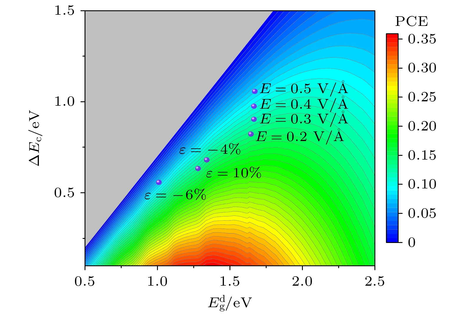
图 9 BAs/I-AsP异质结的光电转换效率随导带偏移量$ \Delta {E}_{{\mathrm{c}}} $和施主带隙$ {E}_{{\mathrm{g}}}^{{\mathrm{d}}} $变化的等高线图
Fig. 9. Contour plot of the photoelectric conversion efficiency of the BAs/I-AsP heterojunction as a function of the conduction band offset ($ \Delta {E}_{{\mathrm{c}}} $) and the donor band gap ($ {E}_{{\mathrm{g}}}^{{\mathrm{d}}} $).
表 1 单层BAs、单层I-AsP以及4种堆叠构型的结构参数, 包括晶格常数(其中a = b)、层间距(d)、键长(l)、带隙(Eg)和层间结合能(Eb)
Table 1. Structural parameters for monolayer BAs, monolayer I-AsP, and four stacking configurations in heterostructures, include lattice constants (where a = b), interlayer distance (d), bond length (l), band gap (Eg), and interlayer binding energy (Eb).
a/Å d/Å lB-As/Å(lAs-As/lAs-P/lP-P) Eg/eV Eb/(meV·Å–2) PBE HSE06 BAs 3.39 — 1.96 0.76 1.18 — I-AsP 5.87 — 2.49/2.37/2.24 1.63 2.27 — A1 5.87 3.44 1.96 (2.49/2.37/2.24) 0.86 1.26 –0.59 A2 5.87 3.83 1.96 (2.49/2.37/2.24) 0.63 — –0.43 A3 5.87 3.60 1.96 (2.49/2.37/2.24) 0.79 — –0.52 A4 5.87 3.81 1.96 (2.49/2.37/2.24) 0.71 — –0.47 表 2 施加双轴应变和外加电场下具有II型能带排列的异质结构的光伏特性相关参数
Table 2. Summary of the photovoltaic characteristic parameters of the heterostructures with type-II band alignment under the biaxial strain and the external electric field.
Strain/% $ {E}_{{\mathrm{g}}}^{{\mathrm{d}}} $/eV $ \Delta {E}_{{\mathrm{c}}} $/eV $ {V}_{{\mathrm{o}}{\mathrm{c}}} $/V $ \eta $/% –4 1.34 0.681 0.359 13.14 –6 1.01 0.558 0.152 7.49 10 1.28 0.634 0.334 12.72 Electric field/(V·Å–1) $ {E}_{{\mathrm{g}}}^{{\mathrm{d}}} $/eV $ \Delta {E}_{{\mathrm{c}}} $/eV $ {V}_{{\mathrm{o}}{\mathrm{c}}} $/V $ \eta $/% 0.2 1.64 0.823 0.522 13.13 0.3 1.66 0.904 0.462 11.26 0.4 1.67 0.976 0.390 9.51 0.5 1.67 1.057 0.315 8.09 -
[1] Kazem H A, Chaichan M T, Al-Waeli A H A, Sopian K 2024 Sol. Energy 282 112946.
 Google Scholar
[2] Qu W J, Han D J, Zhang J, Peng K W, Gao Y, Huang S M 2025 Energy 316 134562
 Google Scholar
[3] Richter A, Hermle M, Glunz S W 2013 IEEE J. Photovolt. 3 1184
 Google Scholar
[4] An J R, Zhao X Y, Zhang Y N, Liu M X, Yuan J, Sun X J, Zhang Z Y, Wang B, Li S J, Li D B 2022 Adv. Funct. Mater. 32 2110119
 Google Scholar
[5] Zhang J, Zhang H, Du Q, Xie X, Fang Y, Tang C, Chen G 2024 Part. Part. Syst. Charact. 41 2300062
 Google Scholar
[6] Ullah S, Thonhauser T, Menezes M G 2024 Appl. Mater. Today 41 102495
 Google Scholar
[7] Hao J H, Zhang D L, Chen S X, Xu J, Wang Z J, Wang Y F 2025 Surf. Interfaces 58 105837
 Google Scholar
[8] Mao Y L, Wu R L, Ding D, He F 2022 Computat. Mater. Sci. 202 110957
 Google Scholar
[9] Lv B, Lan Y C, Wang X Q, Zhang Q, Hu Y J, Jacobson A J, Broido D, Chen G, Ren Z F, Chu C W 2015 Appl. Phys. Lett. 106 074105
 Google Scholar
[10] Broido D A, Lindsay L, Reinecke T L 2013 Phys. Rev. B 88 214303
 Google Scholar
[11] Xie M Q, Zhang S L, Cai B, Zhu Z, Zou Y S, Zeng H B 2016 Nanoscale 8 13407
 Google Scholar
[12] Xie M Q, Cai B, Meng Z S, Gu Y, Zhang S L, Liu X H, Gong L Y, Li X A, Zeng H B 2020 ACS Appl. Mater. Interfaces 12 6074
 Google Scholar
[13] Mak K F, Shan J 2016 Nat. Photonics 10 216
 Google Scholar
[14] Deng X Q, Sheng R Q, Jing Q 2021 RSC Adv. 11 21824
 Google Scholar
[15] Li L K, Yu Y J, Ye G J, Ge Q Q, Ou X D, Wu H, Feng D L, Chen X H, Zhang Y B 2014 Nat. Nanotechnol. 9 372
 Google Scholar
[16] Zhu Z, Tománek D 2014 Phys. Rev. Lett. 112 176802
 Google Scholar
[17] Song Y H, Muzaffar M U, Wang Q, Wang Y, Jia Y, Cui P, Zhang W, Wang X S, Zhang Z 2024 Nat. Commun. 15 1157
 Google Scholar
[18] Zhou D C, Meng Q L, Si N, Zhou X, Zhai S W, Tang Q, Ji Q M, Zhou M, Niu T C, Fuchs H 2020 ACS Nano 14 2385
 Google Scholar
[19] Cheng W J, Yao X D, Zhao L X, Li C K, Zheng Q F, Han J, Wang S M, Liu Y, Zhu J L 2024 Phys. Rev. B 109 064507
 Google Scholar
[20] Antonatos N, Mazánek V, Lazar P, Sturala J, Sofer Z 2020 Nanoscale Adv. 2 1282
 Google Scholar
[21] Jamdagni P, Thakur A, Kumar A, Ahluwalia P K, Pandey R 2018 Phys. Chem. Chem. Phys. 20 29939
 Google Scholar
[22] Zhang S L, Yan Z, Li Y F, Chen Z F, Zeng H B 2015 Angew. Chem. Int. Edt. 54 3112
 Google Scholar
[23] Zhong M Z, He J 2020 J. Semicond. 41 080402
 Google Scholar
[24] Yuan S F, Shen C F, Deng B C, Chen X L, Guo Q S, Ma Y Q, Abbas A, Liu B L, Haiges R, Ott C, Nilges T, Watanabe K, Taniguchi T, Sinai O, Naveh D, Zhou C W, Xia F N 2018 Nano Lett. 18 3172
 Google Scholar
[25] Cai X Y, Chen Y Z, Sun B, Chen J, Wang H Y, Ni Y X, Tao L, Wang H, Zhu S H, Li X M, Wang Y C, Lv J, Feng X L, Redfern S A T, Chen Z F 2019 Nanoscale 11 8260
 Google Scholar
[26] Blöchl P E 1994 Phys. Rev. B 50 17953
 Google Scholar
[27] Kresse G, Joubert D 1999 Phys. Rev. B 59 1758
 Google Scholar
[28] Perdew J P, Burke K, Ernzerhof M 1996 Phys. Rev. Lett. 77 3865
 Google Scholar
[29] Grimme S, Antony J, Ehrlich S, Krieg H 2010 J. Chem. Phys. 132 154104
 Google Scholar
[30] Hao J H, Zhang D L, Wang Z J, Chen S X, Xu J, Wang Y F 2024 Mater. Today Commun. 38 108423
 Google Scholar
[31] Monkhorst H J, Pack J D 1976 Phys. Rev. B 13 5188
 Google Scholar
[32] Nosé S 1984 J. Chem. Phys. 81 511
 Google Scholar
[33] Tang W, Sanville E, Henkelman G 2009 J. Phys. Condens. Mater. 21 084204
 Google Scholar
[34] Bai H, Qian G L, Liang Q, Feng Y Y, An M Y, Xie Q 2024 Comput. Mater. Sci. 238 112948
 Google Scholar
[35] Cheng K, Xu J K, Guo X, Guo S D, Su Y 2023 Phys. Chem. Chem. Phys. 25 17360
 Google Scholar
[36] Wu H Y, Yang K, Si Y, Huang W Q, Hu W, Huang G F 2019 Phys. Status Solidi RRL 13 1800565
 Google Scholar
[37] 孙婷钰, 吴量, 何贤娟, 姜楠, 周文哲, 欧阳方平 2023 物理学报 72 076301
 Google Scholar
Sun T Y, Wu L, He X J, Jiang N, Zhou W Z, Ouyang F P 2023 Acta Phys. Sin. 72 076301
 Google Scholar
[38] Bernardi M, Palummo M, Grossman J C 2012 ACS Nano 6 10082
 Google Scholar
[39] Wu M, Meng D 2024 Physics B 680 415847
 Google Scholar
[40] Behzad S, Chegel R 2023 Sci. Rep. 13 21339
 Google Scholar
[41] Lin L, Lou M S, Li S F, Cai X L, Zhang Z W, Tao H L 2022 Appl. Surf. Sci. 572 151209
 Google Scholar
[42] 刘晨曦, 庞国旺, 潘多桥, 史蕾倩, 张丽丽, 雷博程, 赵旭才, 黄以能 2022 物理学报 71 097301
 Google Scholar
Liu C X, Pang G W, Pan D Q, Shi L Q, Zhang L L, Lei B C, Zhao X C, Huang Y N 2022 Acta Phys. Sin. 71 097301
 Google Scholar
[43] Xu Y H, Fan Z Q, Zhang Z H, Zhao T 2021 Appl. Surf. Sci. 547 149174
 Google Scholar
[44] 熊祥杰, 钟防, 张资文, 陈芳, 罗婧澜, 赵宇清, 朱慧平, 蒋绍龙 2024 物理学报 73 137101
 Google Scholar
Xiong X J, Zhong F, Zhang Z W, Chen F, Luo J L, Zhao Y Q, Zhu H P, Jiang S L 2024 Acta Phys. Sin. 73 137101
 Google Scholar
[45] Shahid I, Hu X, Ahmad I, Ali A, Shehzad N, Ahmad S, Zhou Z 2023 Nanoscale 15 7302
 Google Scholar
[46] Zhang R Q, Zhou Z Z, Yao Q, Qi N, Chen Z Q 2021 Phys. Chem. Chem. Phys. 23 3794
 Google Scholar
计量
- 文章访问数: 2328
- PDF下载量: 76
- 被引次数: 0



 下载:
下载:


