


-
采用简单的水热法结合热处理工艺, 制备了高纯、形貌可控的纳米VO2 (M)颗粒, 得到了退火时间对颗粒形貌的影响, 首次揭示了VO2聚乙二醇复合薄膜电致相变过程, 建立了电致相变模型. 实验以V2O5和H2C2O4·2H2O为原料, 经180 ℃, 12 h水热处理后, 得到VO2 (B)纳米颗粒, 真空退火转化为VO2 (M). 结果表明, 退火时间越长, 纳米颗粒长度越短. 多次重复测试发现, 复合薄膜在电场作用下, 均能够发生显著的相变现象, 但同一样品的重复相变电压低于第1次测试数据. 在首次测试后, 相变电压和非线性系数随纳米VO2的长度减小而指数增加, 同时发现材料两端电压在相变后可维持在10 V附近. 分析认为, 复合薄膜的相变电压和非线性系数由颗粒内势垒和界面间势垒共同决定. 首次伏安测试降低了颗粒间势垒, 造成了材料的“激活”现象, 纳米颗粒平均长度越短, 导电通道中的界面间势垒越多, 导致相变电压和非线性系数升高. 实验发现, 电场作用是复合薄膜相变发生的决定因素, 相变后焦耳热对维持相变起主要作用.In this paper, the voltage induced metal-insulator phase transition (MIT) of polyethene glycol (PEG) composite film is investigated based on VO2 nanoparticles prepared by the hydrothermal method and vacuum annealing process. High purity VO2 (B) nanoparticles are obtained after being treated in a hydrothermal reactor at 180 ℃ for 12 h by using vanadium pentoxide (V2O5) and oxalic acid (H2C2O4·2H2O) as raw materials. The X-ray diffraction (XRD) pattern shows that the prepared nano-powders are free of impurities, and the scanning electron microscope (SEM) pictures confirm that the micro-morphology is of a band-shaped nano-structure. Next, these products are heated in a vacuum quartz tube at 500 ℃ for different times. The XRD and differential scanning calorimeter (DSC) curves of the annealed samples prove that the VO2 (M) with MIT performance is successfully prepared. And the content of M phase in the sample increases with preparation time increasing. When the annealing time is longer than 60 min, all the samples are converted into materials with M phase. The SEM images show that the average length of the nano-powders decreases with the annealing time increasing from 10 min to 300 min. Then PEG coating containing VO2 (M) nanoparticles is applied between two electrodes with a pitch of 1 mm on printed circuit board (PCB). The V-I test is carried out after a 20 kΩ resistor has been connected in the circuit. The results display repeatable non-linear V-I curves indicating that the composite film undergoes an MIT phase transition under voltage. After it is activated for the first test, the MIT voltage and non-linear coefficient increase exponentially as the length of VO2 decreases. Besides, it is also found that the voltage across the material is maintained at around 10 V after the resistance has changed suddenly, which is similar to the behavior of diode clamping voltage. We believe that the phase transition voltage and non-linear coefficient of the VO2 composite film are influenced by the intra-particle potential barrier and the inter-layer potential barrier. The longer the average length of the nanoparticles, the higher the potential barrier between the interfaces in the conductive channels is, and thus increasing the phase transition voltage and phase transition coefficient. The activation phenomenon of the thin film is caused by reducing the barrier between particles during the first test. Furthermore, the results can prove that the electric field is the determinant of the phase transition during the VO2 composite film electrical field induced MIT of the VO2 composite film. However, after the phase transition, Joule heat plays a significant role in maintaining the low resistance state.
-
Keywords:
- vanadium dioxide /
- vacuum annealing /
- electrical field induced phase transition /
- potential barrier
[1] Surnev S, Ramsey M G, Netzer F P 2003 Prog. Surf. Sci. 73 117
 Google Scholar
[2] Stefanovich G, Pergament A, Stefanovich D 2000 J. Phys. Condens. Matter 12 8837
Google Scholar
[3] Karakotsou C, Anagnostopoulos A N, Kambas K, Spyridelis J 1992 Phys. Rev. B 46 16144
Google Scholar
[4] Morin F J 1959 Phys. Rev. Lett. 3 34
Google Scholar
[5] 王庆国, 何长安, 曲兆明, 山世浩, 李昂, 成伟, 王妍 2018 安全与电磁兼容 2018 14
Wang Q G, He C A, Qu Z M, Shan S H, Li A, Cheng W, Wang Y 2018 Safety & EMC 2018 14
[6] Yang Z, Ko C, Ramanathan S 2011 Annu. Rev. Mater. Res. 41 337
Google Scholar
[7] Becker M F, Buckman A B, Walser R M, Lépine T, Georges P, Brun A 1996 J. Appl. Phys. 79 2404
Google Scholar
[8] Ji S, Zhao Y, Zhang F, Jin P 2010 J. Cryst. Growth 312 282
Google Scholar
[9] Zhang Y, Zhang J, Zhang X, Mo S, Wu W, Niu F, Zhong Y, Liu X, Huang C, Liu X 2013 J. Alloys Compd. 570 104
Google Scholar
[10] Zhang K F, Bao S J, Liu X, Shi J, Su Z X, Li H L 2006 Mater. Res. Bull. 41 1985
Google Scholar
[11] Song Z D, Zhang L M, Xia F, Webster N A, Song J, Liu B, Luo H, Gao Y 2016 Inorg. Chem. Front. 3 1035
Google Scholar
[12] Ji S, Zhang F, Jin P 2011 J. Solid State Chem. 184 2285
Google Scholar
[13] 张娇, 李毅, 刘志敏, 李政鹏, 黄雅琴, 裴江恒, 方宝英, 王晓华, 肖寒 2017 物理学报 66 238101
Google Scholar
Zhang J, Li Y, Liu Z M, Li Z P, Huang Y Q, Pei J H, Fang B Y, Wang X H, Xiao H 2017 Acta Phys. Sin. 66 238101
Google Scholar
[14] 覃源, 李毅, 方宝英, 佟国香, 王晓华, 丁杰, 王峰, 严梦, 梁倩, 陈少娟 2013 光学学报 33 343
Google Scholar
Qin Y, Li Y, Fang B Y, Tong G X, Wang X H, Ding J, Wang F, Yan M, Liang Q, Chen S J 2013 Acta Opt. Sin. 33 343
Google Scholar
[15] Chen L, Wang X, Wan D, Cui Y, Liu B, Shi S, Luo H, Gao Y 2016 RSC Adv. 6 73070
Google Scholar
[16] Ji S, Zhang F, Jin P 2011 Sol. Energy Mater. Sol. Cells 95 3520
Google Scholar
[17] Rathi S, Lee I y, Park J H, Kim B J, Kim H T, Kim G H 2014 ACS Appl. Mater. Interfaces 6 19718
Google Scholar
[18] Kozo T, Li Z C, Wang Y Q, Ni J, Hu Y, Zhang Z J 2009 Front. Mater. Sci. Chin. 3 48
Google Scholar
[19] Kumar M, Singh J P, Chae K H, Park J, Lee H H 2020 Superlattices Microstruct. 137 106335
Google Scholar
[20] Meng Y F, Sang J X, Liu Z, Xu X F, Tan Z Y, Wang C R, Wu B H, Wang C, Cao J C, Chen X S 2019 Appl. Surf. Sci. 470 168
Google Scholar
[21] Rathi S, Park J H, Lee I, Jin Kim M, Min Baik J, Kim G H 2013 Appl. Phys. Lett. 103 203114
Google Scholar
[22] Xu H Y, Huang Y H, Liu S, Xu K W, Ma F, Chu P K 2016 RSC Adv. 137 79383
Google Scholar
[23] Afify H H, Hassan S A, Obaida M, Abouelsayed A 2019 Physica E 114 113610
Google Scholar
[24] 罗明海, 徐马记, 黄其伟, 李派, 何云斌 2016 物理学报 65 047201
Google Scholar
Luo M H, Xu M J, Huang Q W, Li P, He Y B 2016 Acta Phys. Sin. 65 047201
Google Scholar
[25] Dai L, Cao C, Gao Y, Luo H 2011 Sol. Energy Mater. Sol. Cells 95 712
Google Scholar
[26] Wu C, Zhang X, Dai J, Yang J, Wu Z, Wei S, Xie Y 2011 J. Mater. Chem. 21 4509
Google Scholar
[27] Antonova K V, Kolbunov V R, Tonkoshkur A S 2014 J. Polym. Res. 21 422
Google Scholar
[28] Pillai S C, Kelly J M, Ramesh R, McCormack D E 2013 J. Mater. Chem. C 1 3268
Google Scholar
[29] Qazilbash M M, Brehm M, Chae B G, Ho P C, Andreev G O, Kim B J, Yun S J, Balatsky A V, Maple M B, Keilmann F, Kim H T, Basov D N 2007 Science 318 1750
Google Scholar
[30] Zylbersztejn A, Mott N F 1975 Phys. Rev. B 11 4383
Google Scholar
[31] Gervais F, Kress W 1985 Phys. Rev. B 31 4809
Google Scholar
[32] 孙肖宁, 曲兆明, 王庆国, 袁扬, 刘尚合 2019 物理学报 68 107201
Google Scholar
Sun X N, Qu Z M, Wang Q G, Yuan Y, Liu S H 2019 Acta Phys. Sin. 68 107201
Google Scholar
[33] Rozen J, Lopez R, Haglund R F, Feldman L C 2006 Appl. Phys. Lett. 88 081902
Google Scholar
[34] He X F, Xu J, Xu X F, Gu C C, Chen F, Wu B H, Wang C R, Xing H Z, Chen X S, Chu J H 2015 Appl. Phys. Lett. 106 093106
Google Scholar
[35] Kumar S, Pickett M D, Strachan J P, Gibson G, Nishi Y, Williams R S 2013 Adv. Mater. 25 6128
Google Scholar
[36] Singh S, Horrocks G, Marley P M, Shi Z, Banerjee S, Sambandamurthy G 2015 Phys. Rev. B 92 155121
Google Scholar
[37] Joushaghani A, Jeong J, Paradis S, Alain D, Stewart Aitchison J, Poon J K S 2014 Appl. Phys. Lett. 105 231904
Google Scholar
[38] Zeng W, Chen N, Xie W G 2020 Cryst. Eng. Comm. 22 851
Google Scholar
[39] Whittaker L, Jaye C, Fu Z, Fischer D A, Banerjee S 2009 J. Am. Chem. Soc. 131 8884
Google Scholar
[40] Wang Z S, Zeng F, Yang J, Chen C, Pan F 2012 ACS Appl. Mater. Interfaces 4 447
Google Scholar
[41] Mamunya E P, Davidenko V V, Lebedev E V 1996 Compos. Interfaces 4 169
Google Scholar
[42] Yang W, Wang J, Luo S, Yu S, Huang H, Sun R, Wong C P 2016 ACS Appl. Mater. Interfaces 8 35545
Google Scholar
-
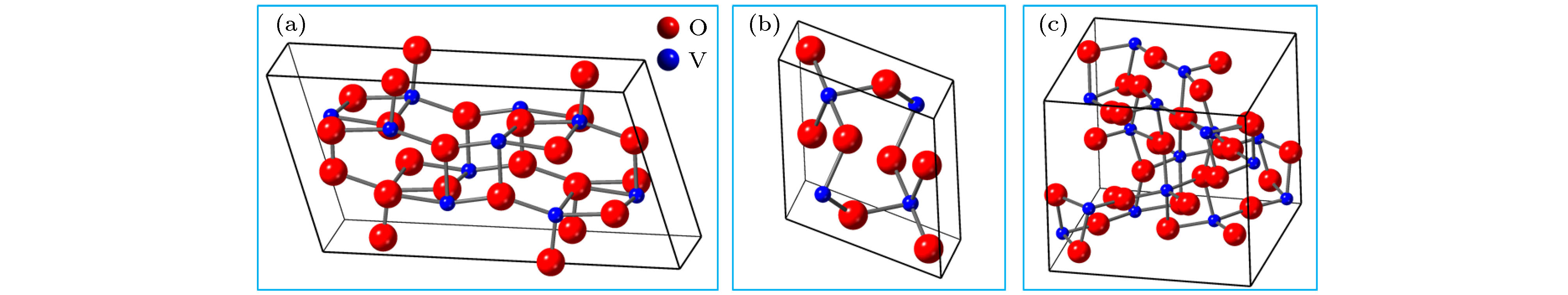
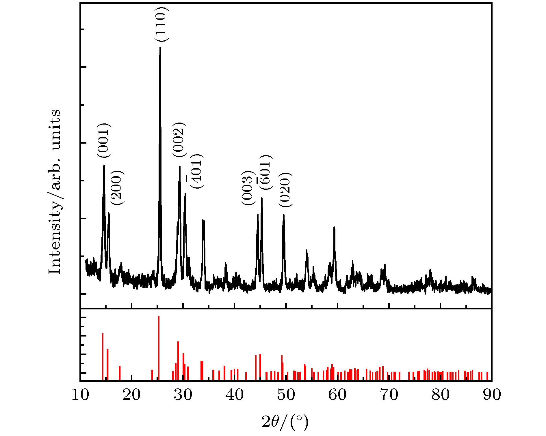
图 1 VO2晶体结构图 (a) B相; (b) M相; (c) R相.
Fig. 1. Crystal structure diagrams of VO2: (a) B phase; (b) M phase; (c) R phase
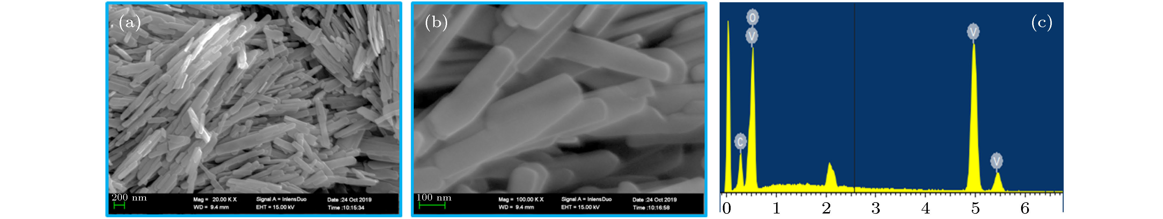
图 3 VO2 (B) 颗粒SEM图 (a) 放大倍率为2万倍; (b) 放大倍率为10万倍; (c) X射线能谱分析图
Fig. 3. SEM images of VO2 (B) particles: (a) The magnification is 20000 times; (b) the magnification is 100000 times; (c) EDS spectrum.
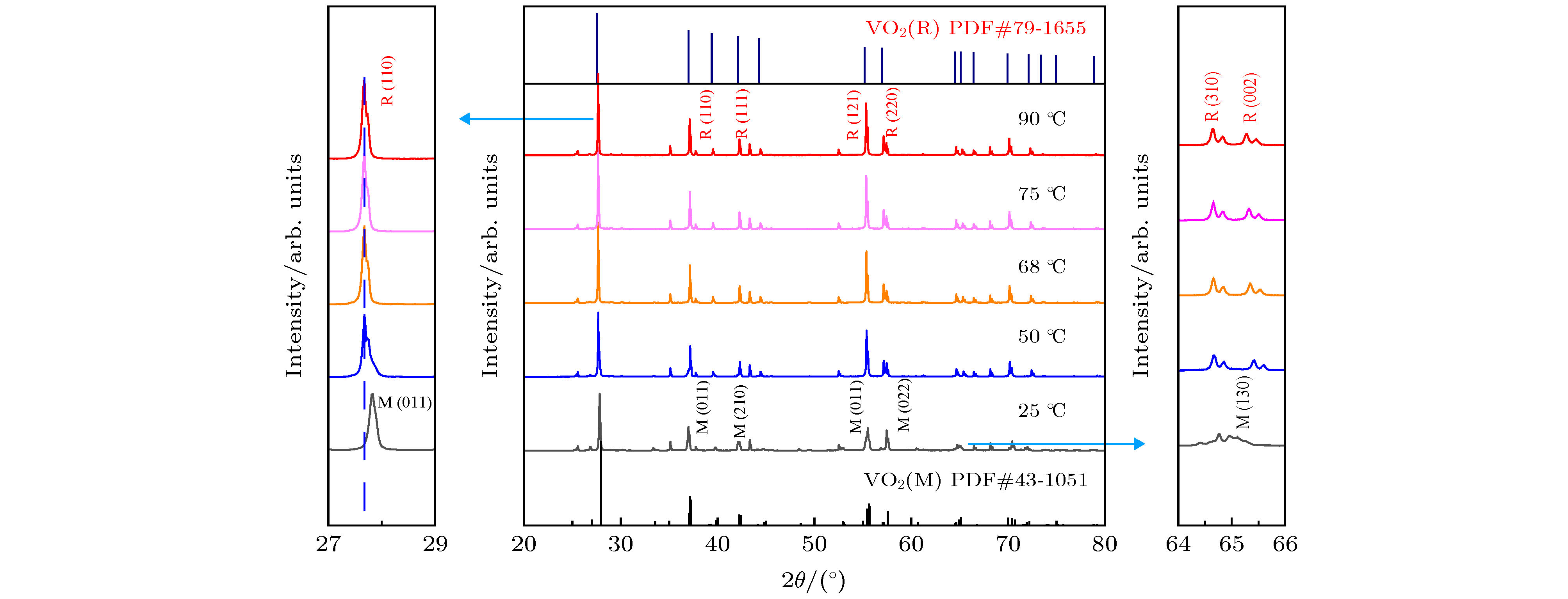
图 5 4#样品(退火时间t = 60 min)的变温XRD曲线
Fig. 5. Variable-temperature XRD patterns of sample 4# (annealing time t = 60 min)
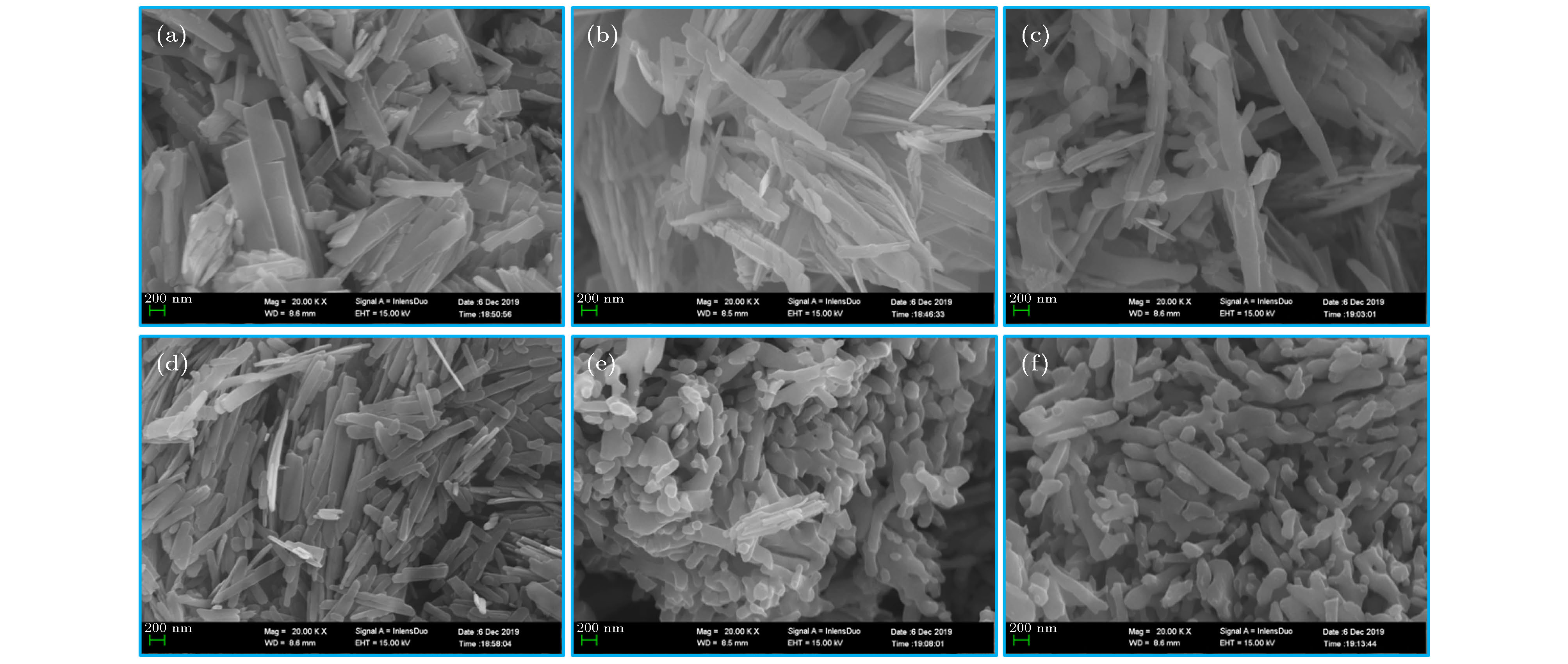
图 6 不同退火时间样品的SEM图 (a)退火时间为5 min; (b)退火时间为20 min; (c)退火时间为30 min; (d)退火时间为60 min; (e)退火时间为90 min; (f)退火时间为300 min
Fig. 6. SEM images of samples with different annealing times: (a) Annealing time is 5 min; (b) annealing time is 20 min; (c) annealing time is 30 min; (d) annealing time is 60 min; (e) annealing time is 90 min; (f) annealing time is 300 min
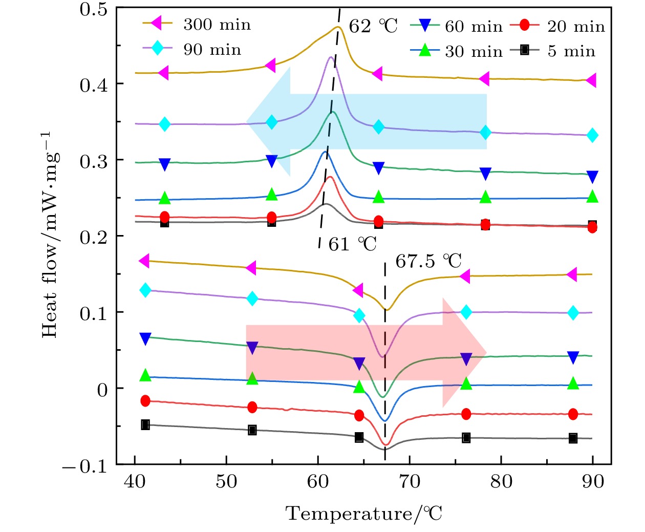
图 7 不同退火时间制备样品的DSC测试曲线(下半部分为升温曲线, 上半部分为降温曲线)
Fig. 7. DSC curves of samples prepared at different annealing times (The lower is the heating curves, and the upper is the cooling curves)
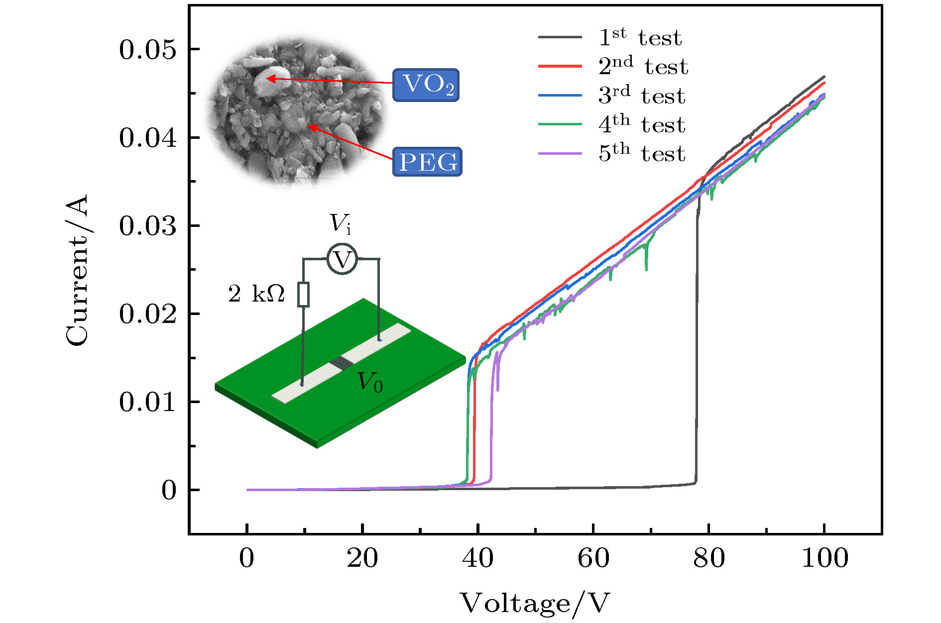
图 8 VO2-PEG复合薄膜V-I曲线(下插图为测试连接示意图(两电极之间间距为1 mm, 电极宽度为2 mm), 上插图为薄膜SEM图)
Fig. 8. V-I curves of VO2-PEG composite film. The inset at the bottom is the schematic diagram of the test connection (The distance between the two electrodes is 1 mm, and the electrode width is 2 mm), and the inset at the top is the SEM image of the film.
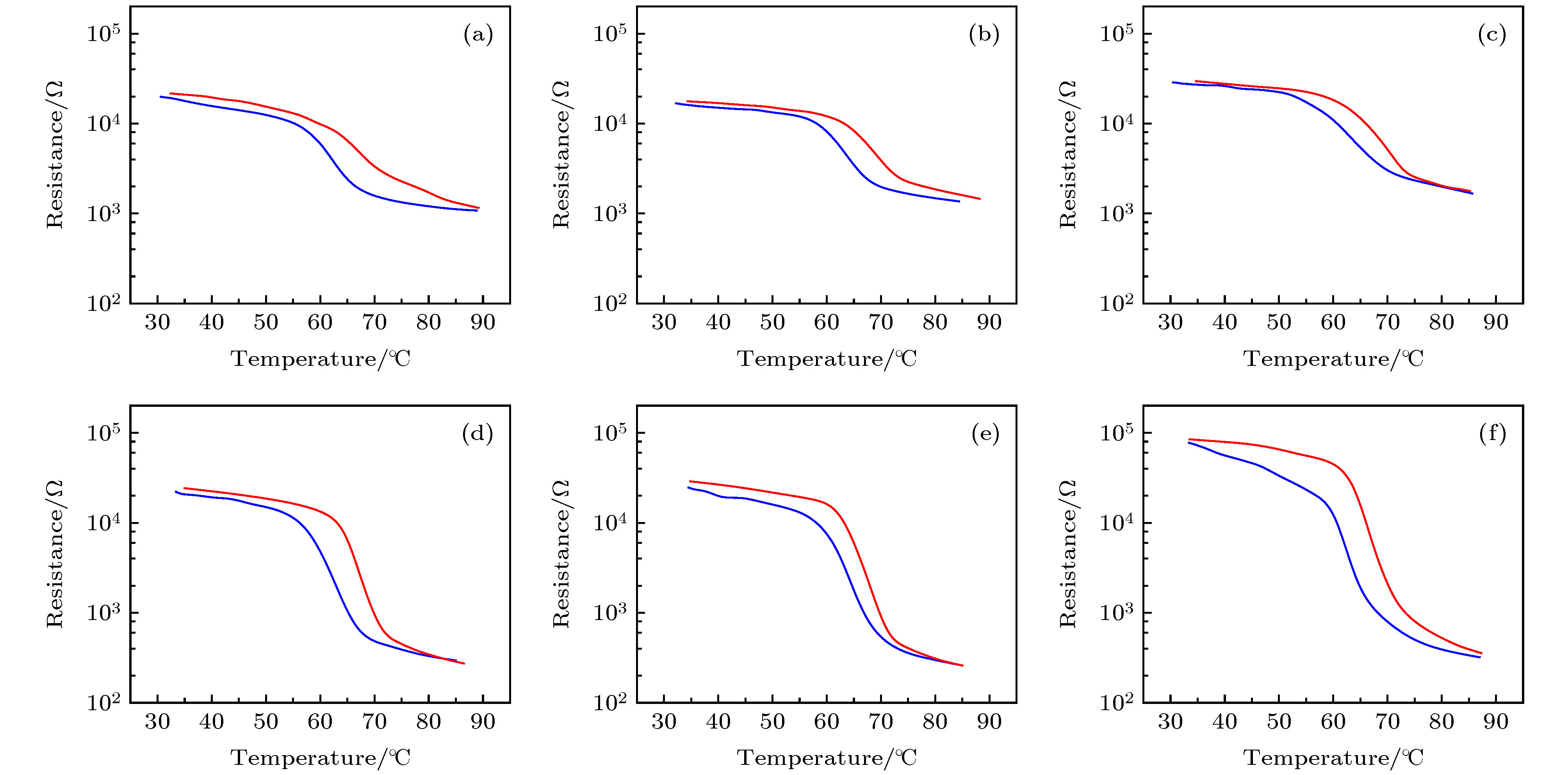
图 9 (a)−(f)样品1#−6#的变温电阻曲线(红色为升温曲线, 蓝色为降温曲线)
Fig. 9. Temperature-dependent resistance curves of (a)−(f) samples 1#−6# (The red lines are the heating curves; the blue lines are the cooling curves).

图 10 复合薄膜典型测试曲线分析图 (a)输入电压Vi与电流I曲线; (b)输入电压Vi与材料电阻R0曲线; (c)材料两端电压V0与电流I曲线; (d)输入电压Vi与材料两端电压V0曲线
Fig. 10. Analysis of the second test curve of the composite film: (a) Input voltage Vi vs. current I; (b) input voltage Vi vs. material resistance R0 curve; (c) voltage across the material V0 vs. current I curve; (d) input voltage Vi vs. voltage across the material V0 curve
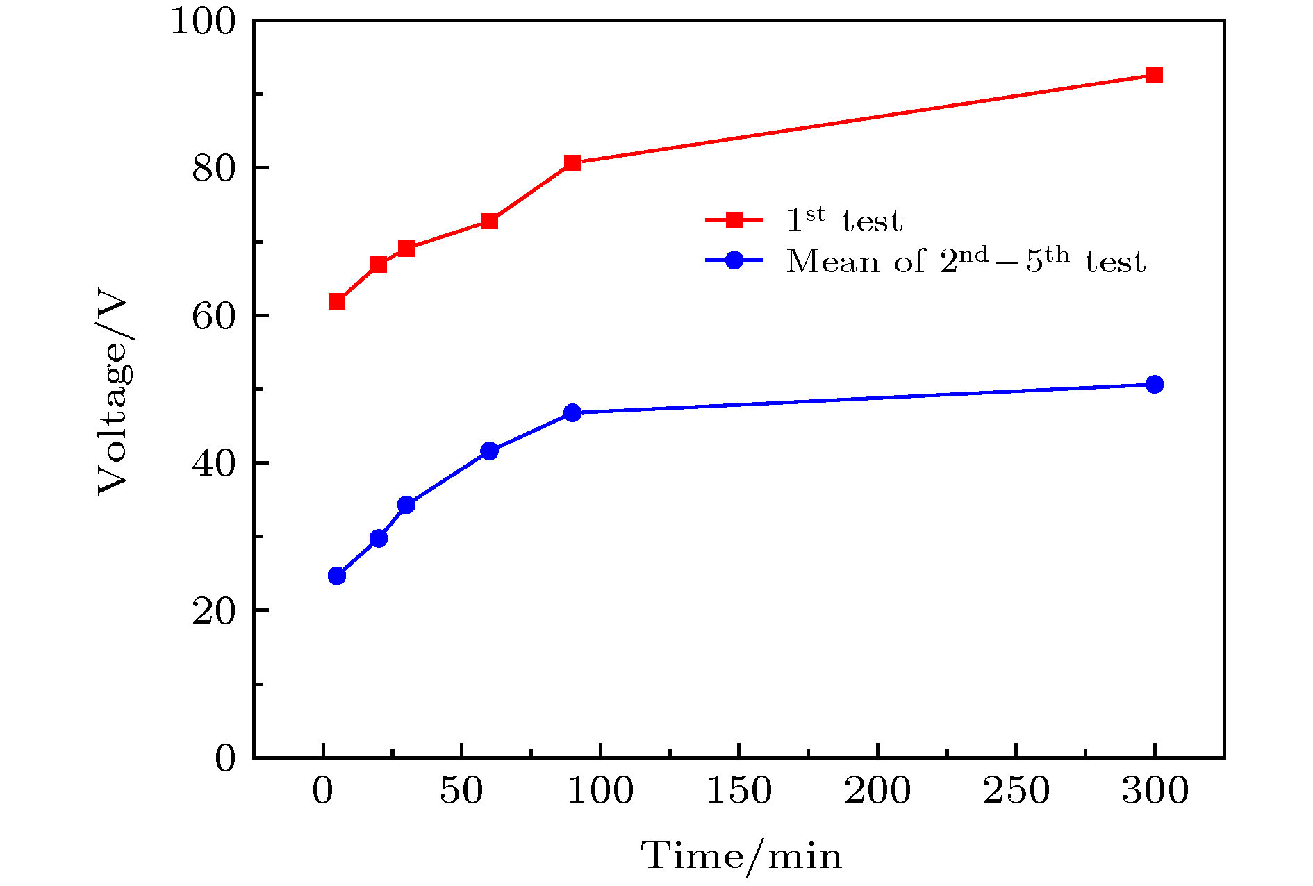
图 11 不同退火时间样品的相变电压变化曲线
Fig. 11. MIT voltage curves of samples with different annealing times.
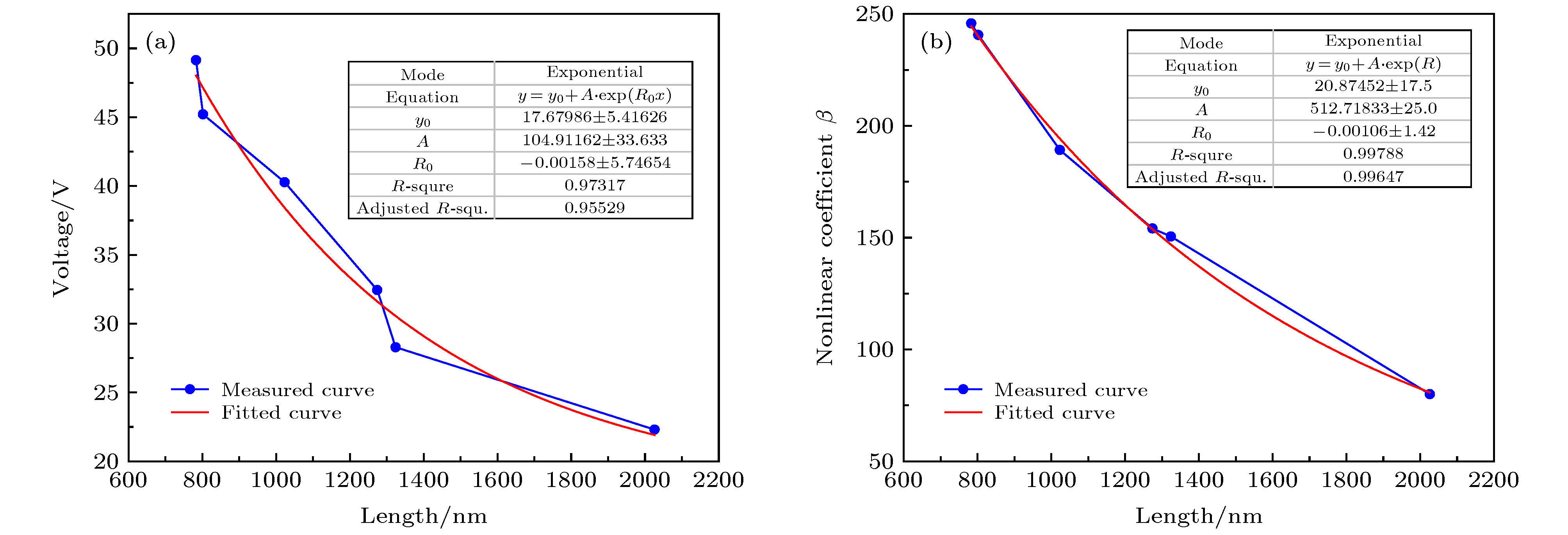
图 12 相变电压(a)及非线性系数(b)随纳米颗粒长度的变化曲线(红色为拟合曲线)
Fig. 12. MIT voltage (a) and nonlinear coefficient (b) with the nanoparticle length change curves (The red lines are the fitting curves).
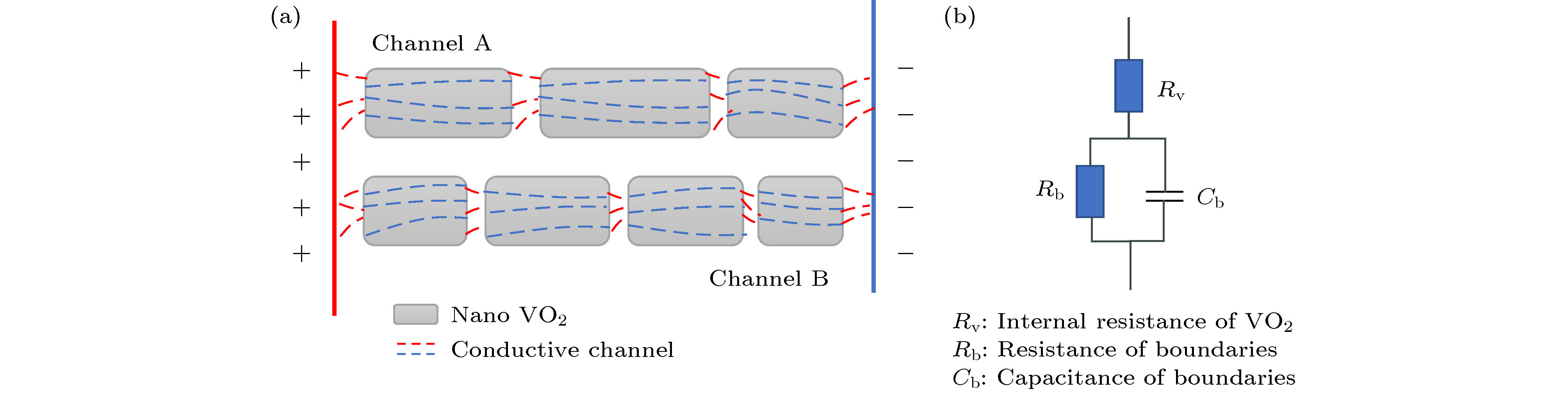
图 13 VO2复合薄膜中导电通道模型(a)和电路简化模型(b)
Fig. 13. The conductive channel model (a) and the simplified circuit model (b) in the VO2 composite film.
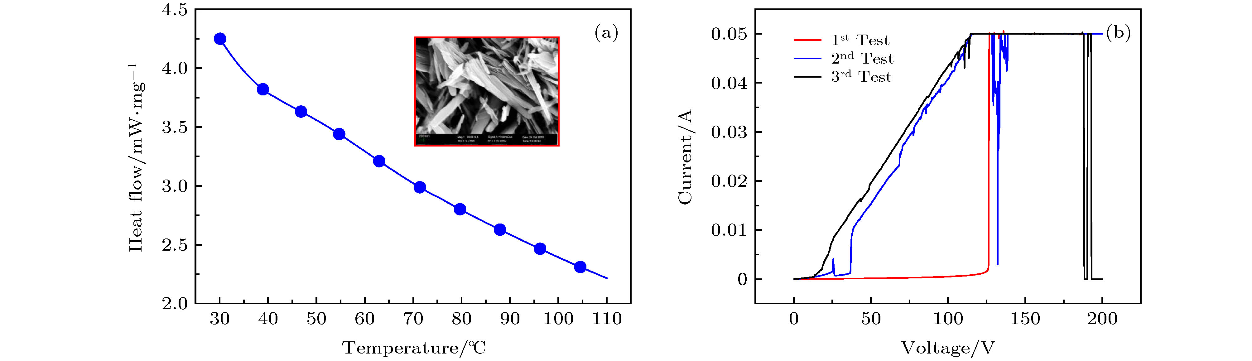
图 14 对比样品DSC曲线(插图为样品7#SEM图) (a)和 V-I测试曲线 (b)
Fig. 14. DSC curve (a) of the comparative sample (the inset is the SEM of sample 7#) and the V-I test curves (b).
表 1 不同退火时间薄膜的电压响应数据表
Table 1. Voltage response data table of films with different annealing times.
Annealing
time/minLength of VO2
belt/nmNonlinear
coefficient$ {R}_{0}^{1} $ at Vi = 5 V/kΩ $ {R}_{0}^{2} $ at Vi = 100 V/Ω Limit voltage/V 1# 5 2026 79.97 80.33 362.66 12.71 2# 20 1324 150.50 119.99 208.63 8.88 3# 30 1274 154.11 105.66 225.65 9.16 4# 60 1023 189.19 114.80 224.00 11.30 5# 90 802 240.64 77.60 236.93 10.23 6# 300 783 245.79 94.33 231.48 10.56  下载: 导出CSV
-
[1] Surnev S, Ramsey M G, Netzer F P 2003 Prog. Surf. Sci. 73 117
Google Scholar
[2] Stefanovich G, Pergament A, Stefanovich D 2000 J. Phys. Condens. Matter 12 8837
Google Scholar
[3] Karakotsou C, Anagnostopoulos A N, Kambas K, Spyridelis J 1992 Phys. Rev. B 46 16144
Google Scholar
[4] Morin F J 1959 Phys. Rev. Lett. 3 34
Google Scholar
[5] 王庆国, 何长安, 曲兆明, 山世浩, 李昂, 成伟, 王妍 2018 安全与电磁兼容 2018 14
Wang Q G, He C A, Qu Z M, Shan S H, Li A, Cheng W, Wang Y 2018 Safety & EMC 2018 14
[6] Yang Z, Ko C, Ramanathan S 2011 Annu. Rev. Mater. Res. 41 337
Google Scholar
[7] Becker M F, Buckman A B, Walser R M, Lépine T, Georges P, Brun A 1996 J. Appl. Phys. 79 2404
Google Scholar
[8] Ji S, Zhao Y, Zhang F, Jin P 2010 J. Cryst. Growth 312 282
Google Scholar
[9] Zhang Y, Zhang J, Zhang X, Mo S, Wu W, Niu F, Zhong Y, Liu X, Huang C, Liu X 2013 J. Alloys Compd. 570 104
Google Scholar
[10] Zhang K F, Bao S J, Liu X, Shi J, Su Z X, Li H L 2006 Mater. Res. Bull. 41 1985
Google Scholar
[11] Song Z D, Zhang L M, Xia F, Webster N A, Song J, Liu B, Luo H, Gao Y 2016 Inorg. Chem. Front. 3 1035
Google Scholar
[12] Ji S, Zhang F, Jin P 2011 J. Solid State Chem. 184 2285
Google Scholar
[13] 张娇, 李毅, 刘志敏, 李政鹏, 黄雅琴, 裴江恒, 方宝英, 王晓华, 肖寒 2017 物理学报 66 238101
Google Scholar
Zhang J, Li Y, Liu Z M, Li Z P, Huang Y Q, Pei J H, Fang B Y, Wang X H, Xiao H 2017 Acta Phys. Sin. 66 238101
Google Scholar
[14] 覃源, 李毅, 方宝英, 佟国香, 王晓华, 丁杰, 王峰, 严梦, 梁倩, 陈少娟 2013 光学学报 33 343
Google Scholar
Qin Y, Li Y, Fang B Y, Tong G X, Wang X H, Ding J, Wang F, Yan M, Liang Q, Chen S J 2013 Acta Opt. Sin. 33 343
Google Scholar
[15] Chen L, Wang X, Wan D, Cui Y, Liu B, Shi S, Luo H, Gao Y 2016 RSC Adv. 6 73070
Google Scholar
[16] Ji S, Zhang F, Jin P 2011 Sol. Energy Mater. Sol. Cells 95 3520
Google Scholar
[17] Rathi S, Lee I y, Park J H, Kim B J, Kim H T, Kim G H 2014 ACS Appl. Mater. Interfaces 6 19718
Google Scholar
[18] Kozo T, Li Z C, Wang Y Q, Ni J, Hu Y, Zhang Z J 2009 Front. Mater. Sci. Chin. 3 48
Google Scholar
[19] Kumar M, Singh J P, Chae K H, Park J, Lee H H 2020 Superlattices Microstruct. 137 106335
Google Scholar
[20] Meng Y F, Sang J X, Liu Z, Xu X F, Tan Z Y, Wang C R, Wu B H, Wang C, Cao J C, Chen X S 2019 Appl. Surf. Sci. 470 168
Google Scholar
[21] Rathi S, Park J H, Lee I, Jin Kim M, Min Baik J, Kim G H 2013 Appl. Phys. Lett. 103 203114
Google Scholar
[22] Xu H Y, Huang Y H, Liu S, Xu K W, Ma F, Chu P K 2016 RSC Adv. 137 79383
Google Scholar
[23] Afify H H, Hassan S A, Obaida M, Abouelsayed A 2019 Physica E 114 113610
Google Scholar
[24] 罗明海, 徐马记, 黄其伟, 李派, 何云斌 2016 物理学报 65 047201
Google Scholar
Luo M H, Xu M J, Huang Q W, Li P, He Y B 2016 Acta Phys. Sin. 65 047201
Google Scholar
[25] Dai L, Cao C, Gao Y, Luo H 2011 Sol. Energy Mater. Sol. Cells 95 712
Google Scholar
[26] Wu C, Zhang X, Dai J, Yang J, Wu Z, Wei S, Xie Y 2011 J. Mater. Chem. 21 4509
Google Scholar
[27] Antonova K V, Kolbunov V R, Tonkoshkur A S 2014 J. Polym. Res. 21 422
Google Scholar
[28] Pillai S C, Kelly J M, Ramesh R, McCormack D E 2013 J. Mater. Chem. C 1 3268
Google Scholar
[29] Qazilbash M M, Brehm M, Chae B G, Ho P C, Andreev G O, Kim B J, Yun S J, Balatsky A V, Maple M B, Keilmann F, Kim H T, Basov D N 2007 Science 318 1750
Google Scholar
[30] Zylbersztejn A, Mott N F 1975 Phys. Rev. B 11 4383
Google Scholar
[31] Gervais F, Kress W 1985 Phys. Rev. B 31 4809
Google Scholar
[32] 孙肖宁, 曲兆明, 王庆国, 袁扬, 刘尚合 2019 物理学报 68 107201
Google Scholar
Sun X N, Qu Z M, Wang Q G, Yuan Y, Liu S H 2019 Acta Phys. Sin. 68 107201
Google Scholar
[33] Rozen J, Lopez R, Haglund R F, Feldman L C 2006 Appl. Phys. Lett. 88 081902
Google Scholar
[34] He X F, Xu J, Xu X F, Gu C C, Chen F, Wu B H, Wang C R, Xing H Z, Chen X S, Chu J H 2015 Appl. Phys. Lett. 106 093106
Google Scholar
[35] Kumar S, Pickett M D, Strachan J P, Gibson G, Nishi Y, Williams R S 2013 Adv. Mater. 25 6128
Google Scholar
[36] Singh S, Horrocks G, Marley P M, Shi Z, Banerjee S, Sambandamurthy G 2015 Phys. Rev. B 92 155121
Google Scholar
[37] Joushaghani A, Jeong J, Paradis S, Alain D, Stewart Aitchison J, Poon J K S 2014 Appl. Phys. Lett. 105 231904
Google Scholar
[38] Zeng W, Chen N, Xie W G 2020 Cryst. Eng. Comm. 22 851
Google Scholar
[39] Whittaker L, Jaye C, Fu Z, Fischer D A, Banerjee S 2009 J. Am. Chem. Soc. 131 8884
Google Scholar
[40] Wang Z S, Zeng F, Yang J, Chen C, Pan F 2012 ACS Appl. Mater. Interfaces 4 447
Google Scholar
[41] Mamunya E P, Davidenko V V, Lebedev E V 1996 Compos. Interfaces 4 169
Google Scholar
[42] Yang W, Wang J, Luo S, Yu S, Huang H, Sun R, Wong C P 2016 ACS Appl. Mater. Interfaces 8 35545
Google Scholar

 下载:
下载:

计量
- 文章访问数: 9082
- PDF下载量: 112
- 被引次数: 0
