


-
The rapid development of the electrical and electronic industry requires components with miniaturization, flexibility, and intelligence. Dielectric materials, as important materials for the preparation of electronic components, are required to have excellent dielectric properties such as high breakdown electric field, high energy storage density and low dielectric loss. Owing to the lack of ultra-high resolution characterization tools, the research on the improvement of dielectric material properties stopped at a macroscopic level in the past. Atomic force microscopy, a measurement instrument which possesses a nanoscale high resolution, shows unique advantages in the study of nanodielectrics, and the advent of functional atomic force microscopy has made important contributions to characterization of the electrical, optical, and mechanical properties of nano-dielectric micro-regions. In this paper, we review the progress of atomic force microscopy, electrostatic force microscopy, Kelvin probe force microscopy, piezoelectric response force microscopy and atomic microscopy-infrared spectroscopy in the study of nanodielectric applications. Firstly, their structures and principles are introduced; secondly, their recent research progress of studying the microscopic morphology, interfacial structure, domain behavior and charge distribution in the nanometer region of dielectric materials is presented, and finally, the problems in the existing research and possible future research directions are discussed.
-
Keywords:
- atomic force microscopy /
- nano dielectric /
- interface /
- dielectric properties
[1] Lewis T J 1994 IEEE Trans. Dielectr. Electr. Insul. 1 812
 Google Scholar
[2] Frechette M F, Trudeau M L, Alamdar H, Boily S 2004 IEEE Trans. Dielectr. Electr. Insul. 11 808
Google Scholar
[3] Nelson J K, Fothergill J C, Dissado L A, Peasgood W 2002 Annual Report Conference on Electrical Insulation and Dielectric Phenomena Cancun, Mexico, October 20–24 2002 p295
[4] Nelson J K, Fothergill J C 2004 Nanotechnology 15 586
Google Scholar
[5] 王娇, 刘少辉, 陈长青, 郝好山, 翟继卫 2020 物理学报 69 217702
Google Scholar
Wang J, Liu S H, Chen C Q, Hao H S, Zhai J W 2020 Acta Phys. Sin. 69 217702
Google Scholar
[6] Lau K Y, Vaughan A S, Chen G 2015 IEEE Electr. Insul. Mag. 31 45
Google Scholar
[7] Wang B K, Barbiero M, Zhang Q M, Gu M 2019 Front. Inform. Tech. El. 20 608
Google Scholar
[8] Sun C, Müller E, Meffert M, Gerthsen D 2018 Microsc. Microanal. 24 99
Google Scholar
[9] Binnig G, Quate C F, Gerber C 1986 Phys. Rev. Lett. 56 930
Google Scholar
[10] Schmitz I, Schreiner M, Friedbacher G, Grasserbauer M 1997 Appl. Surf. Sci. 115 190
Google Scholar
[11] Binnig G, Rohrer H 1983 Surf, Sci. 126 236
[12] Martin Y, Williams C C, Wickramasinghe H K 1987 J. Appl. Phys. 61 4723
Google Scholar
[13] Zhong Q, Inniss D, Kjoller K, Elings V B 1993 Surf Sci. 290 L688
[14] Handschuh-Wang S, Wang T, Zhou X 2017 RSC Adv. 7 47464
Google Scholar
[15] Girard P 2001 Nanotechnology 12 485
Google Scholar
[16] Nonnenmacher M, Oboyle M P, Wickramasinghe H K 1991 Appl. Phys. Lett. 58 2921
Google Scholar
[17] Güthner P, Dransfeld K 1992 Appl. Phys. Lett. 61 1137
Google Scholar
[18] Gruverman A 1996 J. Vac. Sci. Technol. B. 14 602
Google Scholar
[19] Kalinin S V, Rodriguez B J, Jesse S, Karapetian E, Mirman B, Eliseev E A, Morozovska A N 2007 Annu. Rev. Mater. Res. 37 189
Google Scholar
[20] Dazzi A, Prater C B 2017 Chem. Rev. 117 5146
Google Scholar
[21] Singh A, Guha P, Panwar A K, Tyagi P K 2017 Appl. Surf. Sci. 402 271
Google Scholar
[22] El Khoury D, Fedorenko V, Castellon J, Bechelany M, Laurentie J C, Balme S, Fréchette M, Ramonda M, Arinero R 2017 Scanning 2017 1
[23] Zhao W, Cui W, Xu S, Wang Y, Zhang K, Wang D, Cheong L Z, Besenbacher F, Shen C 2018 Ultramicroscopy 196 24
[24] Sharma A, Basu S, Gupta N 2020 IEEE Trans. Dielectr. Electr. Insul. 27 866
Google Scholar
[25] Jones J T, Bridger P M, Marsh O J, Mcgill T C 1999 Appl. Phys. Lett. 75 1326
[26] Kelley T W, Granstrom E, Frisbie C D 1999 Adv. Mater. 11 261
Google Scholar
[27] Rosenberger M R, Chuang H J, Phillips M, Oleshko V P, McCreary K M, Sivaram S V, Hellberg C S, Jonker B T 2020 ACS Nano 14 4550
Google Scholar
[28] Lanza M, Celano U, Miao F 2017 J. Electroceram. 39 94
Google Scholar
[29] Li R, Taniguchi T, Watanabe K, Xue J 2020 Rev. Sci. Instrum. 91 073702
Google Scholar
[30] Glatzel T, Gysin U, Meyer E 2022 Microscopy 71 i165
[31] Faliya K, Kliem H, Dias C J 2017 IEEE Trans. Dielectr. Electr. Insul. 24 1913
Google Scholar
[32] Iglesias V, Lanza M, Zhang K, Bayerl A, Porti M, Nafría M, Aymerich X, Benstetter G, Shen Z Y, Bersuker G 2011 Appl. Phys. Lett. 99 103510
Google Scholar
[33] Proksch R, Nanophase C F, Sciences M, Kalinin S https://afm.oxinst.cn/assets/uploads/products/asylum/documents/Piezoresponse-Force-Microscopy-PFM-AFM.pdf [2022-5-27]
[34] Döring J, Eng L M, Kehr S C 2016 J. Appl. Phys. 120 084103
Google Scholar
[35] Eng L M 1999 Nanotechnology 10 405
Google Scholar
[36] Kalinin S V, Rodriguez B J, Jesse S, Shin J, Baddorf A P, Gupta P, Jain H, Williams D B, Gruverman A 2006 Microsc. Microanal. 12 206
Google Scholar
[37] McQuaid R G, McGilly L J, Sharma P, Gruverman A, Gregg J M 2011 Nat Commun 2 404
Google Scholar
[38] Matey J R, Blanc J 1985 J. Appl. Phys. 57 1437
Google Scholar
[39] Lee D T, Pelz J P, Bhushan B 2006 Nanotechnology 17 1484
Google Scholar
[40] Szyszka A, Dawidowski W, Stafiniak A, Prażmowska J, Ściana B, Tłaczała M 2017 Cryst. Res. Technol. 52 1700019
Google Scholar
[41] Hong J W, Shin S M, Kang C J, Kuk Y, Park S I 1999 Appl. Phys. Lett. 75 1760
Google Scholar
[42] Lu F, Jin M, Belkin M A 2014 Nat. Photonics 8 307
Google Scholar
[43] Tang F, Bao P, Su Z 2016 Anal. Chem. 88 4926
Google Scholar
[44] Marcott C, Lo M, Kjoller K, Prater C, Noda I 2011 Appl. Spectrosc. 65 1145
Google Scholar
[45] Dazzi A, Prater C B, Hu Q, Chase D B, Rabolt J F, Marcott C 2012 Appl. Spectrosc. 66 1365
Google Scholar
[46] Fernandes J P C, Mareau V H, Gonon L 2017 Int. J. Polym. Anal. Charact. 23 113
[47] Surtchev M, Magonov S, Zayats S, Wall M https://assets.thermofisher.com/TFS-Assets/CAD/Application-Notes/AN52664-Characterization-Polymer-Blends-Raman-AFM-2015.pdf [2022-6-28]
[48] Schmidt U, Dieing T, Weishaupt K, Liu W, Yang J 2012 Microsc. Microanal. 18 1504
Google Scholar
[49] Schmidt U, Liu W, Yang J, Dieing T, Weishaupt K 2015 Microsc. Microanal. 21 2189
Google Scholar
[50] Troyon M, Wang Z, Pastre D, Lei H, Hazotte A 1997 Nanotechnology 8 163
Google Scholar
[51] Radmacher M, Tillmann R, Gaub H 1993 Biophys. J. 64 735
Google Scholar
[52] Price W J, Leigh S A, Hsu S M, Patten T E, Liu G Y 2006 J. Phys. Chem. A 110 1382
Google Scholar
[53] Maivald P, Butt H, Gould S, Prater C, Drake B, Gurley J, Elings V, Hansma P 1991 Nanotechnology 2 103
Google Scholar
[54] Schwarz U D, KoSter P, Wiesendanger R 1996 Rev. Sci. Instrum. 67 2560
Google Scholar
[55] Yamanaka K, Tomita E 2014 Jpn. J. Appl. Phys. 34 2879
Google Scholar
[56] Weymouth A J, Hofmann T, Giessibl F J 2014 Science 343 1120
Google Scholar
[57] Goddenhenrich T, Muller S, Heiden C 1994 Rev. Sci. Instrum. 65 2870
Google Scholar
[58] Chelakara Satyanarayana K, Bolton K 2012 Polymer 53 2927
Google Scholar
[59] Mohammadi B, Yousefi A A, Bellah S M 2007 Polym. Test. 26 42
Google Scholar
[60] Ye H J, Yang L, Shao W Z, Sun S B, Zhen L 2013 RSC Adv. 3 23730
Google Scholar
[61] Gil H A, Faria R M, Kawano Y 1998 Polym. Degrad. Stab. 61 265
Google Scholar
[62] Tiwari V K, Kulriya P K, Avasthi D K, Maiti P 2009 J. Phys. Chem. B 113 11632
Google Scholar
[63] Ye H J, Yang L, Shao W Z, Li Y, Sun S B, Zhen L 2014 RSC Adv. 4 13525
Google Scholar
[64] Wang M, Wang S, Hu J, Li H, Ren Z, Sun X, Wang H, Yan S 2020 Macromolecules 53 5971
Google Scholar
[65] Gregorio R 2006 J. Appl. Polym. Sci. 100 3272
Google Scholar
[66] Gregorio R, Capitao R 2000 J. Mater. Sci. 35 299
Google Scholar
[67] Li W, Meng Q, Zheng Y, Zhang Z, Xia W, Xu Z 2010 Appl. Phys. Lett. 96 334
[68] Lovinger A J 1980 Polymer 21 1317
Google Scholar
[69] Prest W M, Luca D J 1978 J. Appl. Phys. 49 5042
Google Scholar
[70] Ghosh S K, Rahman W, Middya T R, Sen S, Mandal D 2016 Nanotechnology 27 215401
Google Scholar
[71] Barrau S, Ferri A, Da Costa A, Defebvin J, Leroy S, Desfeux R, Lefebvre J M 2018 ACS Appl. Mater. Interfaces 10 13092
Google Scholar
[72] Thakur Y, Zhang T, Iacob C, Yang T, Bernholc J, Chen L Q, Runt J, Zhang Q M 2017 Nanoscale 9 10992
Google Scholar
[73] Dang Z M, Yuan J K, Yao S H, Liao R J 2013 Adv. Mater. 25 6334
Google Scholar
[74] Li H, Yang T, Zhou Y, Ai D, Yao B, Liu Y, Li L, Chen L Q, Wang Q 2020 Adv. Funct. Mater. 31 2006739
[75] Wang R, Xu H, Cheng S, Liang J, Gou B, Zhou J, Fu J, Xie C, He J, Li Q 2022 Energy Storage Mater. 49 339
Google Scholar
[76] Moharana S, Sai S, Mahaling R N 2018 J. Adv. Dielectr. 08 1850017
[77] 王娇, 刘少辉, 周梦, 郝好山, 翟继卫 2020 物理学报 69 218101
Google Scholar
Wang J, Liu S H, Zhou M, Hao H S, Zhai J W 2020 Acta Phys. Sin. 69 218101
Google Scholar
[78] Chen Z, Shen Z, Liu Y, Zhang Y, Yan S, Feng R, Zhao T, Zhao G, Xiong C, Dong L 2020 Energy Storage Mater. 33 1
Google Scholar
[79] Yin K, Zhou Z, Schuele D E, Wolak M, Zhu L, Baer E 2016 ACS Appl. Mater. Interfaces 8 13555
Google Scholar
[80] Ponting M, Hiltner A, Baer E 2010 Macromol. Symp. 294 19
Google Scholar
[81] Wolak M A, Wan A S, Shirk J S, Mackey M, Hiltner A, Baer E 2012 J. Appl. Polym. Sci. 123 2548
Google Scholar
[82] Tang S, Zhou Z, Mackey M, Carr J M, Mu R, Flandin L, Schuele D E, Baer E, Lei Z 2014 Polymer 55 8
Google Scholar
[83] Lewis T J 2005 J. Phys. D:Appl. Phys. 38 202
Google Scholar
[84] Tanaka T, Kozako M, Fuse N, Ohki Y 2005 IEEE Trans. Dielectr. Electr. Insul. 12 669
Google Scholar
[85] Kirkpatrick S 1973 Rev. Mod. Phys. 45 574
Google Scholar
[86] Takada T, Hayase Y, Tanaka 2008 IEEE Trans. Dielectr. Electr. Insul. 15 152
Google Scholar
[87] Peng S, Zeng Q, Yang X, Hu J, Qiu X, He J 2016 Sci Rep 6 38978
Google Scholar
[88] Zheng C, Zhang W, Zhao H, Wang X, Sun Z, Yang J 2014 IEEE Trans. Dielectr. Electr. Insul. 21 1493
Google Scholar
[89] Seiler J, Kindersberger J 2014 IEEE Trans. Dielectr. Electr. Insul. 21 537
Google Scholar
[90] Deschler J, Seiler J, Kindersberger J 2017 IEEE Trans. Dielectr. Electr. Insul. 24 1027
Google Scholar
[91] Raetzke S, Kindersberger J 2006 IEEJ Trans. Fundam. Mater. 126 1044
Google Scholar
[92] Raetzke S, Kindersberger J 2010 IEEE Trans. Dielectr. Electr. Insul. 17 607
Google Scholar
[93] Liu Y, Yang T, Zhang B, Williams T, Lin Y T, Li L, Zhou Y, Lu W, Kim S H, Chen L Q, Bernholc J, Wang Q 2020 Adv. Mater. 32 e2005431
Google Scholar
[94] Bi M, Hao Y, Zhang J, Lei M, Bi K 2017 Nanoscale 9 16386
Google Scholar
[95] Mao Y P, Mao S Y, Ye Z G, Xie Z X, Zheng L S 2010 J. Appl. Phys. 108 L515
[96] Peng S, Yang X, Wang S, Zhou Y, Hu J 2019 Adv. Mater. 31 1807722
Google Scholar
[97] Xu K, Sun W, Shao Y, Wei F, Zhang X, Wang W, Li P 2018 Nanotechnol. Rev. 7 605
Google Scholar
[98] Altgilbers L L, Baird J, Freeman B L, Lynch C S, Shkuratov S I 1997 Ferroelectric Materials and Their Properties (Netherlands: Elsevier Science Publishers B.V.) pp329–359
[99] Ursic H, Prah U 2019 Proc. Math. Phys. Eng. Sci. 475 20180782
[100] Nonkumwong J, Ananta S, Srisombat L 2015 Appl. Phys. A 119 891
Google Scholar
[101] Nonkumwong J, Sriboriboon P, Kundhikanjana W, Srisombat L, Ananta S 2018 Integr. Ferroelectr. 187 210
Google Scholar
[102] Kholkin A, Bdikin I, Shvartsman V, Orlova A, Kiselev D, Bogomolov A, Kim S H 2004 MRS Online Proceedings Library 838 205
Google Scholar
[103] Zhu L F, Song A, Zhang B P, Gao X Q, Shan Z H, Zhao G L, Yuan J, Deng D, Shu H, Li J F 2022 J. Mater. Chem. A 10 7382
Google Scholar
[104] Furukawa T 1989 Phase Transit. 18 143
Google Scholar
[105] Ling Q D, Liaw D J, Zhu C, Chan D S H, Kang E T, Neoh K G 2008 Prog. Polym. Sci. 33 917
Google Scholar
[106] Cai R, Nysten B, Hu Z, Jonas A M 2017 Appl. Phys. Lett. 110 202901
Google Scholar
[107] Haque M A, Saif M T 2004 J Microelectromech. Syst. 101 6335
[108] Xiao Z, Poddar S, Ducharme S, Hong X 2013 Appl. Phys. Lett. 103 112903
Google Scholar
[109] Zhang B, Wang Q, Zhang Y, Gao W, Hou Y, Zhang G 2019 Nanoscale 11 18046
Google Scholar
[110] Tao S, Yang W, Cheng Z, Zheng N, Ping Y, Schamiloglu E 2014 Appl. Phys. Lett. 105 082903
Google Scholar
[111] Wang T Y, Zhang B Y, Li D Y, Hou Y C, Zhang G X 2020 Nanotechnology 31 324001
Google Scholar
[112] Xie Q, Liang S, Fu K, Liu L, Huang H, Lü F 2018 IEEE Trans. Dielectr. Electr. Insul. 25 2157
Google Scholar
[113] Wang T, Li X, Zhang B, Li D, Liu J, Zhang G 2022 Sci. China Mater. 65 2884
Google Scholar
[114] Pourrahimi A M, Hoang T A, Liu D, Pallon L K, Gubanski S, Olsson R T, Gedde U W, Hedenqvist M S 2016 Adv. Mater. 28 8651
Google Scholar
[115] Peng S, Luo Z, Wang S, Liang J, Yuan C, Yuan Z, Hu J, He J, Li Q 2020 ACS Appl Mater Interfaces 12 53425
Google Scholar
[116] Watson J, Castro G 2015 J. Mater. Sci. :Mater. Electron. 26 9226
Google Scholar
[117] Zhang T, Chen X, Thakur Y, Lu B, Zhang Q, Runt J, Zhang Q 2020 Sci. Adv. 6 eaax6622
Google Scholar
[118] Yuan C, Zhou Y, Zhu Y, Liang J, Wang S, Peng S, Li Y, Cheng S, Yang M, Hu J, Zhang B, Zeng R, He J, Li Q 2020 Nat Commun 11 3919
Google Scholar
[119] Yuan C, Zhou Y, Zhu Y, Hu S, Liang J, Luo Z, Gao B, Zeng T, Zhang Y, Li J 2022 ACS Sustainable Chem. Eng. 10 8685
Google Scholar
-

图 2 功能化原子力显微镜工作原理示意图 (a) AFM; (b) KPFM; (c) EFM; (d) PFM; (e) AFM-IR
Fig. 2. Schematic diagram of functional AFM working principle: (a) AFM; (b) KPFM; (c) EFM; (d) PFM; (e) AFM-IR.
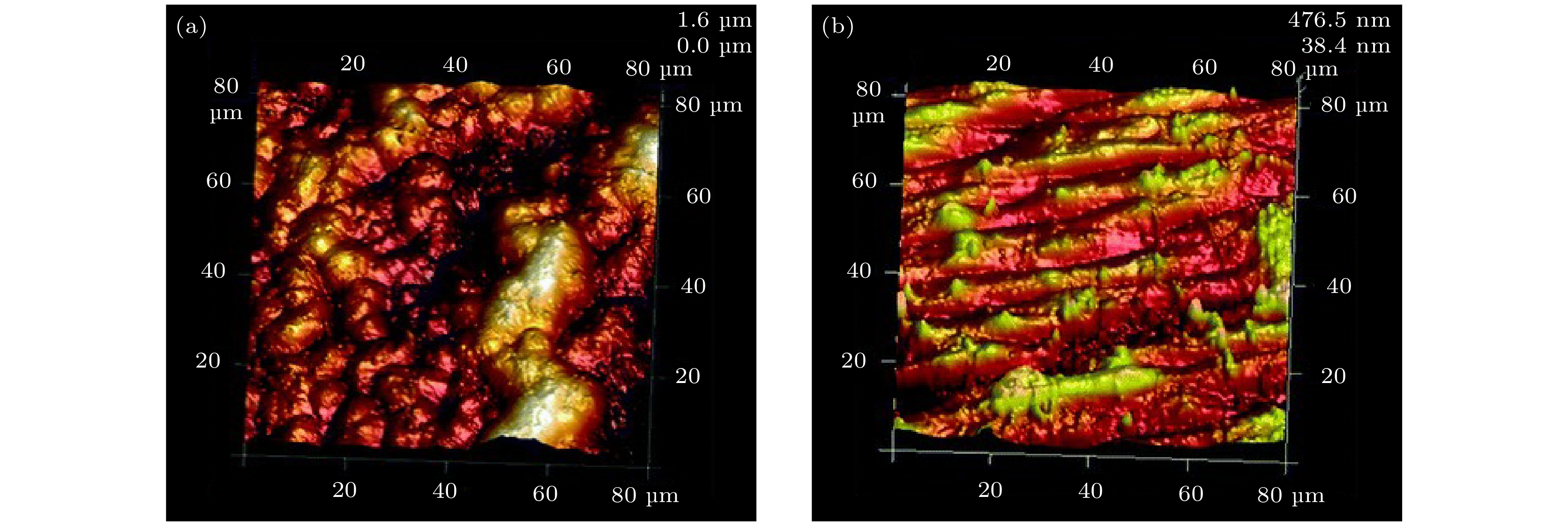
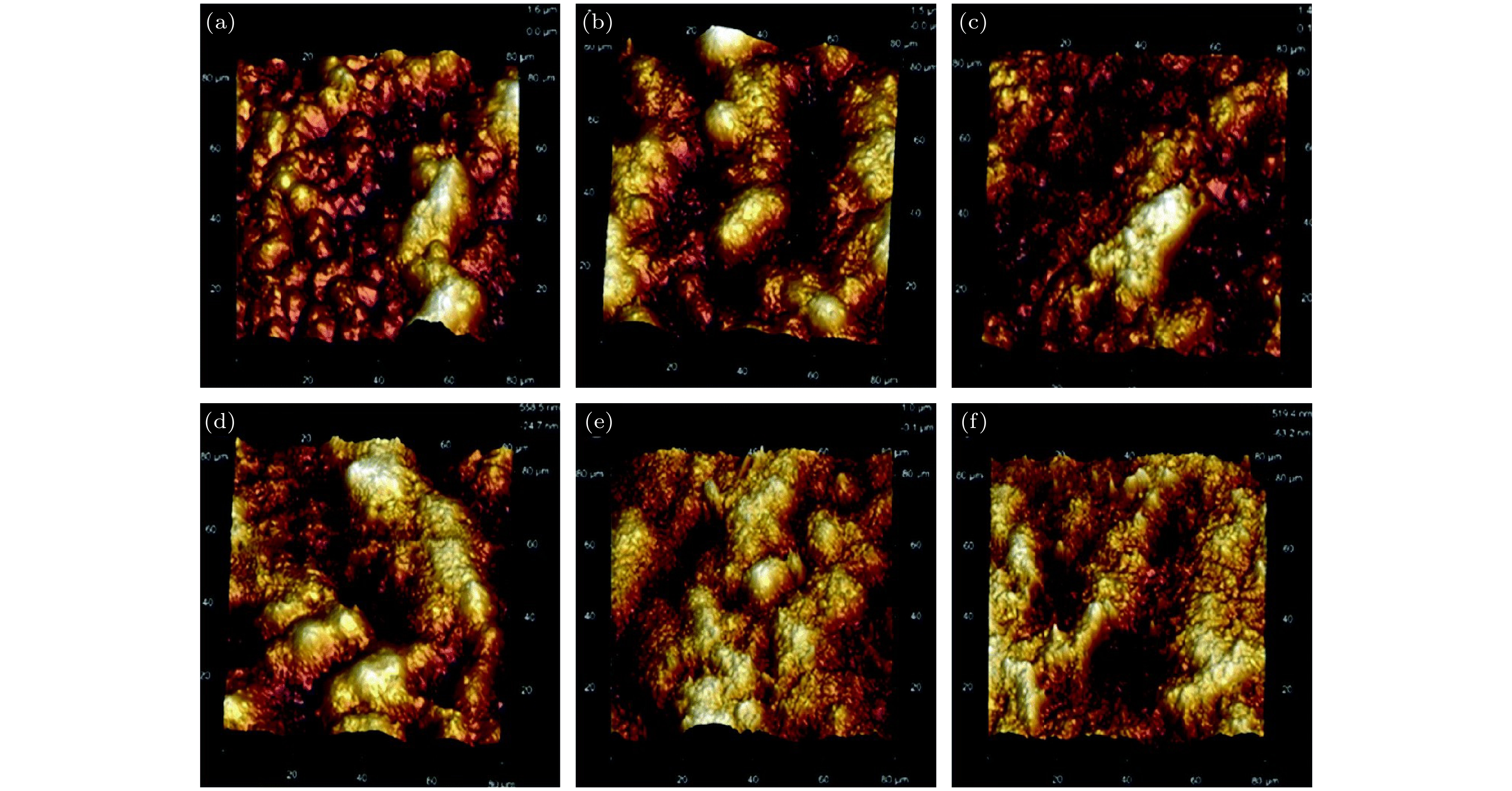

图 5 PVDF样品在加热并保持在162 ℃期间结构演变过程的AFM表征, 其中图(a)—(d)是分别在162 ℃的周期退火(a) 0, (b) 2, (c) 10, (d) 24 h后拍摄[64]; (e) PVDF样品的晶型由α相到γ相的演变过程[64]
Fig. 5. AFM phase images show the structure evolution process of PVDF heating up to and at 162 ℃. The picture was taken after period annealing at 162 ℃ for (a) 0, (b) 2, (c) 10, and (d) 24 h[64]. (e) Scheme showing the crystals evolution of PVDF sample[64].

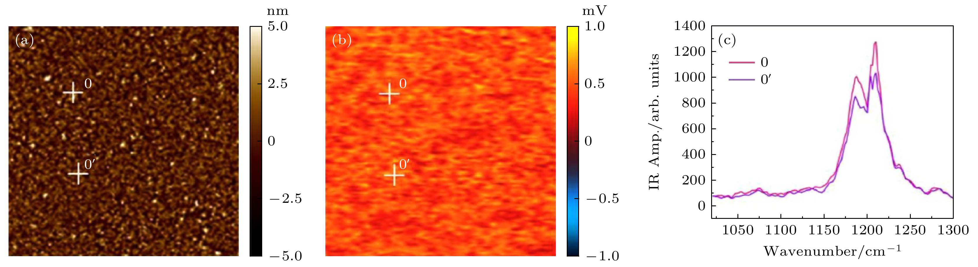
图 7 5% P(VDF-HFP)/GLC的(a) 表面形貌和(b) AFM-IR强度分布[75]; (c) 图(a)和图(b)中标记区域的局部红外光谱[75]
Fig. 7. (a) Topography signal (10 μm×10 μm) and (b) AFM-IR intensity distribution map with irradiation by a laser at 1216 cm–1 of 5% P(VDF-HFP)/GLC[75]; (c) local IR spectra of the sites marked in panel (a) and (b) [75].

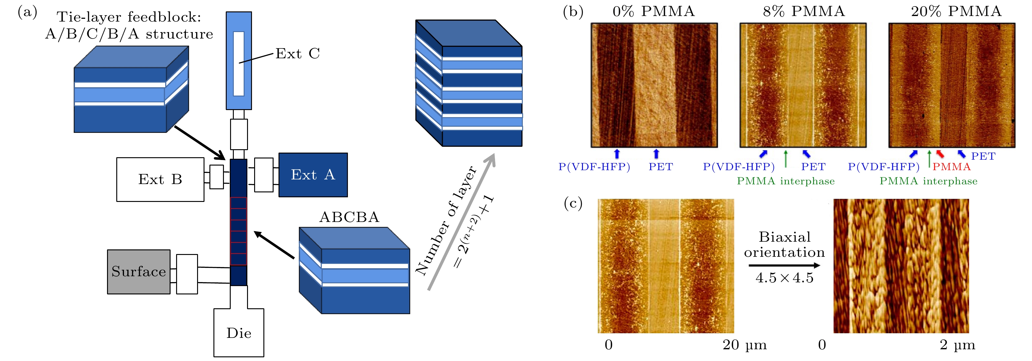
图 9 (a) 强制组装技术进行三组分多层薄膜共挤工艺示意图[79]; (b) PET/PMMA/P(VDF-HFP)多层膜的AFM形貌图[79]; (c) PET/PMMA/P(VDF-HFP)(PMMA的体积分数为8%)65层挤压薄膜(200 μm)和相应的双向拉伸薄膜(10 μm)的AFM形貌图[79]
Fig. 9. (a) Schematics of three-component multilayer film coextrusion process via the forced assembly technique[79]; (b) AFM phase images for PET/PMMA/P(VDF-HFP) multilayer films[79]; (c) AFM phase images of the as-extruded PET/PMMA/P(VDF-HFP) 65-layer film (200 μm) with 8% volume fraction of PMMA and the corresponding biaxially oriented film (10 μm)[79].
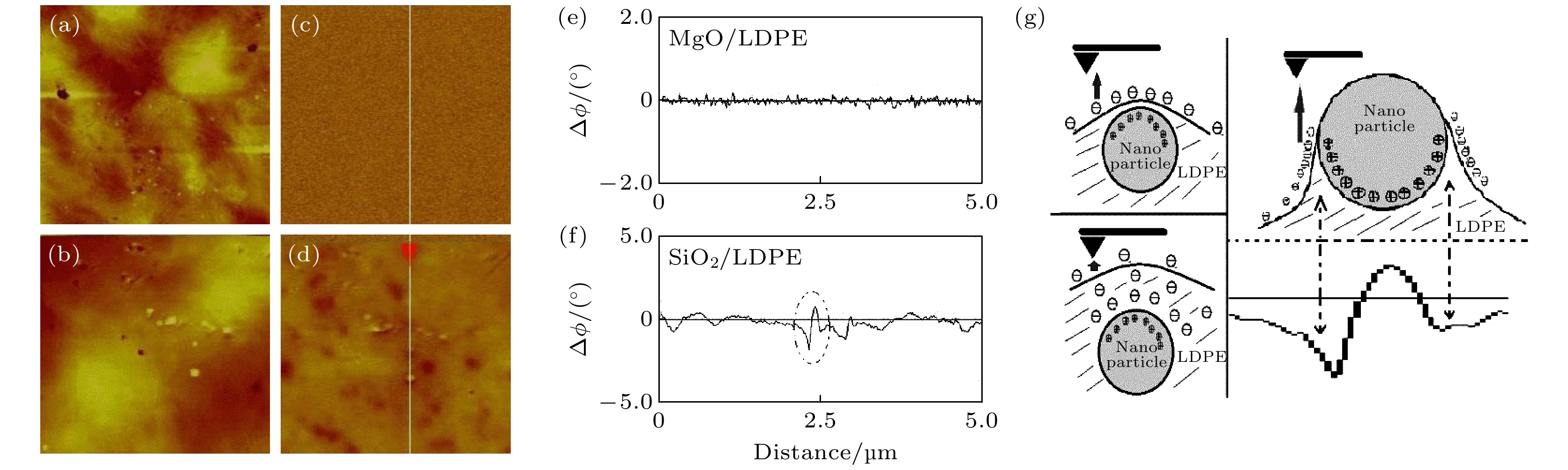
图 12 (a), (b) MgO/LOPE和SiO2/LDPE的AFM高度形貌图(5 μm×5 μm)[88]; (c), (d) MgO/LOPE和SiO2/LDPE的EFM相位图[88]; (e), (f) MgO/LOPE和SiO2/LDPE的一维相位扫描曲线[88]; (g) SiO2在LDPE中不同嵌入形态的模型[88]
Fig. 12. (a), (b) AFM height image of MgO/LOPE and SiO2/LDPE material (5 μm×5 μm)[88]; (c), (d) AFM lift mode phase image of MgO/LOPE and SiO2/LDPE belong to the same zone[88]; (e), (f) scanning curve in one dimension of MgO/LDPE and SiO2/LDPE[88]; (g) models of SiO2 embedded in LDPE[88].
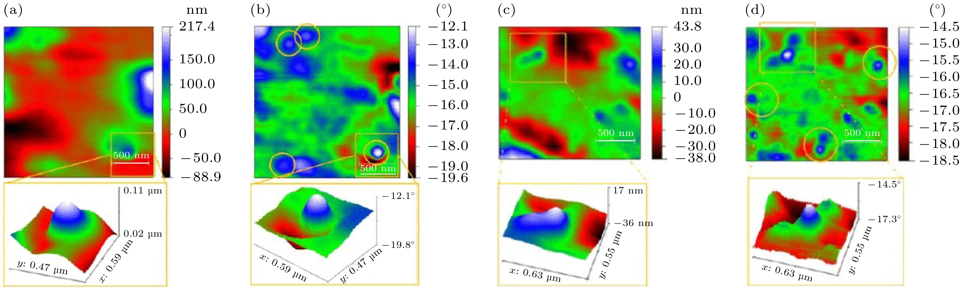
图 13 (a), (b) 含有质量分数为2%的F1填料的有机硅复合材料的AFM形貌图像和EFM图像[89]; (c), (d) 含有质量分数为2%的F2填料的有机硅复合材料的AFM形貌图像和EFM图像[89]
Fig. 13. (a), (b) AFM topography image and EFM image of the silicone composite material containing the filler F1 with mass fraction of 2% [89]; (c), (d) AFM topography image and EFM image of the silicone composite material containing the filler F2 with the mass fraction of 2%[89].
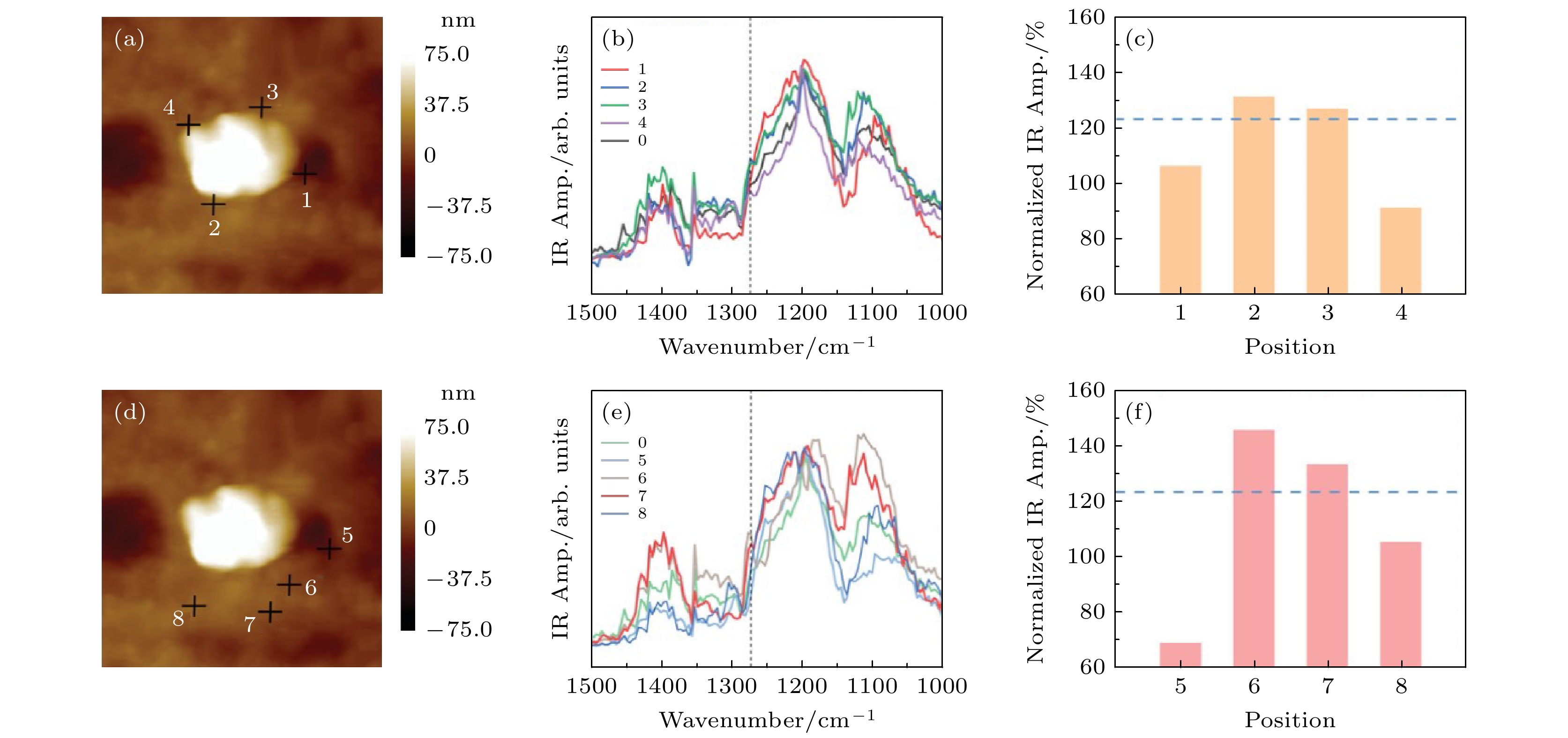
图 14 (a), (d) BTO/P(VDF-TrFE-CFE)的AFM表面高度形貌[93]; (b), (e) 图(a)和(d)中标记位置的局部红外光谱[93]; (c), (f) 图(a)和(d)中标记位置的归一化红外响应[93]
Fig. 14. (a), (d) Topography (1 μm×1 μm) of BTO/P(VDF-TrFE-CFE) nanocomposites[93]; (b), (e) local IR spectra at different sites as marked in panel (a) and (b)[93]; (c), (f) normalized IR response at 1275 cm–1 at different sites as marked in panel (a) and (d)[93]

图 15 (a) 改进KPFM工作原理示意图; (b) P(VDF-TrFE)/BT纳米复合材料界面中氢键和固有偶极子的取向示意图; (c) 不同直流偏压下P(VDF-TrFE)/BT界面附近的局部偏振特性KPFM检测结果[96]; (d) 不同直流电压下的感应表面电位差, 以及偶极层厚度和电势的关系[96]
Fig. 15. (a) Schematic diagram of the working principle of the modified Kelvin probe force microscope; (b) schematic diagram of hydrogen bond and intrinsic dipole orientation in P(VDF-TrFe)/BT; (c) the results of local polarization property detection near an embedded nanoparticle in P(VDF-TrFE)/BT[96]; (d) the induced surface potential difference under different DC voltages, and the relationship between dipole layer thickness and potential[96].
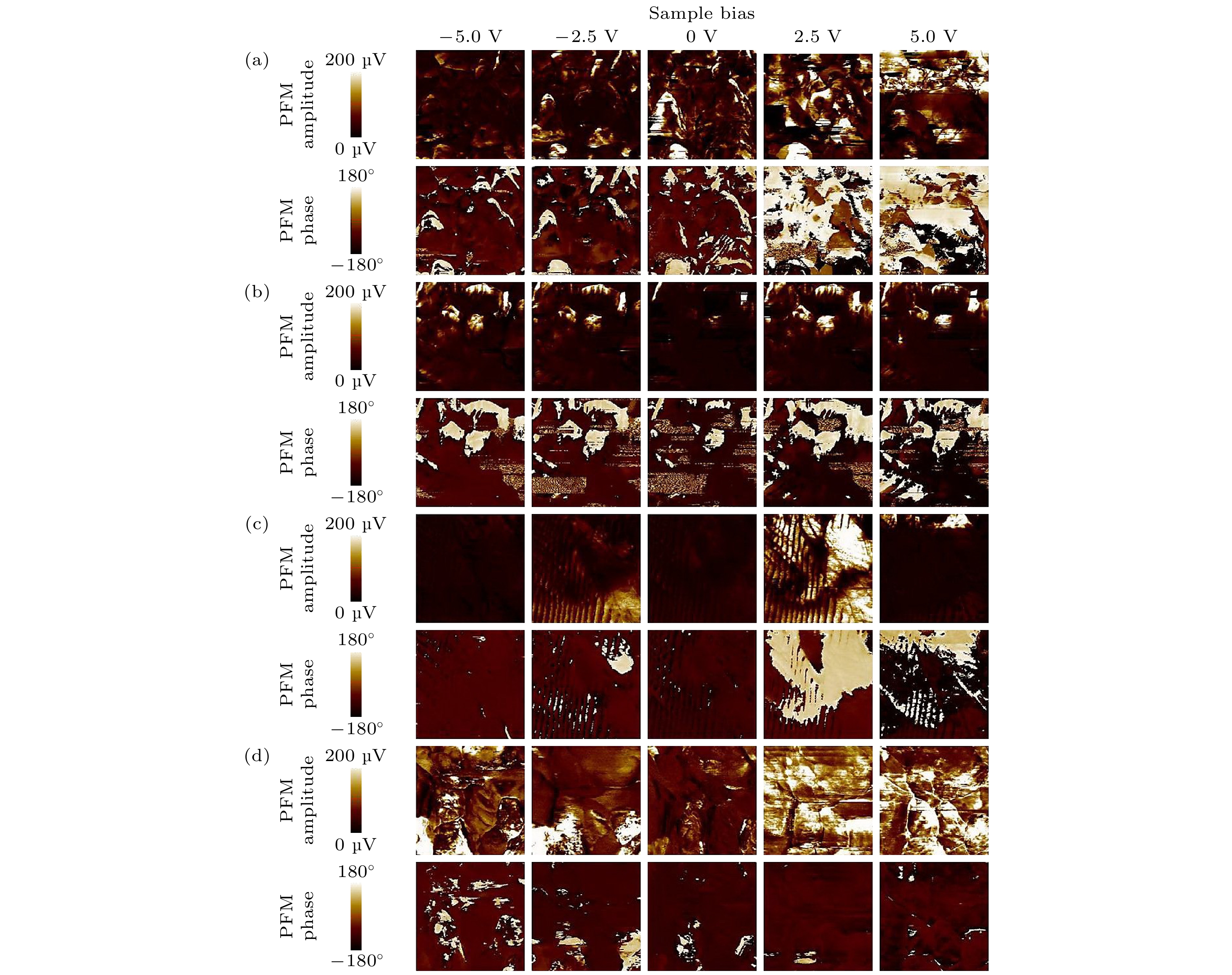
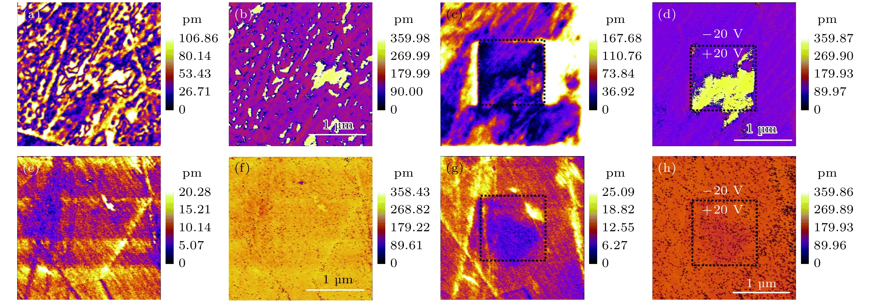
图 17 BF-BT-0.05 NT的垂直压电力显微镜(VPFM) (a)振幅和(b)相位图[103]; BF-BT-0.05 NT在±20 V极化后的(c)振幅和(d)相位[103]; BF-BT-0.12 NT的VPFM (e)振幅[103]和(f)相位图[103]; BF-BT-0.12 NT在±20 V极化后的(g)振幅和(h)相位图[103]
Fig. 17. (a) Amplitude and (b) phase images of vertical piezoelectric force microscopy (VPFM) for BF-BT-0.05 NT[103]; (c) amplitude and (d) phase images of PFM after poling with ±20 V voltage for BF-BT-0.05 NT[103]; (e) amplitude and (f) phase images of VPFM for BF-BT-0.12 NT[103]; (g) amplitude and (h) phase images of PFM after poling with ±20 V voltage for BF-BT-0.12 NT[103].
图 18 (a) 样本结构和弯曲样品的示意图(弯曲半径R); (b) 不同拉伸应变的P(VDF-TrFE)薄膜PFM相位图[106]; (c) 不同振幅和不同持续时间的脉冲电压下, 不同拉伸应变的P(VDF-TrFE)薄膜的PFM相位图[106]
Fig. 18. (a) Sample structure and schematic drawings of the flat and bent sample; (b) PFM phase images of a ferroelectric P(VDF-TrFE) film with different tensile strains[106]; (c) under the condition of voltage pulses of different amplitudes and different durations, PFM phase images of a P(VDF-TrFE) film with different tensile strains[106].
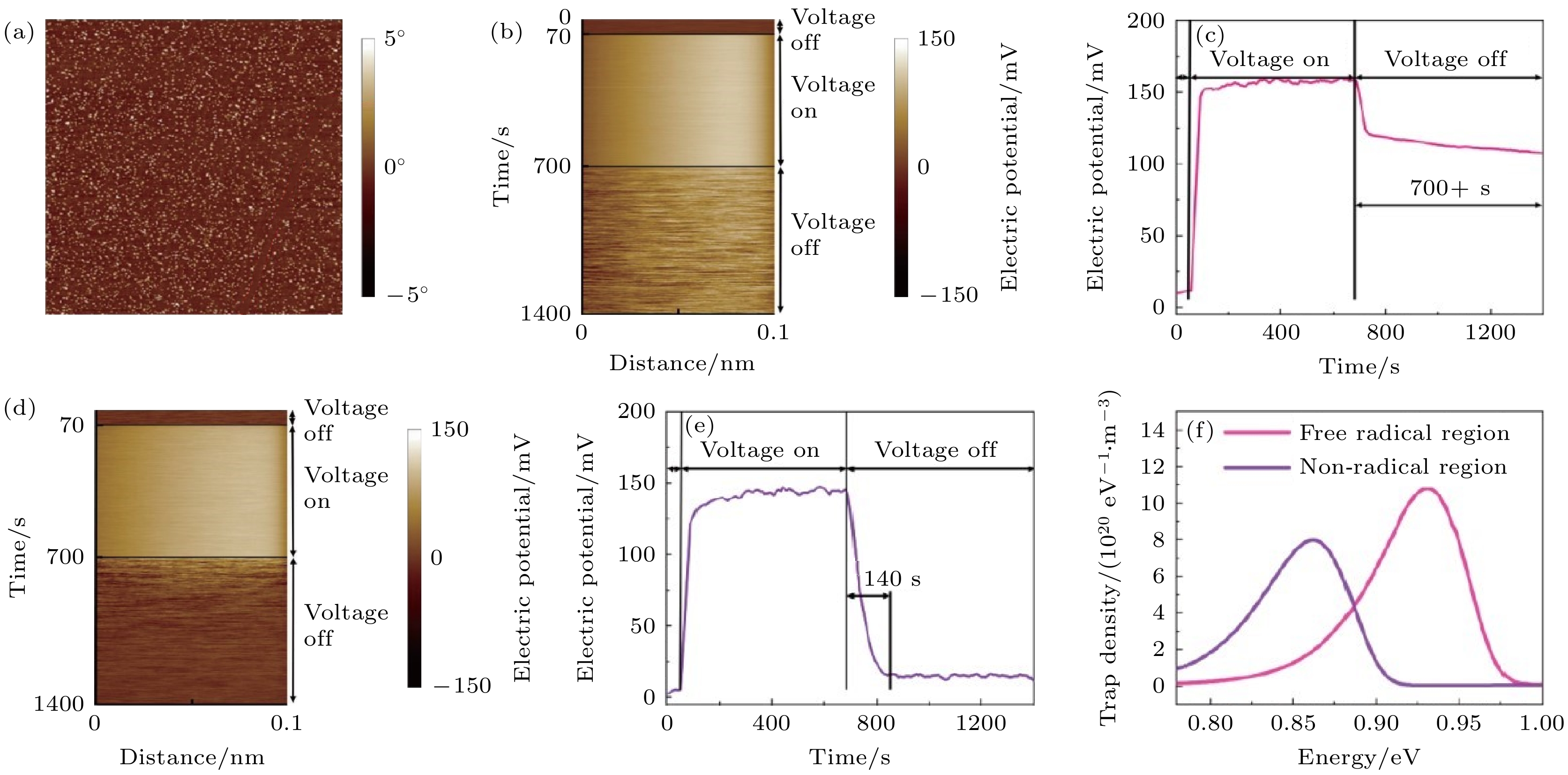
图 19 (a) EP表面的MFM图(扫描区域5 μm×5 μm)[113]; (b), (c) KPFM图和自由基区电势分布[113]; (d), (e) KPFM图和非自由基区电势分布; (f) 自由基区和非自由基区的深陷参数[113]
Fig. 19. (a) MFM map of the EP surface[113]; (b), (c) KPFM map and value of the potential in the radical region[113]; (d), (e) KPFM map and value of the potential in the non-radical region[113]; (f) deep trap parameters in the radical and non-radical regions[113].
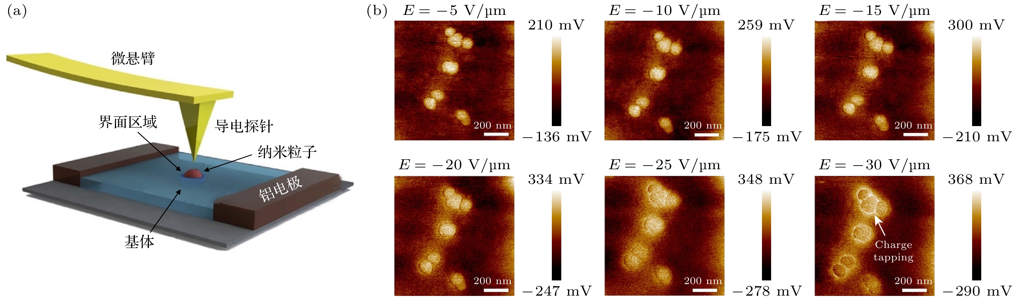
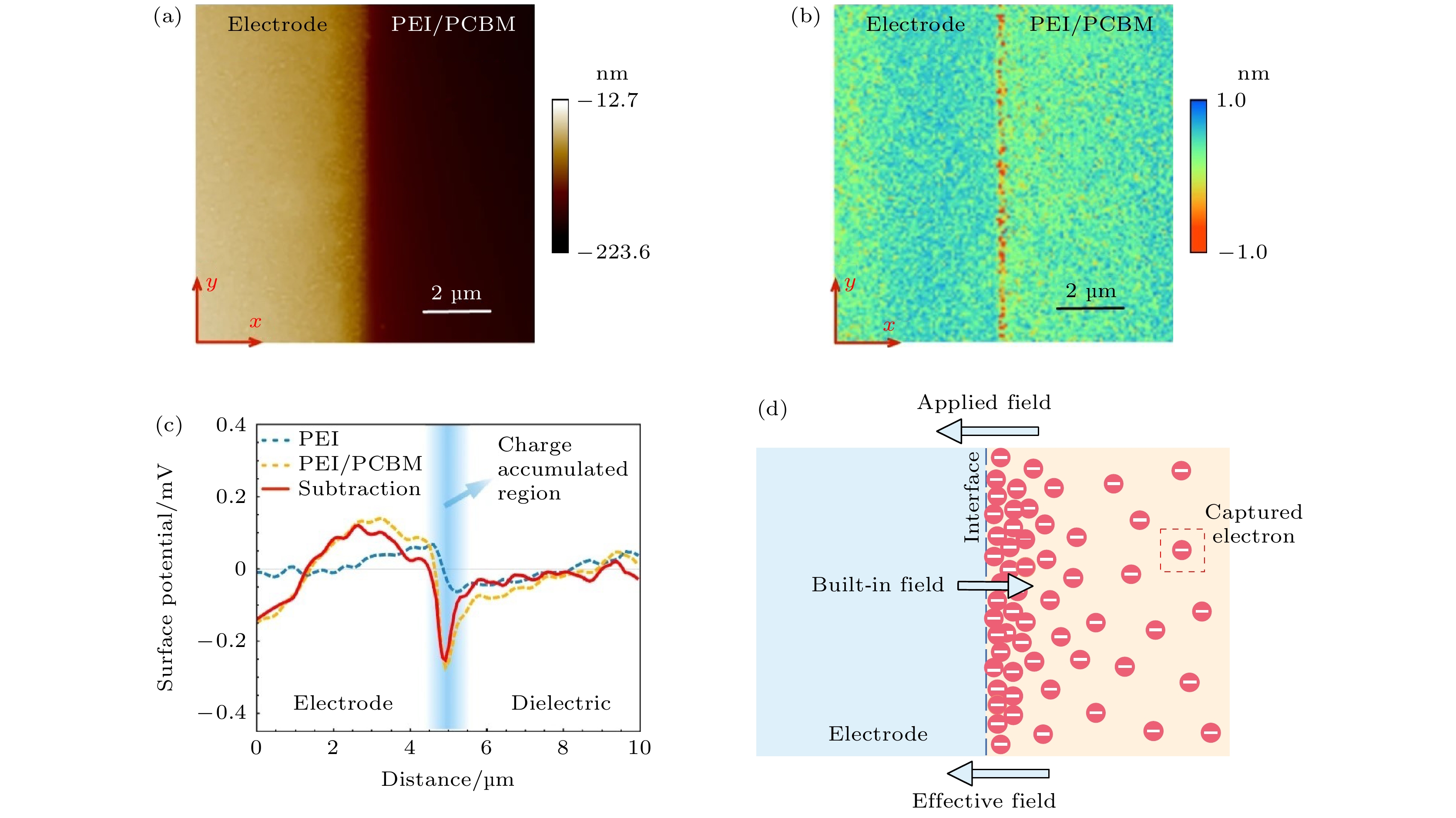
图 21 KPFM 测试示意图 (a), (b) PEI/PCBM 复合材料的(a)形貌和(b)表面电位映射[118]; (c) 沿水平轴的表面电位分布图[118]; (d) 分子半导体捕获电子形成的内建电场示意图[118]
Fig. 21. Schematic diagram of the KPFM testing: (a) Topography and (b) surface potential mapping of the PEI/PCBM composite[118]; (c) surface potential profiles along the horizontal axis derived from the surface potential mappings[118]; (d) schematic illustration of the built-in electric field formed by the molecular semiconductor captured electrons[118].
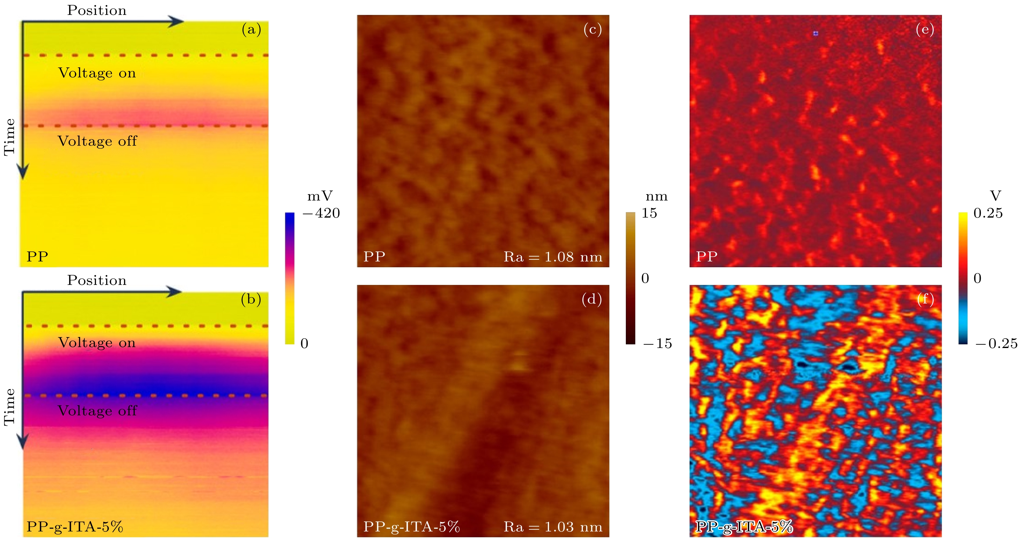
图 22 PP和PP-g-ITA的(a), (b)表面电位随时间变化的KPFM图[119]; (c), (d) AFM-IR形貌图[119]; (e), (f) 1780 cm–1红外激光下AFM-IR化学谱图[119]
Fig. 22. (a), (b) Time-dependent surface potential distribution on the scanned line in pristine PP and PP-g-ITA of KPFM[119]; (c), (d) AFM-IR topography of the specimens surface for pristine PP and the PP-g-ITA[119]; (e), (f) AFM-IR chemical map irradiated with a 1780 cm–1 laser[119].
表 1 功能化原子力显微镜简介
Table 1. Introduction to functional atomic force microscopy.
分类 名称 功能 应用 表征材料
电学性能静电力显微镜[15] 运用导电悬臂探测样品表面铁电区域, 得到纳米尺度的区域电学性能图. 样品表面电势[21]
检测相间结构[22]
研究电荷传播[23]
检测电荷分布[24]
电荷存储[25]导电原子力显微镜[26] 使用导电的偏压探针接触式扫描样品表面, 测量样品导电性. 测量局域电导率[27]
测量电流-电压曲线[28]
绘制能带分布[29]
研究纳米级电阻开关[28]开尔文探针力显微镜[16] 在非接触模式下通过检测探针与样品之间的静电信号提供样品表面电势等相关信息. 测量探针尖端和样品表面电位差[30]
测量空间电荷分布[31]
评估缺陷状态[32]压电响应力显微镜[33] 在接触模式下基于逆压电效应原理测量样品的局域压电响应能力. 研究铁电畴[34]
记录纳米级磁滞回线[35]
检测电致收缩/膨胀[36]
观察拓扑状态[37]扫描电容显微镜[38] 记录样品和金属探针之间的局部电容变化. 测量局部电容[39]
测量载流子浓度分布[40]
局部电荷的捕捉/释放[41]表征材料
化学结构原子力显微镜-红外光谱[20] 使用AFM探针的端检测样品特定区域中由于吸收红外辐射而导致的热膨胀, 来获得样品的红外吸收光谱及化学成分分布图谱. 纳米级红外光谱[42]
化学成分分布[43]
材料组分逆向分析[43]
纳米结晶度变化[44]
纤维中的分子取向[45]拉曼光谱-原子力显微镜[46] 使用激发激光来检测样品表面光学信号, 提供局部拉曼光谱, 表征样品表面的局部化学组成. 分析化学成分[47]
分析化学构象
获取形貌信息[48]
测量黏弹性[49]表征材料
力学性能力调制显微镜[50] 计算样品表面硬度、黏弹性等力学性能. 测量存储模量和损耗模量[51]
测量局部杨氏模量[52]
测量表面弹性变化[53]横向力显微镜[54] 通过检测悬臂在扫描样品时的扭曲来检测样品的摩擦力、黏附力等力学性能. 测量微区摩擦性能[55]
测量样品刚度[56]
测量表面黏附力
测量拓扑特性[57] 下载: 导出CSV
-
[1] Lewis T J 1994 IEEE Trans. Dielectr. Electr. Insul. 1 812
Google Scholar
[2] Frechette M F, Trudeau M L, Alamdar H, Boily S 2004 IEEE Trans. Dielectr. Electr. Insul. 11 808
Google Scholar
[3] Nelson J K, Fothergill J C, Dissado L A, Peasgood W 2002 Annual Report Conference on Electrical Insulation and Dielectric Phenomena Cancun, Mexico, October 20–24 2002 p295
[4] Nelson J K, Fothergill J C 2004 Nanotechnology 15 586
Google Scholar
[5] 王娇, 刘少辉, 陈长青, 郝好山, 翟继卫 2020 物理学报 69 217702
Google Scholar
Wang J, Liu S H, Chen C Q, Hao H S, Zhai J W 2020 Acta Phys. Sin. 69 217702
Google Scholar
[6] Lau K Y, Vaughan A S, Chen G 2015 IEEE Electr. Insul. Mag. 31 45
Google Scholar
[7] Wang B K, Barbiero M, Zhang Q M, Gu M 2019 Front. Inform. Tech. El. 20 608
Google Scholar
[8] Sun C, Müller E, Meffert M, Gerthsen D 2018 Microsc. Microanal. 24 99
Google Scholar
[9] Binnig G, Quate C F, Gerber C 1986 Phys. Rev. Lett. 56 930
Google Scholar
[10] Schmitz I, Schreiner M, Friedbacher G, Grasserbauer M 1997 Appl. Surf. Sci. 115 190
Google Scholar
[11] Binnig G, Rohrer H 1983 Surf, Sci. 126 236
[12] Martin Y, Williams C C, Wickramasinghe H K 1987 J. Appl. Phys. 61 4723
Google Scholar
[13] Zhong Q, Inniss D, Kjoller K, Elings V B 1993 Surf Sci. 290 L688
[14] Handschuh-Wang S, Wang T, Zhou X 2017 RSC Adv. 7 47464
Google Scholar
[15] Girard P 2001 Nanotechnology 12 485
Google Scholar
[16] Nonnenmacher M, Oboyle M P, Wickramasinghe H K 1991 Appl. Phys. Lett. 58 2921
Google Scholar
[17] Güthner P, Dransfeld K 1992 Appl. Phys. Lett. 61 1137
Google Scholar
[18] Gruverman A 1996 J. Vac. Sci. Technol. B. 14 602
Google Scholar
[19] Kalinin S V, Rodriguez B J, Jesse S, Karapetian E, Mirman B, Eliseev E A, Morozovska A N 2007 Annu. Rev. Mater. Res. 37 189
Google Scholar
[20] Dazzi A, Prater C B 2017 Chem. Rev. 117 5146
Google Scholar
[21] Singh A, Guha P, Panwar A K, Tyagi P K 2017 Appl. Surf. Sci. 402 271
Google Scholar
[22] El Khoury D, Fedorenko V, Castellon J, Bechelany M, Laurentie J C, Balme S, Fréchette M, Ramonda M, Arinero R 2017 Scanning 2017 1
[23] Zhao W, Cui W, Xu S, Wang Y, Zhang K, Wang D, Cheong L Z, Besenbacher F, Shen C 2018 Ultramicroscopy 196 24
[24] Sharma A, Basu S, Gupta N 2020 IEEE Trans. Dielectr. Electr. Insul. 27 866
Google Scholar
[25] Jones J T, Bridger P M, Marsh O J, Mcgill T C 1999 Appl. Phys. Lett. 75 1326
[26] Kelley T W, Granstrom E, Frisbie C D 1999 Adv. Mater. 11 261
Google Scholar
[27] Rosenberger M R, Chuang H J, Phillips M, Oleshko V P, McCreary K M, Sivaram S V, Hellberg C S, Jonker B T 2020 ACS Nano 14 4550
Google Scholar
[28] Lanza M, Celano U, Miao F 2017 J. Electroceram. 39 94
Google Scholar
[29] Li R, Taniguchi T, Watanabe K, Xue J 2020 Rev. Sci. Instrum. 91 073702
Google Scholar
[30] Glatzel T, Gysin U, Meyer E 2022 Microscopy 71 i165
[31] Faliya K, Kliem H, Dias C J 2017 IEEE Trans. Dielectr. Electr. Insul. 24 1913
Google Scholar
[32] Iglesias V, Lanza M, Zhang K, Bayerl A, Porti M, Nafría M, Aymerich X, Benstetter G, Shen Z Y, Bersuker G 2011 Appl. Phys. Lett. 99 103510
Google Scholar
[33] Proksch R, Nanophase C F, Sciences M, Kalinin S https://afm.oxinst.cn/assets/uploads/products/asylum/documents/Piezoresponse-Force-Microscopy-PFM-AFM.pdf [2022-5-27]
[34] Döring J, Eng L M, Kehr S C 2016 J. Appl. Phys. 120 084103
Google Scholar
[35] Eng L M 1999 Nanotechnology 10 405
Google Scholar
[36] Kalinin S V, Rodriguez B J, Jesse S, Shin J, Baddorf A P, Gupta P, Jain H, Williams D B, Gruverman A 2006 Microsc. Microanal. 12 206
Google Scholar
[37] McQuaid R G, McGilly L J, Sharma P, Gruverman A, Gregg J M 2011 Nat Commun 2 404
Google Scholar
[38] Matey J R, Blanc J 1985 J. Appl. Phys. 57 1437
Google Scholar
[39] Lee D T, Pelz J P, Bhushan B 2006 Nanotechnology 17 1484
Google Scholar
[40] Szyszka A, Dawidowski W, Stafiniak A, Prażmowska J, Ściana B, Tłaczała M 2017 Cryst. Res. Technol. 52 1700019
Google Scholar
[41] Hong J W, Shin S M, Kang C J, Kuk Y, Park S I 1999 Appl. Phys. Lett. 75 1760
Google Scholar
[42] Lu F, Jin M, Belkin M A 2014 Nat. Photonics 8 307
Google Scholar
[43] Tang F, Bao P, Su Z 2016 Anal. Chem. 88 4926
Google Scholar
[44] Marcott C, Lo M, Kjoller K, Prater C, Noda I 2011 Appl. Spectrosc. 65 1145
Google Scholar
[45] Dazzi A, Prater C B, Hu Q, Chase D B, Rabolt J F, Marcott C 2012 Appl. Spectrosc. 66 1365
Google Scholar
[46] Fernandes J P C, Mareau V H, Gonon L 2017 Int. J. Polym. Anal. Charact. 23 113
[47] Surtchev M, Magonov S, Zayats S, Wall M https://assets.thermofisher.com/TFS-Assets/CAD/Application-Notes/AN52664-Characterization-Polymer-Blends-Raman-AFM-2015.pdf [2022-6-28]
[48] Schmidt U, Dieing T, Weishaupt K, Liu W, Yang J 2012 Microsc. Microanal. 18 1504
Google Scholar
[49] Schmidt U, Liu W, Yang J, Dieing T, Weishaupt K 2015 Microsc. Microanal. 21 2189
Google Scholar
[50] Troyon M, Wang Z, Pastre D, Lei H, Hazotte A 1997 Nanotechnology 8 163
Google Scholar
[51] Radmacher M, Tillmann R, Gaub H 1993 Biophys. J. 64 735
Google Scholar
[52] Price W J, Leigh S A, Hsu S M, Patten T E, Liu G Y 2006 J. Phys. Chem. A 110 1382
Google Scholar
[53] Maivald P, Butt H, Gould S, Prater C, Drake B, Gurley J, Elings V, Hansma P 1991 Nanotechnology 2 103
Google Scholar
[54] Schwarz U D, KoSter P, Wiesendanger R 1996 Rev. Sci. Instrum. 67 2560
Google Scholar
[55] Yamanaka K, Tomita E 2014 Jpn. J. Appl. Phys. 34 2879
Google Scholar
[56] Weymouth A J, Hofmann T, Giessibl F J 2014 Science 343 1120
Google Scholar
[57] Goddenhenrich T, Muller S, Heiden C 1994 Rev. Sci. Instrum. 65 2870
Google Scholar
[58] Chelakara Satyanarayana K, Bolton K 2012 Polymer 53 2927
Google Scholar
[59] Mohammadi B, Yousefi A A, Bellah S M 2007 Polym. Test. 26 42
Google Scholar
[60] Ye H J, Yang L, Shao W Z, Sun S B, Zhen L 2013 RSC Adv. 3 23730
Google Scholar
[61] Gil H A, Faria R M, Kawano Y 1998 Polym. Degrad. Stab. 61 265
Google Scholar
[62] Tiwari V K, Kulriya P K, Avasthi D K, Maiti P 2009 J. Phys. Chem. B 113 11632
Google Scholar
[63] Ye H J, Yang L, Shao W Z, Li Y, Sun S B, Zhen L 2014 RSC Adv. 4 13525
Google Scholar
[64] Wang M, Wang S, Hu J, Li H, Ren Z, Sun X, Wang H, Yan S 2020 Macromolecules 53 5971
Google Scholar
[65] Gregorio R 2006 J. Appl. Polym. Sci. 100 3272
Google Scholar
[66] Gregorio R, Capitao R 2000 J. Mater. Sci. 35 299
Google Scholar
[67] Li W, Meng Q, Zheng Y, Zhang Z, Xia W, Xu Z 2010 Appl. Phys. Lett. 96 334
[68] Lovinger A J 1980 Polymer 21 1317
Google Scholar
[69] Prest W M, Luca D J 1978 J. Appl. Phys. 49 5042
Google Scholar
[70] Ghosh S K, Rahman W, Middya T R, Sen S, Mandal D 2016 Nanotechnology 27 215401
Google Scholar
[71] Barrau S, Ferri A, Da Costa A, Defebvin J, Leroy S, Desfeux R, Lefebvre J M 2018 ACS Appl. Mater. Interfaces 10 13092
Google Scholar
[72] Thakur Y, Zhang T, Iacob C, Yang T, Bernholc J, Chen L Q, Runt J, Zhang Q M 2017 Nanoscale 9 10992
Google Scholar
[73] Dang Z M, Yuan J K, Yao S H, Liao R J 2013 Adv. Mater. 25 6334
Google Scholar
[74] Li H, Yang T, Zhou Y, Ai D, Yao B, Liu Y, Li L, Chen L Q, Wang Q 2020 Adv. Funct. Mater. 31 2006739
[75] Wang R, Xu H, Cheng S, Liang J, Gou B, Zhou J, Fu J, Xie C, He J, Li Q 2022 Energy Storage Mater. 49 339
Google Scholar
[76] Moharana S, Sai S, Mahaling R N 2018 J. Adv. Dielectr. 08 1850017
[77] 王娇, 刘少辉, 周梦, 郝好山, 翟继卫 2020 物理学报 69 218101
Google Scholar
Wang J, Liu S H, Zhou M, Hao H S, Zhai J W 2020 Acta Phys. Sin. 69 218101
Google Scholar
[78] Chen Z, Shen Z, Liu Y, Zhang Y, Yan S, Feng R, Zhao T, Zhao G, Xiong C, Dong L 2020 Energy Storage Mater. 33 1
Google Scholar
[79] Yin K, Zhou Z, Schuele D E, Wolak M, Zhu L, Baer E 2016 ACS Appl. Mater. Interfaces 8 13555
Google Scholar
[80] Ponting M, Hiltner A, Baer E 2010 Macromol. Symp. 294 19
Google Scholar
[81] Wolak M A, Wan A S, Shirk J S, Mackey M, Hiltner A, Baer E 2012 J. Appl. Polym. Sci. 123 2548
Google Scholar
[82] Tang S, Zhou Z, Mackey M, Carr J M, Mu R, Flandin L, Schuele D E, Baer E, Lei Z 2014 Polymer 55 8
Google Scholar
[83] Lewis T J 2005 J. Phys. D:Appl. Phys. 38 202
Google Scholar
[84] Tanaka T, Kozako M, Fuse N, Ohki Y 2005 IEEE Trans. Dielectr. Electr. Insul. 12 669
Google Scholar
[85] Kirkpatrick S 1973 Rev. Mod. Phys. 45 574
Google Scholar
[86] Takada T, Hayase Y, Tanaka 2008 IEEE Trans. Dielectr. Electr. Insul. 15 152
Google Scholar
[87] Peng S, Zeng Q, Yang X, Hu J, Qiu X, He J 2016 Sci Rep 6 38978
Google Scholar
[88] Zheng C, Zhang W, Zhao H, Wang X, Sun Z, Yang J 2014 IEEE Trans. Dielectr. Electr. Insul. 21 1493
Google Scholar
[89] Seiler J, Kindersberger J 2014 IEEE Trans. Dielectr. Electr. Insul. 21 537
Google Scholar
[90] Deschler J, Seiler J, Kindersberger J 2017 IEEE Trans. Dielectr. Electr. Insul. 24 1027
Google Scholar
[91] Raetzke S, Kindersberger J 2006 IEEJ Trans. Fundam. Mater. 126 1044
Google Scholar
[92] Raetzke S, Kindersberger J 2010 IEEE Trans. Dielectr. Electr. Insul. 17 607
Google Scholar
[93] Liu Y, Yang T, Zhang B, Williams T, Lin Y T, Li L, Zhou Y, Lu W, Kim S H, Chen L Q, Bernholc J, Wang Q 2020 Adv. Mater. 32 e2005431
Google Scholar
[94] Bi M, Hao Y, Zhang J, Lei M, Bi K 2017 Nanoscale 9 16386
Google Scholar
[95] Mao Y P, Mao S Y, Ye Z G, Xie Z X, Zheng L S 2010 J. Appl. Phys. 108 L515
[96] Peng S, Yang X, Wang S, Zhou Y, Hu J 2019 Adv. Mater. 31 1807722
Google Scholar
[97] Xu K, Sun W, Shao Y, Wei F, Zhang X, Wang W, Li P 2018 Nanotechnol. Rev. 7 605
Google Scholar
[98] Altgilbers L L, Baird J, Freeman B L, Lynch C S, Shkuratov S I 1997 Ferroelectric Materials and Their Properties (Netherlands: Elsevier Science Publishers B.V.) pp329–359
[99] Ursic H, Prah U 2019 Proc. Math. Phys. Eng. Sci. 475 20180782
[100] Nonkumwong J, Ananta S, Srisombat L 2015 Appl. Phys. A 119 891
Google Scholar
[101] Nonkumwong J, Sriboriboon P, Kundhikanjana W, Srisombat L, Ananta S 2018 Integr. Ferroelectr. 187 210
Google Scholar
[102] Kholkin A, Bdikin I, Shvartsman V, Orlova A, Kiselev D, Bogomolov A, Kim S H 2004 MRS Online Proceedings Library 838 205
Google Scholar
[103] Zhu L F, Song A, Zhang B P, Gao X Q, Shan Z H, Zhao G L, Yuan J, Deng D, Shu H, Li J F 2022 J. Mater. Chem. A 10 7382
Google Scholar
[104] Furukawa T 1989 Phase Transit. 18 143
Google Scholar
[105] Ling Q D, Liaw D J, Zhu C, Chan D S H, Kang E T, Neoh K G 2008 Prog. Polym. Sci. 33 917
Google Scholar
[106] Cai R, Nysten B, Hu Z, Jonas A M 2017 Appl. Phys. Lett. 110 202901
Google Scholar
[107] Haque M A, Saif M T 2004 J Microelectromech. Syst. 101 6335
[108] Xiao Z, Poddar S, Ducharme S, Hong X 2013 Appl. Phys. Lett. 103 112903
Google Scholar
[109] Zhang B, Wang Q, Zhang Y, Gao W, Hou Y, Zhang G 2019 Nanoscale 11 18046
Google Scholar
[110] Tao S, Yang W, Cheng Z, Zheng N, Ping Y, Schamiloglu E 2014 Appl. Phys. Lett. 105 082903
Google Scholar
[111] Wang T Y, Zhang B Y, Li D Y, Hou Y C, Zhang G X 2020 Nanotechnology 31 324001
Google Scholar
[112] Xie Q, Liang S, Fu K, Liu L, Huang H, Lü F 2018 IEEE Trans. Dielectr. Electr. Insul. 25 2157
Google Scholar
[113] Wang T, Li X, Zhang B, Li D, Liu J, Zhang G 2022 Sci. China Mater. 65 2884
Google Scholar
[114] Pourrahimi A M, Hoang T A, Liu D, Pallon L K, Gubanski S, Olsson R T, Gedde U W, Hedenqvist M S 2016 Adv. Mater. 28 8651
Google Scholar
[115] Peng S, Luo Z, Wang S, Liang J, Yuan C, Yuan Z, Hu J, He J, Li Q 2020 ACS Appl Mater Interfaces 12 53425
Google Scholar
[116] Watson J, Castro G 2015 J. Mater. Sci. :Mater. Electron. 26 9226
Google Scholar
[117] Zhang T, Chen X, Thakur Y, Lu B, Zhang Q, Runt J, Zhang Q 2020 Sci. Adv. 6 eaax6622
Google Scholar
[118] Yuan C, Zhou Y, Zhu Y, Liang J, Wang S, Peng S, Li Y, Cheng S, Yang M, Hu J, Zhang B, Zeng R, He J, Li Q 2020 Nat Commun 11 3919
Google Scholar
[119] Yuan C, Zhou Y, Zhu Y, Hu S, Liang J, Luo Z, Gao B, Zeng T, Zhang Y, Li J 2022 ACS Sustainable Chem. Eng. 10 8685
Google Scholar


 下载:
下载:
计量
- 文章访问数: 10040
- PDF下载量: 174
- 被引次数: 0
