


-
肖特基二极管是2.45 G弱能量密度无线能量收集系统的核心器件, 其性能决定了系统整流效率的上限. 从材料设计角度出发, 利用晶向优化技术和Sn合金化技术, 提出并设计了一种大有效质量、大亲和能和高电子迁移率的Ge基复合半导体. 在此基础上, 进一步利用器件仿真工具, 设定合理的器件材料物理参数与几何结构参数, 实现了一种2.45 G弱能量微波无线输能用Ge基肖特基二极管. 基于该器件SPICE模型的ADS整流电路仿真表明: 与传统Ge肖特基二极管相比, 该新型Ge基肖特基二极管在输入能量为–10— –20 dBm的弱能量工作区域, 能量转换效率提升约10%. 本文技术方案及相关结论, 可为解决2.45 G弱能量密度无线能量收集系统整流效率低的问题提供有益的参考.With the development of modern communication technology, unlimited energy harvesting technology has become more and more popular. Among them, the weak energy density wireless energy harvesting technology has broken through the limitations in traditional transmission lines and can use the “waste” energy in the environment, which has become very popular. The Schottky diode is the core device of the 2.45 G weak energy density wireless energy harvesting system, and its performance determines the upper limit of the system's rectification efficiency. From the material design point of view, using crystal orientation optimization technology and Sn alloying technology, we propose and design a Ge-based compound semiconductor with large effective mass, large affinity, and high electron mobility. On this basis, the device simulation tool is further used to set reasonable device material physical parameters and geometric structure parameters, and a Ge-based Schottky diode for 2.45 G weak energy microwave wireless energy transmission is realized. The simulation of the ADS rectifier circuit based on the SPICE model of the device shows that comparing with the conventional Schottky diode, the turn-on voltage of the device is reduced by about 0.1 V, the zero-bias capacitance is reduced by 6 fF, and the reverse saturation current is also significantly increased. At the same time, the designed new Ge-based Schottky diode is used as the core rectifier device to simulate the rectifier circuit. The results show that the new-style Ge-based Schottky diode is in the weak energy working area with input energy in a range of –10 — –20 dBm. The energy conversion efficiency is increased by about 10%. The technical solutions and relevant conclusions of this article can provide a useful reference for solving the problem of low rectification efficiency of the 2.45 G weak energy density wireless energy harvesting system.
-
Keywords:
- weak energy wireless transmission /
- Schottky diode /
- germanium-tin /
- crystal orientation /
- rectification efficiency
[1] 李妤晨, 陈航宇, 宋建军 2020 物理学报 69 108401
 Google Scholar
Li Y C, Chen H Y, Song J J 2020 Acta Phys. Sin. 69 108401
Google Scholar
[2] De S C, Meneghini M, Caria A, Dogmus E, Zegaoui M, Medjdoub F, Kalinic B, Cesca T, Meneghesso G, Zanoni E 2018 Mater. Today 11 153
[3] Wan S P, Huang K 2018 IEEE Antennas Wirel. Propag. Lett. 17 538
[4] Chen Y S, Chiu C W 2018 Int. J. RF Microwave Comput. Aided Eng. 28 1
[5] Erkmen F, Almoneef T S, Ramahi O M 2018 IEEE Trans. Microwave Theory Tech. 66 2433
Google Scholar
[6] Wonwoo L, Yonghee J 2018 Micromachines. 10 12
Google Scholar
[7] Song C Y, Huang Y, Zhou J F, Zhang J W, Yuan S, Carter P 2015 IEEE Trans. Antennas Propag. 63 3486
Google Scholar
[8] Hemour S, Zhao Y P, Lorenz C H P, Houssameddine D, Gui Y S, Hu C M, Wu K 2014 IEEE Trans. Microwave Theory Tech. 62 965
Google Scholar
[9] Abdelmalek B, Fedoua D, Ilyas B 2019 Wirel. Netw. 25 3029
Google Scholar
[10] Zheng S Y, Liu W J, Pan Y M 2019 IEEE Trans. Ind. Inf. 15 3334
Google Scholar
[11] Cansiz M, Altinel D, Kurt G K 2019 Energy Technol. 174 292
[12] Liu W F, Wang Y Y, Song J J 2020 Superlattices Microstruct. 28 106639
[13] 施敏, 伍国珏 著 (耿莉, 张瑞智 译) 2007 半导体器件物理 (北京: 西安交通大学出版社) 第 110−113页
Sze S M, Kwok K N (translated by Geng L, Zhang R Z) 2007 Physics of Semiconductor Devices (Xi’an: Xi’an jiaotong University Press) pp130−142 (in Chinese)
[14] Yang W, Song J J, Hu H Y, Zhang H M 2018 J. Nanoelectron. Optoelectron. 13 986
Google Scholar
[15] 杨雯, 宋建军, 任远, 张鹤鸣 2018 物理学报 67 198502
Google Scholar
Yang W, Song J J, Ren Y, Zhang H M 2018 Acta Phys. Sin. 67 198502
Google Scholar
[16] Yang W, Song J J, Miao Y H, Zhang J, Dai X Y 2019 Sci. Technol. Adv. Mater. 11 1315
[17] Zhai X, Song J J, Dai X Y 2019 IEEE Access 7 127438
Google Scholar
[18] Wirths S, Geiger R, Driesch V D N, Mussler G, Stoica T, Mantl S, Ikonic Z, Luysberg M, Chiussi S, Hartmann J M, Sigg H, Faist J, Buca D, Grützmacher D 2015 Nat. Photonics 9 88
Google Scholar
[19] Zhai X, Song J J, Dai X Y, Zhao T L 2020 Semicond. Sci. Technol. 35 085026
Google Scholar
[20] Amato M, Bertocchi M, Ossicini S 2016 J. Phys. D: Appl. Phys. 119 085705
Google Scholar
[21] Minnie M, Rajeev K S, Charita M 2020 Mater. Today 28 1445
[22] Huang W Q, Cheng B W, Xue C L, Li C B 2014 Physica B 443 43
Google Scholar
-
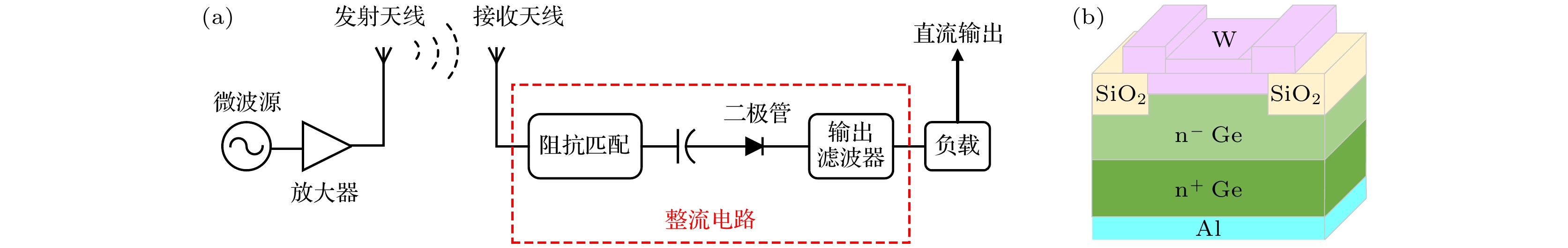
图 1 (a) 微波无线能量传输系统; (b) 典型肖特基二极管示意图
Fig. 1. (a) Microwave wireless energy transmission system; (b) schematic diagram of a typical Schottky diode.
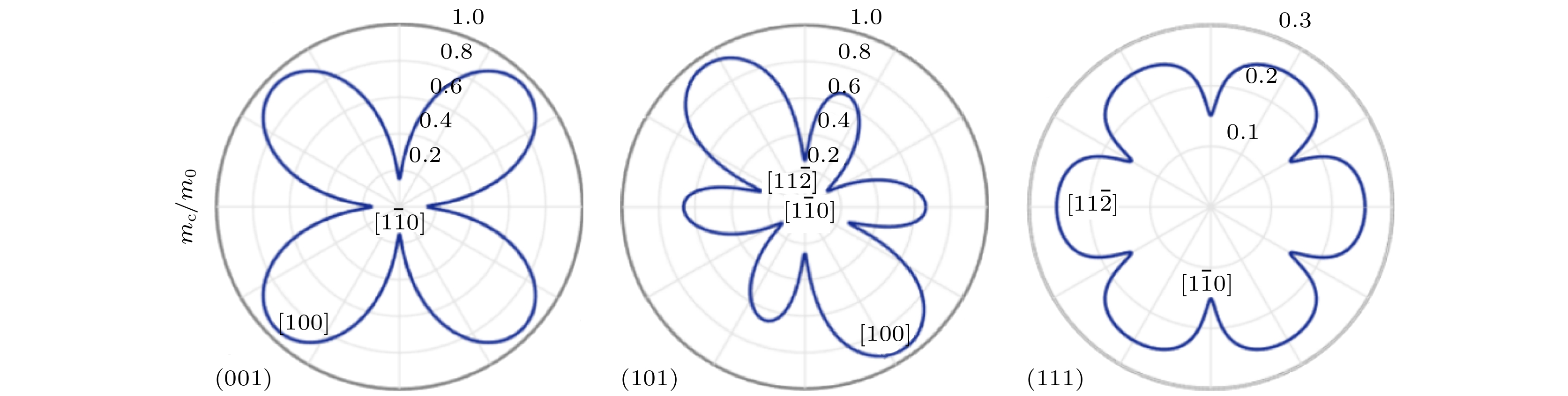
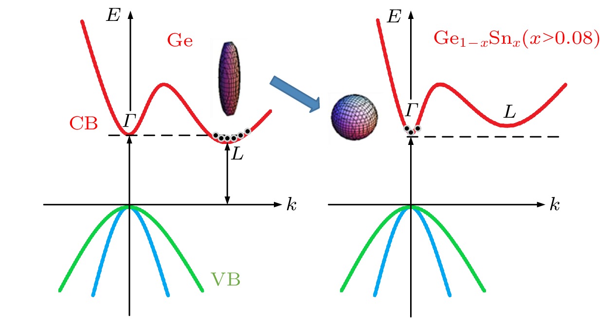
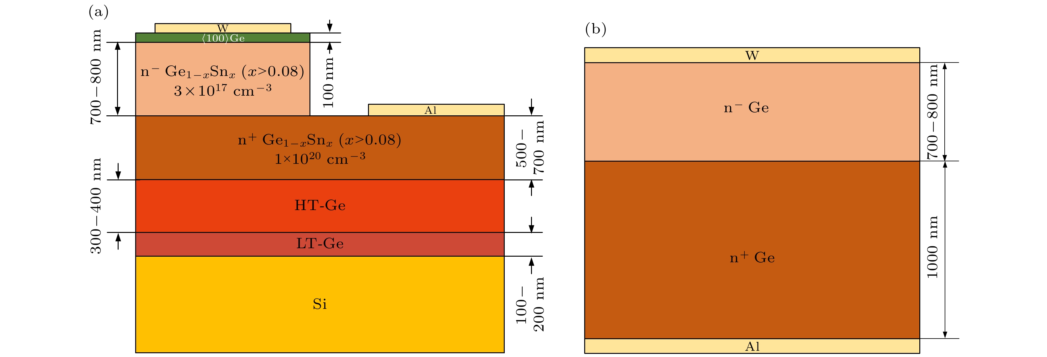
图 5 (a) 新型SBD器件剖面示意图含层结构材料物理参数和几何结构参数; (b)传统SBD
Fig. 5. (a) The cross-sectional schematic diagram of the new SBD device contains the physical parameters and geometric structure parameters of the layered structure material; (b) the traditional SBD.
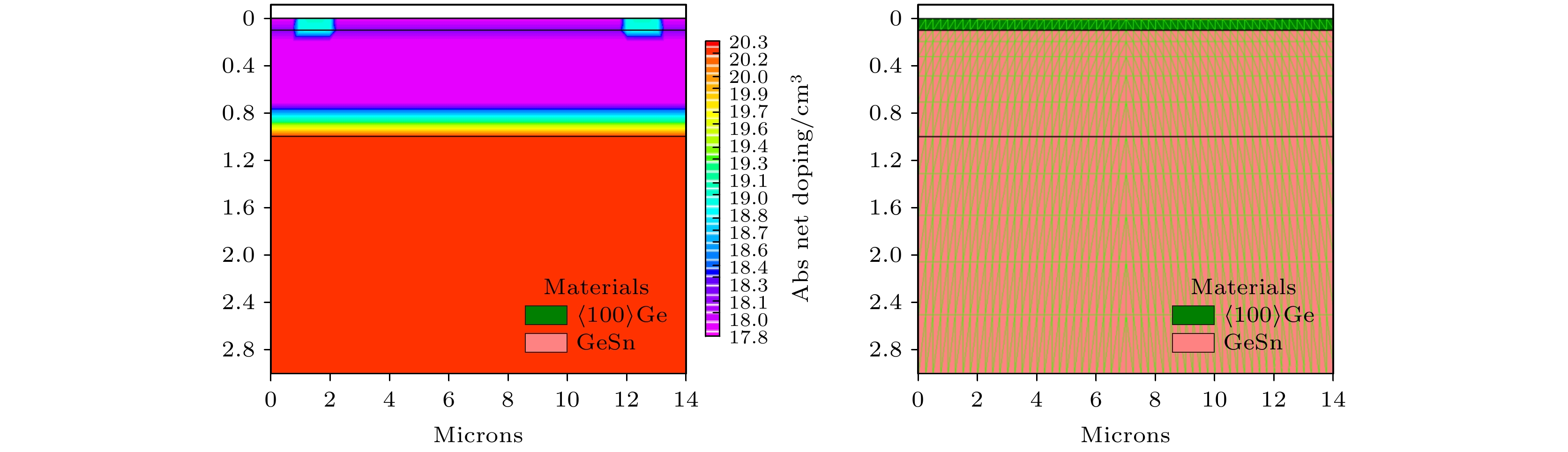
图 6 新型SBD器件Silvaco仿真结构和网格设置截图
Fig. 6. A screenshot of the Silvaco simulation structure and grid settings of the new SBD device.

图 7 不同厚度
$\left\langle {100} \right\rangle $ 晶向Ge帽层新型SBD器件正向伏安特性曲线Fig. 7. Forward V-J characteristic curve of new SBD device with different thickness
$\left\langle {100} \right\rangle $ crystal orientation Ge cap layer.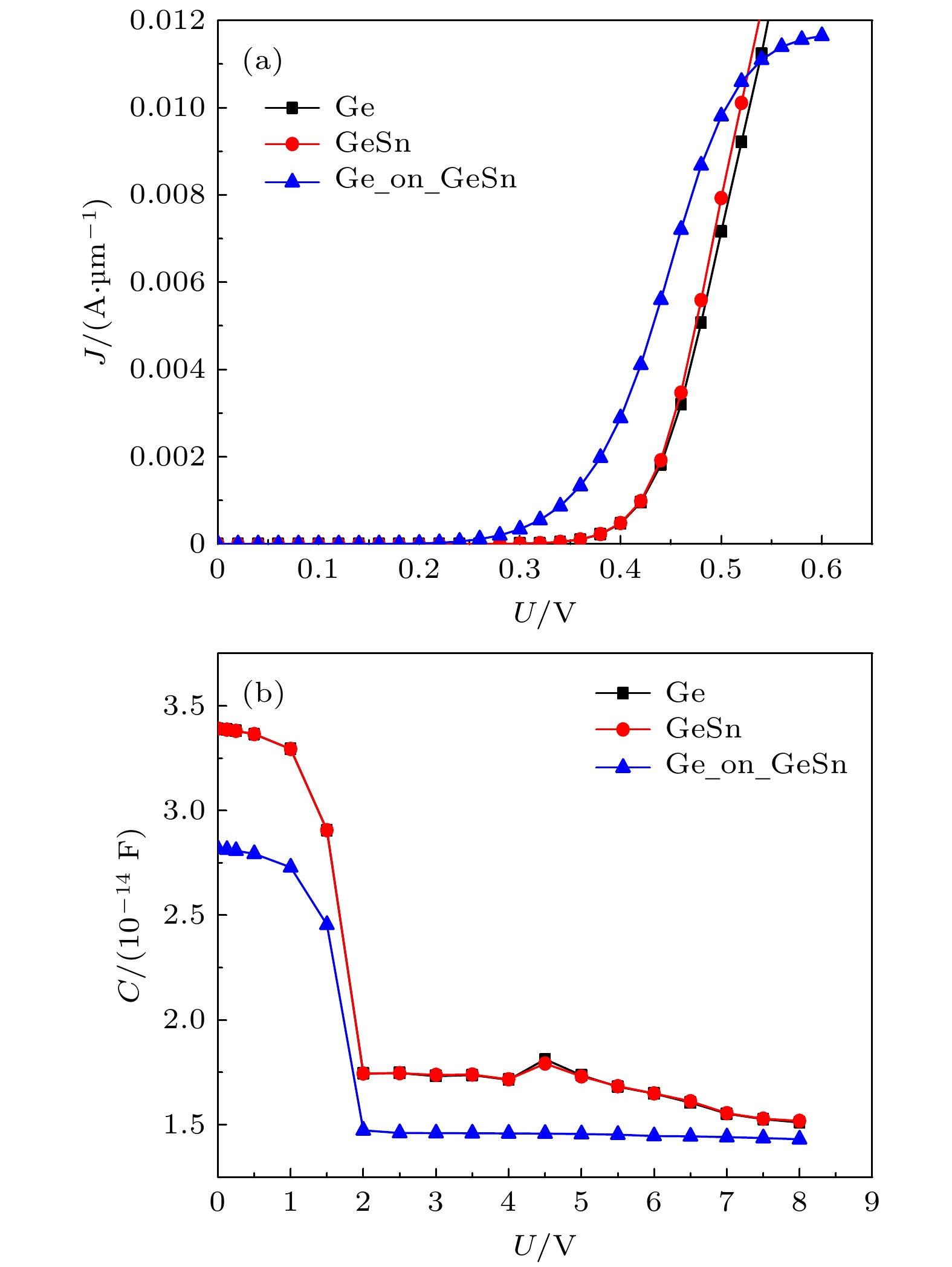
图 8 三种Ge基SBD器件伏安特性、电容特性仿真结果
Fig. 8. volt-ampere characteristic Capacitance-voltage characteristic simulation results of three Ge-based SBD devices.
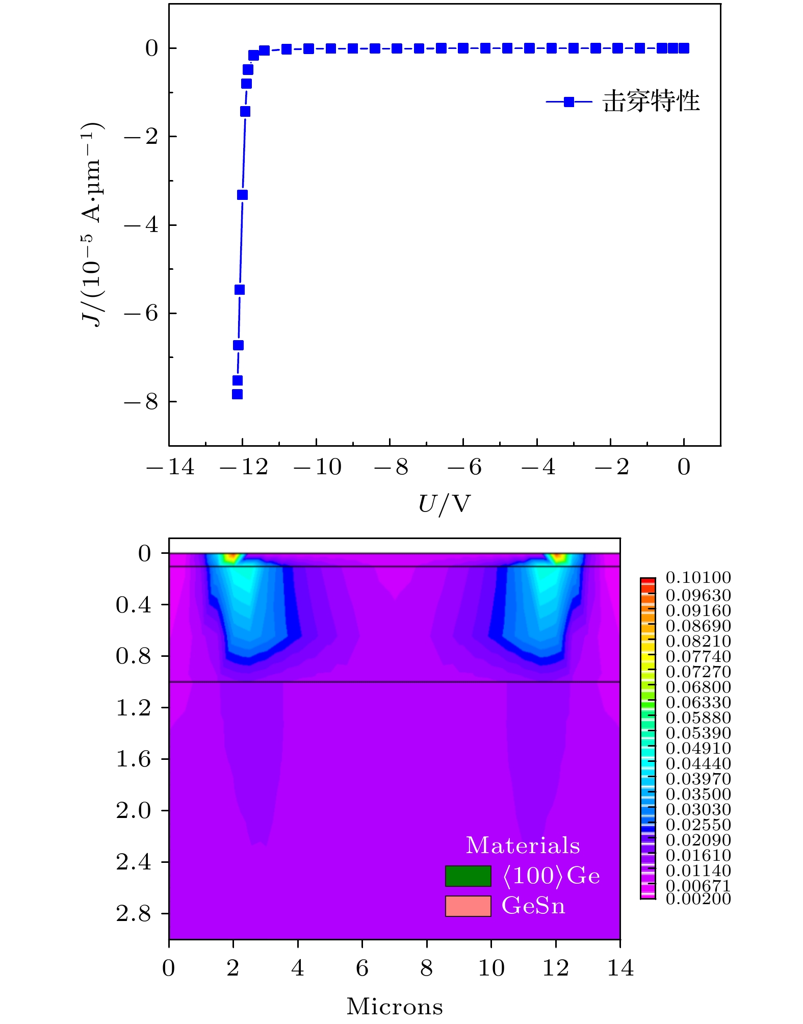
图 9 新型Ge基SBD器件击穿特性仿真结果
Fig. 9. Simulation results of the breakdown characteristics of the new Ge-based SBD device.
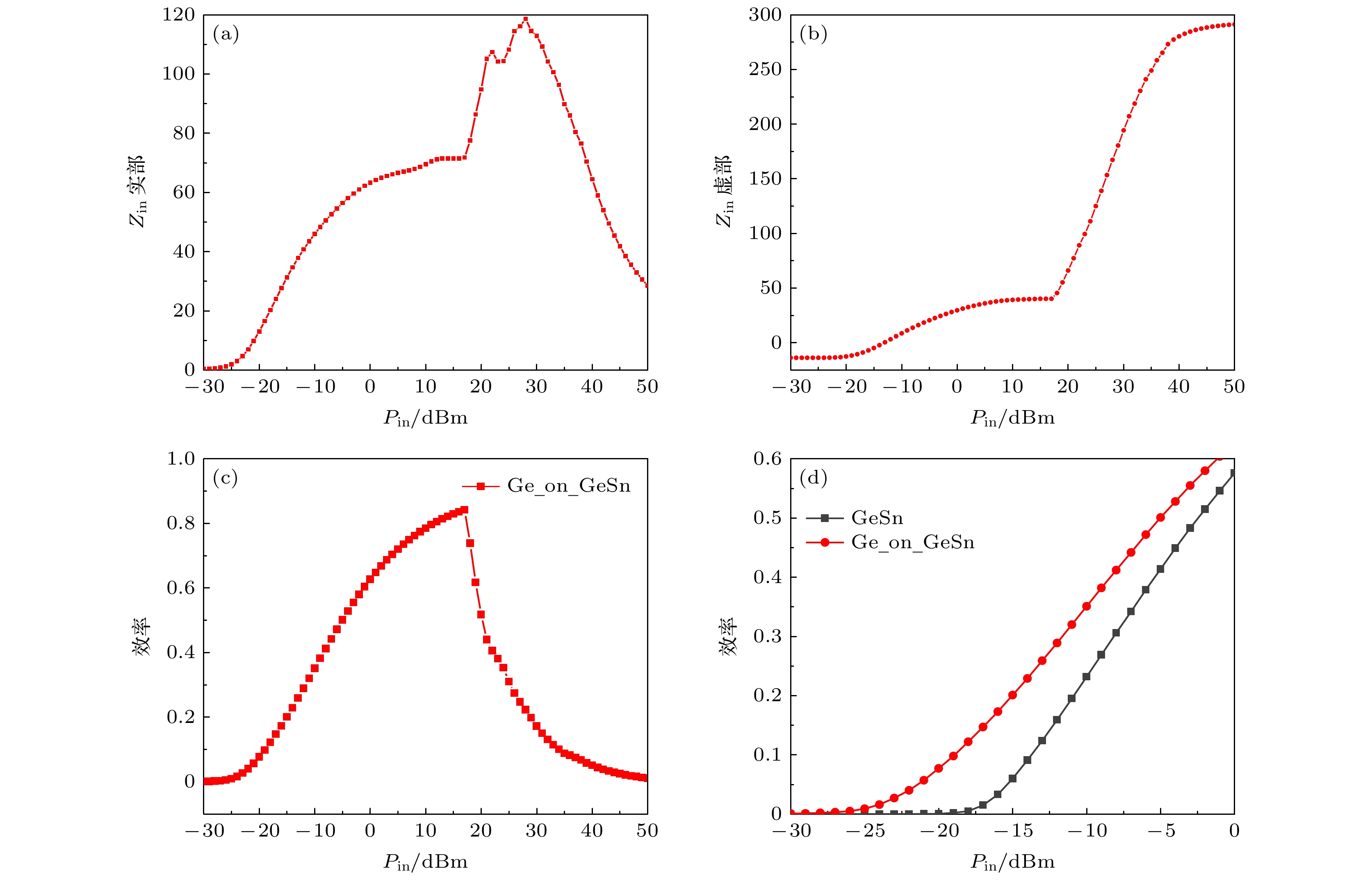
图 11 整流电路的仿真结果, 输入能量与 (a)阻抗实部、(b)阻抗虚部、(c)整流效率以及(d)弱能量区域整流效率的关系
Fig. 11. Simulation results of the rectifier circuit, the relationship between the input energy and (a) the real part of the impedance (b) the imaginary part of the impedance (c) the rectification efficiency (d) the rectification efficiency in the weak energy region.
表 1 三种Ge基SBD器件SPICE参数表
Table 1. SPICE parameter table of three Ge-based SBD devices.
参数 $ {B}_{v}/ $V $ {C}_{j0} $/fF $ {E}_{\rm{G}} $/eV $ {I}_{\rm{S}} $/A N $ {R}_{\rm{S}} $/${\Omega }$ M Ge 18.9 36 0.69 9.6235 × 10⁻¹¹ 0.999 2.9 0.5072 GeSn 19 36.2 0.69 9.628 × 10⁻¹¹ 0.999 2.8 0.5073 Ge_on_GeSn 11.4 30 0.69 1.0437 × 10⁻⁸ 1.106 11.6 0.4037  下载: 导出CSV
-
[1] 李妤晨, 陈航宇, 宋建军 2020 物理学报 69 108401
Google Scholar
Li Y C, Chen H Y, Song J J 2020 Acta Phys. Sin. 69 108401
Google Scholar
[2] De S C, Meneghini M, Caria A, Dogmus E, Zegaoui M, Medjdoub F, Kalinic B, Cesca T, Meneghesso G, Zanoni E 2018 Mater. Today 11 153
[3] Wan S P, Huang K 2018 IEEE Antennas Wirel. Propag. Lett. 17 538
[4] Chen Y S, Chiu C W 2018 Int. J. RF Microwave Comput. Aided Eng. 28 1
[5] Erkmen F, Almoneef T S, Ramahi O M 2018 IEEE Trans. Microwave Theory Tech. 66 2433
Google Scholar
[6] Wonwoo L, Yonghee J 2018 Micromachines. 10 12
Google Scholar
[7] Song C Y, Huang Y, Zhou J F, Zhang J W, Yuan S, Carter P 2015 IEEE Trans. Antennas Propag. 63 3486
Google Scholar
[8] Hemour S, Zhao Y P, Lorenz C H P, Houssameddine D, Gui Y S, Hu C M, Wu K 2014 IEEE Trans. Microwave Theory Tech. 62 965
Google Scholar
[9] Abdelmalek B, Fedoua D, Ilyas B 2019 Wirel. Netw. 25 3029
Google Scholar
[10] Zheng S Y, Liu W J, Pan Y M 2019 IEEE Trans. Ind. Inf. 15 3334
Google Scholar
[11] Cansiz M, Altinel D, Kurt G K 2019 Energy Technol. 174 292
[12] Liu W F, Wang Y Y, Song J J 2020 Superlattices Microstruct. 28 106639
[13] 施敏, 伍国珏 著 (耿莉, 张瑞智 译) 2007 半导体器件物理 (北京: 西安交通大学出版社) 第 110−113页
Sze S M, Kwok K N (translated by Geng L, Zhang R Z) 2007 Physics of Semiconductor Devices (Xi’an: Xi’an jiaotong University Press) pp130−142 (in Chinese)
[14] Yang W, Song J J, Hu H Y, Zhang H M 2018 J. Nanoelectron. Optoelectron. 13 986
Google Scholar
[15] 杨雯, 宋建军, 任远, 张鹤鸣 2018 物理学报 67 198502
Google Scholar
Yang W, Song J J, Ren Y, Zhang H M 2018 Acta Phys. Sin. 67 198502
Google Scholar
[16] Yang W, Song J J, Miao Y H, Zhang J, Dai X Y 2019 Sci. Technol. Adv. Mater. 11 1315
[17] Zhai X, Song J J, Dai X Y 2019 IEEE Access 7 127438
Google Scholar
[18] Wirths S, Geiger R, Driesch V D N, Mussler G, Stoica T, Mantl S, Ikonic Z, Luysberg M, Chiussi S, Hartmann J M, Sigg H, Faist J, Buca D, Grützmacher D 2015 Nat. Photonics 9 88
Google Scholar
[19] Zhai X, Song J J, Dai X Y, Zhao T L 2020 Semicond. Sci. Technol. 35 085026
Google Scholar
[20] Amato M, Bertocchi M, Ossicini S 2016 J. Phys. D: Appl. Phys. 119 085705
Google Scholar
[21] Minnie M, Rajeev K S, Charita M 2020 Mater. Today 28 1445
[22] Huang W Q, Cheng B W, Xue C L, Li C B 2014 Physica B 443 43
Google Scholar

 下载:
下载:


计量
- 文章访问数: 5977
- PDF下载量: 65
- 被引次数: 0
