


-
As an important branch of metamaterial-based devices, metamaterial absorber (MA) has aroused great interest and made great progress in the past several years. By manipulating the magnetic resonance and the electric resonance simultaneously, the effective impedance of MA will match the free space impedance, thus resulting in a perfect absorption of incident waves. Due to the advantages of thin thickness, high efficiency and tunable property, MA has been widely concerned in energy-harvesting and electromagnetic stealth. Since the first demonstration of MA in 2008, many MAs have been extensively studied in different regions, such as microwave frequency, THz, infrared frequency and optical frequency. At the same time, the absorber has been extended from the single-band to the dual-band, triple-band, multiple-band and broadband. In recent years, the dual-band absorber has received significant attention and has been widely studied. So far, however, most of MAs are composed of a bottom continuous metallic layer, which prevents electromagnetic waves from penetrating and makes electromagnetic waves absorbed or reflected. In this paper, an ultrathin flexible transmission absorber with a total thickness of 0.288 mm is designed and fabricated, which can be conformally integrated on an object with a curved surface. The absorber consists of three layers of structure: the bottom is a one-dimensional grating type metal line, the middle is the medium layer, and the surface metal layer is composed of two different sizes metal lines in parallel. Simulation and experimental results show that the absorptions of TE wave are 97.5% and 96.0% respectively at the two frequency points of 5 GHz and 7 GHz. The transmission of the TM wave above 90% is maintained from 3 GHz to 6.5 GHz. We also simulate the spatial electric field distribution and magnetic field distribution at two resonant frequencies, and explain the electromagnetic absorption mechanism of the proposed structure for TE wave. Secondly, when the incident angle increases to 60 degrees, the performance of the absorber is substantially unaffected, exhibiting good wide-angle characteristics. In addition, through the analysis of structural parameters, two absorption peaks of the proposed absorber can be independently adjusted, resulting in a flexible design. In conclusion, we propose both theoretically and experimentally a polarization-controlled transmission-type dual-band metamaterial absorber that can absorb the TE waves and transmit the TM wave efficiently, which has important applications in the case requiring bidirectional communication.
-
Keywords:
- metamaterial absorber /
- ultrathin flexibility /
- dual-band absorption /
- efficient transmission
[1] Almoneef T S, Ramahi O M 2015 Appl. Phys. Lett. 106 153902
 Google Scholar
[2] Ishikawa A, Tanaka T 2015 Sci. Rep. 5 12570
Google Scholar
[3] Xie Y, Fan X, Chen Y, Wilson J, Simons R N, Xiao J 2017 Sci. Rep. 7 40490
Google Scholar
[4] Liu X, Tyler T, Starr T, Starr A F, Jokerst N M, Padilla W J 2011 Phys. Rev. Lett. 107 045901
Google Scholar
[5] Li W, Valentine J 2014 Nano Lett. 14 3510
Google Scholar
[6] 马晓亮, 李雄, 郭迎辉, 赵泽宇, 罗先刚 2017 物理学报 66 147802
Google Scholar
Ma X L, Li X, Guo Y H, Zhao Z Y, Luo X G 2017 Acta Phys. Sin. 66 147802
Google Scholar
[7] Landy N I, Sajuyigbe S, Mock J J, Smith D R, Padilla W J 2008 Phys. Rev. Lett. 100 207402
Google Scholar
[8] Khuyen B X, Tung B S, Yoo Y J, Kim Y J, Lam V D, Yang J, Lee Y 2016 Curr. Appl. Phys. 16 1009
Google Scholar
[9] Khuyen B X, Tung B S, Yoo Y J, Kim Y J, Kim K W, Chen L, Lam V D, Lee Y 2017 Sci. Rep. 7 45151
Google Scholar
[10] Ding F, Cui Y, Ge X, Jin Y, He S 2012 Appl. Phys. Lett. 100 103506
Google Scholar
[11] Zhang Y, Duan J, Zhang B, Zhang W, Wang W 2017 J. Alloys Compd. 705 262
Google Scholar
[12] Tao H, Bingham C M, Strikwerda A C, Pilon D, Shrekenhamer D, Landy N I, Fan K, Zhang X, Padilla W J, Averitt R D 2008 Phys. Rev. B 78 241103
Google Scholar
[13] Wang W, Wang K, Yang Z, Liu J 2017 J. Phys. D: Appl. Phys. 50 135108
Google Scholar
[14] 张玉萍, 李彤彤, 吕欢欢, 黄晓燕, 张会云 2015 物理学报 64 117801
Google Scholar
Zhang Y P, Li T T, Lü H H, Huang X Y, Zhang H Y 2015 Acta Phys. Sin. 64 117801
Google Scholar
[15] Chen J, Li J, Liu Q H 2017 IEEE Trans. Microwave Theory Tech. 65 3689
Google Scholar
[16] Chen J, Li J, Liu Q H 2017 IEEE Trans. Microwave Theory Tech. 65 1896
[17] Liu X, Starr T, Starr A F, Padilla W J 2010 Phys. Rev. Lett 104 207403
Google Scholar
[18] Hasan D, Pitchappa P, Wang J, Wang T, Yang B, Ho C P, Lee C 2017 ACS Photonics 4 302
Google Scholar
[19] Hao J, Wang J, Liu X, Padilla W J, Zhou L, Qiu M 2010 Appl. Phys. Lett 96 251104
Google Scholar
[20] Wang W, Qu Y, Du K, Bai S, Tian J, Pan M, Ye H, Qiu M, Li Q 2017 Appl. Phys. Lett 110 101101
Google Scholar
[21] Wen Q, Zhang H, Xie Y, Yang Q, Liu Y 2009 Appl. Phys. Lett. 95 241111
Google Scholar
[22] Xu H, Wang G, Qi M, Liang J, Gong J, Xu Z 2012 Phys. Rev. B 86 205104
Google Scholar
[23] Wang B, Wang G, Sang T, Wang L 2017 Sci. Rep 7 41373
Google Scholar
[24] Xie J, Zhu W, Rukhlenko I D, Xiao F, He C, Geng J, Liang X, Jin R, Premaratne M 2018 Opt. Express 26 5052
Google Scholar
[25] Ma Y, Chen Q, Grant J, Saha S C, Khalid A, Cumming D R S 2011 Opt. Lett 36 945
Google Scholar
[26] Chen K, Adato R, Altug H 2012 ACS Nano 6 7998
Google Scholar
[27] Tao H, Bingham C M, Pilon D, Fan K, Strikwerda A C, Shrekenhamer D, Padilla W J, Zhang X, Averitt R D 2010 J. Phys. D: Appl. Phys. 43 225102
Google Scholar
[28] Singh P K, Korolev K A, Afsar M N, Sonkusale S 2011 Appl. Phys. Lett. 99 264101
Google Scholar
[29] Feng R, Ding W Q, Liu L H, Chen L X, Qiu J, Chen G Q 2014 Opt. Express 22 A335
Google Scholar
[30] Liu X, Lan C, Li B, Zhao Q, Zhou J 2016 Sci. Rep. 6 28906
Google Scholar
[31] Tung B S, Khuyen B X, Kim Y J, Lam V D, Kim K W, Lee Y 2017 Sci. Rep. 7 11507
Google Scholar
[32] Yoo Y J, Kim Y J, Tuong P V, Rhee J Y, Kim K W, Jang W H, Kim Y H, Cheong H, Lee Y 2013 Opt. Express 21 32484
Google Scholar
[33] Yue W, Wang Z, Yang Y, Han J, Li J, Guo Z, Tan H, Zhang X 2016 Plasmonics 11 1557
Google Scholar
[34] Liu N, Mesch M, Weiss T, Hentschel M, Giessen H 2010 Nano Lett. 10 2342
Google Scholar
-
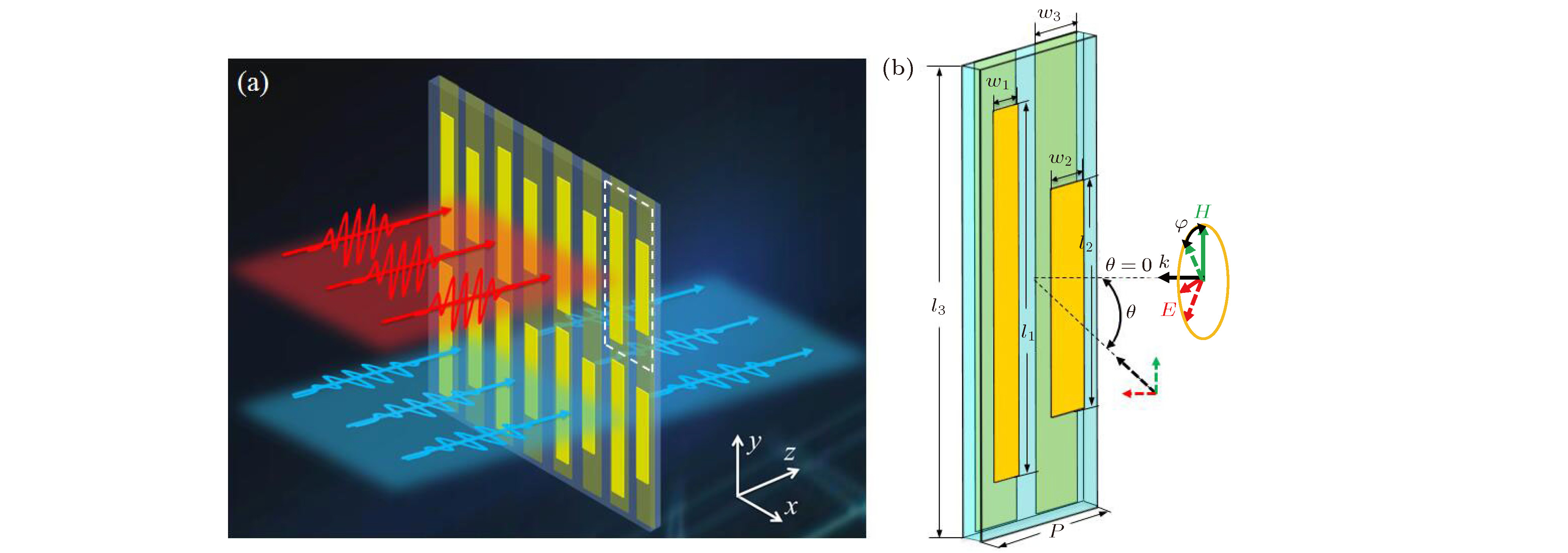
图 1 (a) 超薄柔性透射型双频吸收器的效果示意图; (b)基本单元结构示意图
Fig. 1. (a) Schematic demonstration of the proposed ultrathin flexible transmission dual-band absorber; (b) schematic diagram of the basic unit structure.
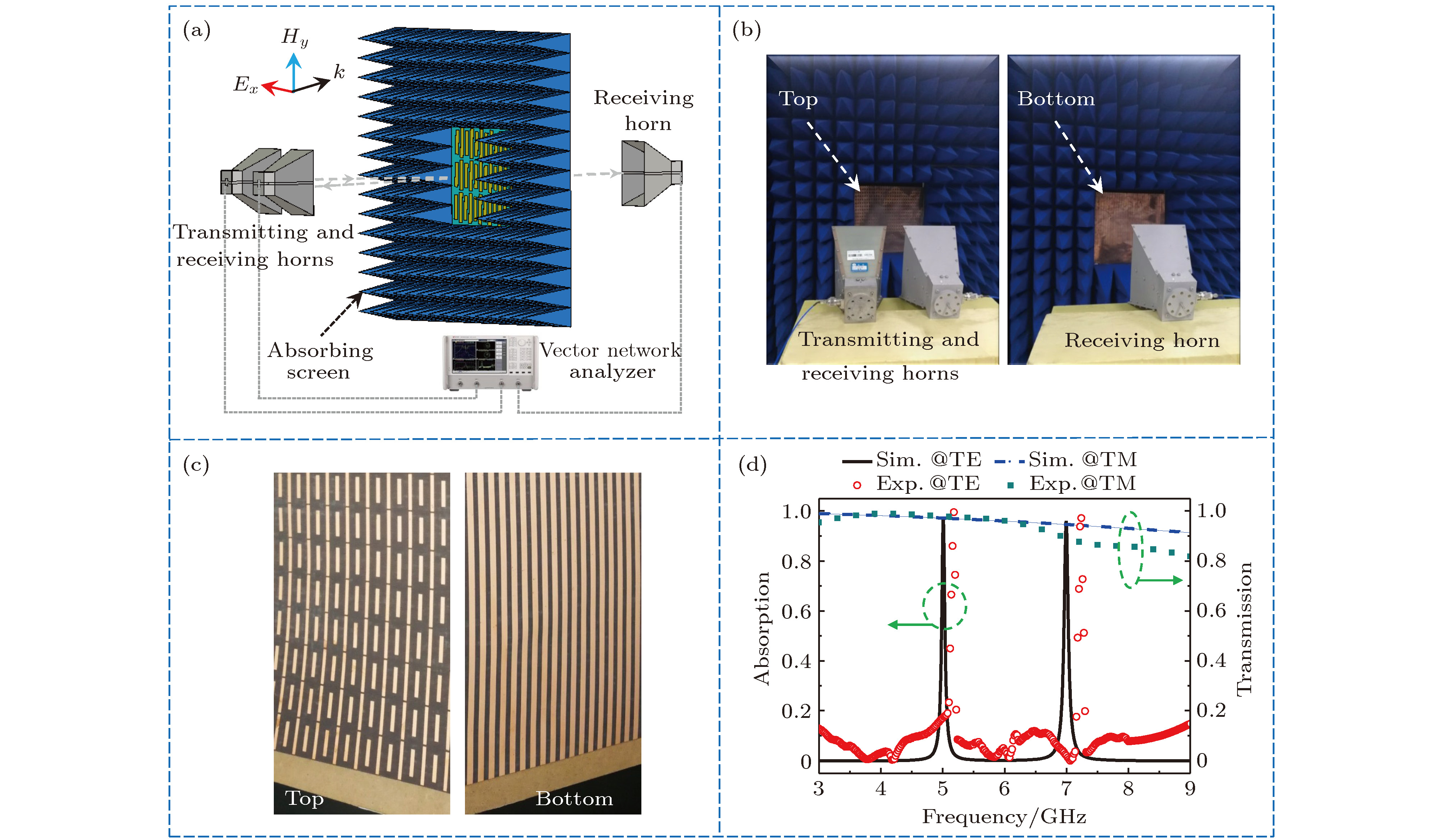
图 2 (a) 实验装置示意图; (b)测试环境照片; (c) 加工实物照片; (d)仿真和实验结果
Fig. 2. (a) Schematic demonstration of experimental setup; (b) photograph of experimental setup; (c) photograph of the fabricated sample; (d) simulated and measured results.
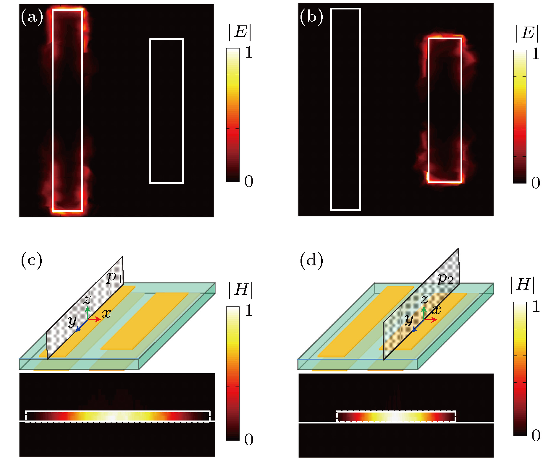
图 3 电场分布 (a) f = 5 GHz, (b) f = 7 GHz; 磁场分布 (c) f = 5 GHz, (d) f = 7 GHz
Fig. 3. The electric field distributions at (a) f = 5 GHz and (b) f = 7 GHz, respectively; the magnetic field distributions at (c) f = 5 GHz and (d) f = 7 GHz, respectively.
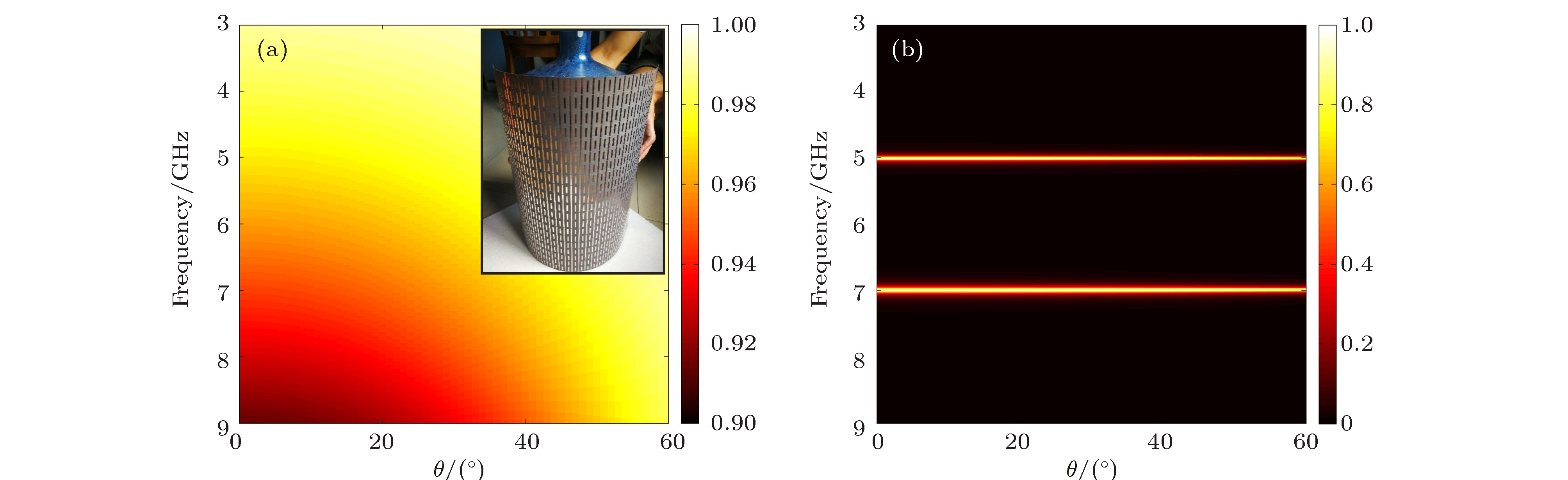
图 4 (a) TM波随入射角度变化的透射谱, 插图为弯曲的加工样品覆盖在圆柱形物体表面; (b) TE波随入射角度变化的吸收谱
Fig. 4. (a) Transmission spectra for TM wave with the change of incident angle, the inset shows the curved sample covered on the surface of a cylindrical object; (b) the absorption spectra for TE wave with the change of incident angle.
-
[1] Almoneef T S, Ramahi O M 2015 Appl. Phys. Lett. 106 153902
Google Scholar
[2] Ishikawa A, Tanaka T 2015 Sci. Rep. 5 12570
Google Scholar
[3] Xie Y, Fan X, Chen Y, Wilson J, Simons R N, Xiao J 2017 Sci. Rep. 7 40490
Google Scholar
[4] Liu X, Tyler T, Starr T, Starr A F, Jokerst N M, Padilla W J 2011 Phys. Rev. Lett. 107 045901
Google Scholar
[5] Li W, Valentine J 2014 Nano Lett. 14 3510
Google Scholar
[6] 马晓亮, 李雄, 郭迎辉, 赵泽宇, 罗先刚 2017 物理学报 66 147802
Google Scholar
Ma X L, Li X, Guo Y H, Zhao Z Y, Luo X G 2017 Acta Phys. Sin. 66 147802
Google Scholar
[7] Landy N I, Sajuyigbe S, Mock J J, Smith D R, Padilla W J 2008 Phys. Rev. Lett. 100 207402
Google Scholar
[8] Khuyen B X, Tung B S, Yoo Y J, Kim Y J, Lam V D, Yang J, Lee Y 2016 Curr. Appl. Phys. 16 1009
Google Scholar
[9] Khuyen B X, Tung B S, Yoo Y J, Kim Y J, Kim K W, Chen L, Lam V D, Lee Y 2017 Sci. Rep. 7 45151
Google Scholar
[10] Ding F, Cui Y, Ge X, Jin Y, He S 2012 Appl. Phys. Lett. 100 103506
Google Scholar
[11] Zhang Y, Duan J, Zhang B, Zhang W, Wang W 2017 J. Alloys Compd. 705 262
Google Scholar
[12] Tao H, Bingham C M, Strikwerda A C, Pilon D, Shrekenhamer D, Landy N I, Fan K, Zhang X, Padilla W J, Averitt R D 2008 Phys. Rev. B 78 241103
Google Scholar
[13] Wang W, Wang K, Yang Z, Liu J 2017 J. Phys. D: Appl. Phys. 50 135108
Google Scholar
[14] 张玉萍, 李彤彤, 吕欢欢, 黄晓燕, 张会云 2015 物理学报 64 117801
Google Scholar
Zhang Y P, Li T T, Lü H H, Huang X Y, Zhang H Y 2015 Acta Phys. Sin. 64 117801
Google Scholar
[15] Chen J, Li J, Liu Q H 2017 IEEE Trans. Microwave Theory Tech. 65 3689
Google Scholar
[16] Chen J, Li J, Liu Q H 2017 IEEE Trans. Microwave Theory Tech. 65 1896
[17] Liu X, Starr T, Starr A F, Padilla W J 2010 Phys. Rev. Lett 104 207403
Google Scholar
[18] Hasan D, Pitchappa P, Wang J, Wang T, Yang B, Ho C P, Lee C 2017 ACS Photonics 4 302
Google Scholar
[19] Hao J, Wang J, Liu X, Padilla W J, Zhou L, Qiu M 2010 Appl. Phys. Lett 96 251104
Google Scholar
[20] Wang W, Qu Y, Du K, Bai S, Tian J, Pan M, Ye H, Qiu M, Li Q 2017 Appl. Phys. Lett 110 101101
Google Scholar
[21] Wen Q, Zhang H, Xie Y, Yang Q, Liu Y 2009 Appl. Phys. Lett. 95 241111
Google Scholar
[22] Xu H, Wang G, Qi M, Liang J, Gong J, Xu Z 2012 Phys. Rev. B 86 205104
Google Scholar
[23] Wang B, Wang G, Sang T, Wang L 2017 Sci. Rep 7 41373
Google Scholar
[24] Xie J, Zhu W, Rukhlenko I D, Xiao F, He C, Geng J, Liang X, Jin R, Premaratne M 2018 Opt. Express 26 5052
Google Scholar
[25] Ma Y, Chen Q, Grant J, Saha S C, Khalid A, Cumming D R S 2011 Opt. Lett 36 945
Google Scholar
[26] Chen K, Adato R, Altug H 2012 ACS Nano 6 7998
Google Scholar
[27] Tao H, Bingham C M, Pilon D, Fan K, Strikwerda A C, Shrekenhamer D, Padilla W J, Zhang X, Averitt R D 2010 J. Phys. D: Appl. Phys. 43 225102
Google Scholar
[28] Singh P K, Korolev K A, Afsar M N, Sonkusale S 2011 Appl. Phys. Lett. 99 264101
Google Scholar
[29] Feng R, Ding W Q, Liu L H, Chen L X, Qiu J, Chen G Q 2014 Opt. Express 22 A335
Google Scholar
[30] Liu X, Lan C, Li B, Zhao Q, Zhou J 2016 Sci. Rep. 6 28906
Google Scholar
[31] Tung B S, Khuyen B X, Kim Y J, Lam V D, Kim K W, Lee Y 2017 Sci. Rep. 7 11507
Google Scholar
[32] Yoo Y J, Kim Y J, Tuong P V, Rhee J Y, Kim K W, Jang W H, Kim Y H, Cheong H, Lee Y 2013 Opt. Express 21 32484
Google Scholar
[33] Yue W, Wang Z, Yang Y, Han J, Li J, Guo Z, Tan H, Zhang X 2016 Plasmonics 11 1557
Google Scholar
[34] Liu N, Mesch M, Weiss T, Hentschel M, Giessen H 2010 Nano Lett. 10 2342
Google Scholar

 下载:
下载:

计量
- 文章访问数: 10366
- PDF下载量: 189
- 被引次数: 0
