


-
随着拓扑理论的概念被引入到人工结构的研究中, 由于其具有传输保护、能量无损耗、缺陷免疫等新奇的物理性质, 引起了广泛的关注. 本文基于弹性材料设计了一种双表面周期性结构声子晶体, 其上、下表面由周期性排列的三角棱柱散射体组成, 在只关注面外模式的Lamb波的情况下, 构建了弹性声子晶体的谷拓扑态. 只需简单旋转散射体, 体系就会出现能带的反转, 研究发现通过调节散射体的高度, 可以实现谷拓扑边缘态频率的调控, 由不同的谷霍尔材料组成的边缘界面处可以实现较宽频率的激发, 进一步证实了边缘态频率可调控的思想可以在弹性材料中实现, 并利用两种不同相组成的声子晶体板研究了拓扑输运情况, 表现出优异的输运性能. 这为谷拓扑保护弹性波激发中实现新的自由度.The topological insulator, as its novel physical properties, such as transmission protection, energy loss free and defect immunity, has aroused much interest recently. It is necessary to introduce the concept of topology into elastic materials to enrich the research contents of elastic waves. The concept of valley state provides a simplest solution to realize topological states. In this work, we design a double surface periodic phononic crystal based on elastic material, the upper and lower surfaces are composed of periodically arranged triangular prismatic scatterers. Valley topological states of elastic phononic crystals are observed only when focusing on Lamb waves in out-of-plane mode by numerical simulation. We also analyze theoretically the valley Chern number. As the angle between the triangular prism and the positive direction of the X axis is greater than 0, the Chern number of K is 1/2; when the angle is less than 0, the Chern number is –1/2 . The K has the number opposite to the Chern number. By simply tuning the geometry of the scatterer, the inversion of the energy band will occur and the topological phase transition will be realized. We find that the frequency of edge state in valley topology can be regulated by adjusting the heights of scatterers. Moreover, wide frequency excitation is achieved at the edge interface composed of different valley Hall materials, which proves that the idea of adjustable edge state frequency can be implemented in elastic materials. According to the two different valley phase phononic crystals, we study the topological transport, exhibiting excellent transmission performance, even the Z-shaped interface. We find that the designed double surface structure has a stronger immune effect to defects than single surface, achieving a new degree of freedom in the valley topology protection of elastic wave excitation.
-
Keywords:
- elastic wave /
- phononic crystals /
- edge states /
- topological transport
[1] Klitzing K V, Dorda G, Pepper M 1980 Phys. Rev. Lett. 45 494
 Google Scholar
[2] Bernevig B A, Hughes T L, Zhang S C 2006 Science 314 1757
Google Scholar
[3] Lu J, Qiu C, Ye L, Fan X, Ke M, Zhang F, Liu Z 2017 Nat. Phys. 13 369
Google Scholar
[4] Xiao D, Yao W, Niu Q 2007 Phys. Rev. Lett. 99 236809
Google Scholar
[5] Vila J, Pal R K, Ruzzene M 2017 Phys. Rev. B 96 134307
Google Scholar
[6] Chen Y, Liu X, Hu G 2019 J Mech Phys Solids 122 54
Google Scholar
[7] Gao N, Qu S, Si L, Wang J, Chen W 2021 Appl. Phys. Lett. 118 063502
Google Scholar
[8] Zhang Q, Chen Y, Zhang K, Hu G 2020 Phys. Rev. B 101 014101
Google Scholar
[9] Machon T, Alexander G P, Goldstein R E, Pesci A I 2016 Phys. Rev. Lett. 117 017801
Google Scholar
[10] Schaibley J R, Yu H Y, Clark G, Rivera P, Ross J S, Seyler K L, Yao W, Xu X 2016 Nat. Rev. Mater. 1 16055
Google Scholar
[11] Gorbachev R, Song J, Yu G, Kretinin A, Withers F, Cao Y, Mishchenko A, Grigorieva I, Novoselov K S, Levitov L 2014 Science 346 448
Google Scholar
[12] Wang Y T, Luan P G, Zhang S 2015 New J. Phys. 17 073031
Google Scholar
[13] Yan M, Lu J, Li F, Deng W, Huang X, Ma J, Liu Z 2018 Nat. Mater. 17 993
Google Scholar
[14] He C, Ni X, Ge H, Sun X C, Chen Y B, Lu M H, Liu X P, Chen Y F 2016 Nat. Phys. 12 1124
Google Scholar
[15] Noh J, Huang S, Chen K P, Rechtsman M C 2018 Phys. Rev. Lett. 120 063902
Google Scholar
[16] Collins M J, Zhang F, Bojko R, Chrostowski L, Rechtsman M C 2016 Phys. Rev. A 94 063827
Google Scholar
[17] Mak K F, McGill K L, Park J, McEuen P L 2014 Science 344 1489
Google Scholar
[18] Martin I, Blanter Y M, Morpurgo A 2008 Phys. Rev. Lett. 100 036804
Google Scholar
[19] Jung J, Zhang F, Qiao Z, MacDonald A H 2011 Phys. Rev. B 84 075418
Google Scholar
[20] Lu J, Qiu C, Ke M, Liu Z 2016 Phys. Rev. Lett. 116 093901
Google Scholar
[21] Yantchev V, Katardjiev I 2013 J. Micromech. Microeng. 23 043001
Google Scholar
[22] Tian Z H, Shen C, Li J F, et al. 2020 Nat. Commun. 11 762
Google Scholar
-

图 1 (a)声子晶体单胞结构; (b)单胞俯视图
Fig. 1. (a) Unit cell of the phononic crystal; (b) top view of the unit cell.
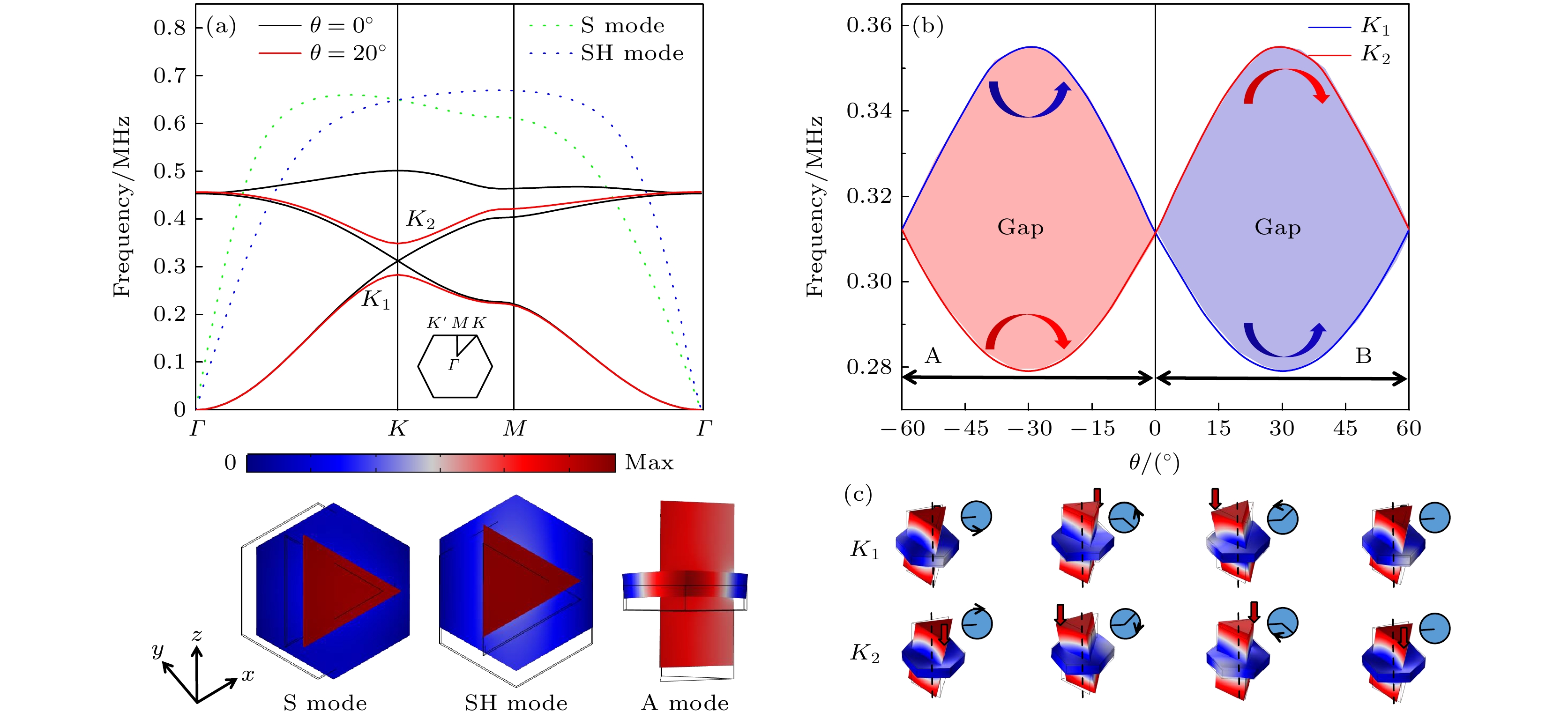
图 2 (a) 散射体高度
$h = 0.28{\kern 1 pt} {\kern 1 pt} {\kern 1 pt} {\text{mm}}$ 时声子晶体的能带结构; (b)${K_1}$ ,${K_2}$ 能谷频率随散射体角度的变化, 红色箭头和绿色箭头分别表示散射体顺时针和逆时针手征性回转; (c)$\theta = 20^\circ $ 时${K_1}$ ,${K_2}$ 谷每一帧图形经过三分之一周期的位移场, 黑色虚线是中轴线, 红色箭头表示每一帧散射体位移的最大位置Fig. 2. (a) Band structure of the phonon crystal with the height of scatter
$h = 0.28{\kern 1 pt} {\kern 1 pt} {\kern 1 pt} {\text{mm}}$ ; (b) variation of valley frequencies of${K_1}$ and${K_2}$ with the change of scatterer angle, red arrows and green arrows indicate clockwise and counterclockwise scatterer hand sign slewing respectively; (c) the displacement fields of${K_1}$ and${K_2}$ at$\theta = 20^\circ $ for each frame of the graph after one-third of the period, the black dashed line is the central axis, and the red arrow indicates the maximum position of the scatterer displacement for each frame.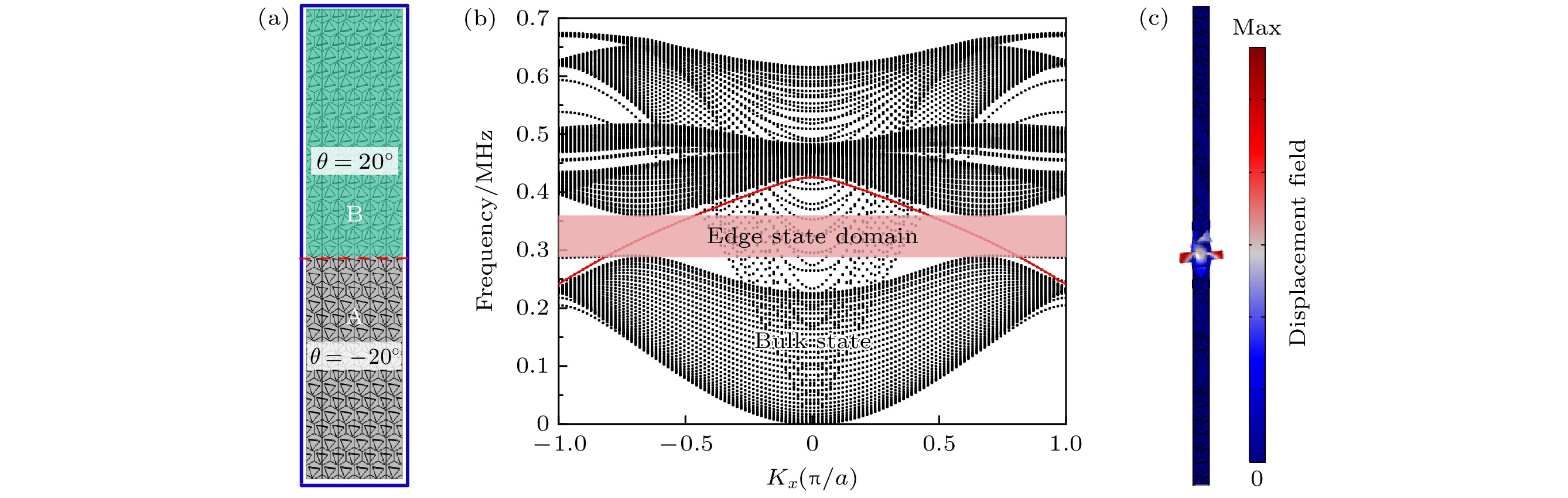
图 3 (a)由A和B相声子晶体组成的条形超胞, 红色虚线表示两相界面; (b) 超胞沿
$\varGamma {\text{-}}K$ 方向的投影能带结构, 浅灰色区域为体态结构, 浅红色区域为边缘态区域, 红色实线为连接上、下体态的边缘态; (c)条形超胞在边缘态频率的位移场Fig. 3. (a) Bar-shaped supercell composed of phonon crystals of A phase and B phase. The red dashed line indicates the interface; (b) the projected band structure of the supercell along the
$\varGamma {\text{-}}K$ direction, the light grey region is the bulk structure, the light red region is the edge state region, and the red solid line is the edge state; (c) displacement field of the strip supercell at the edge state frequency.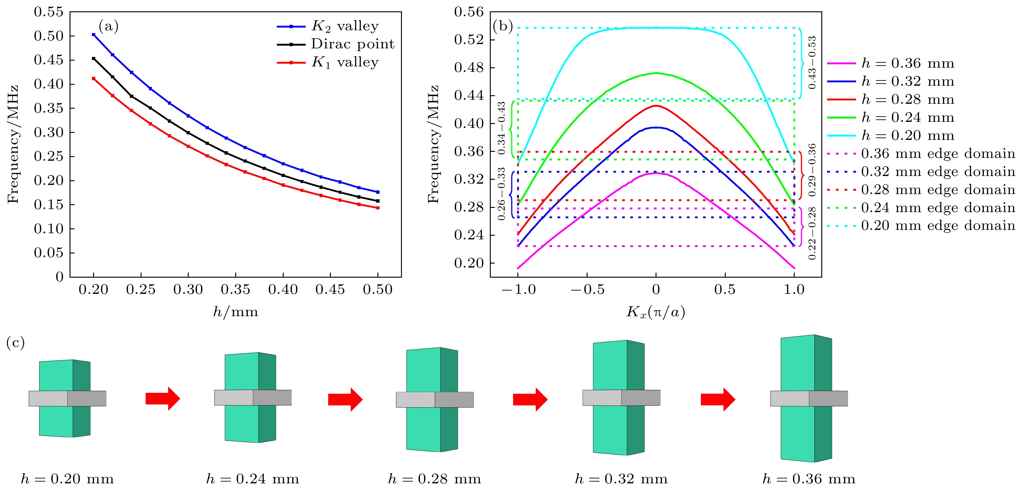
图 4 (a)狄拉克点及上、下能谷的频率随着散射体高度的变化; (b)各散射体高度下对应的边缘态, 其中相同颜色虚线则对应的是该散射体高度下的边缘态区域; (c)散射体连续变化示意图
Fig. 4. (a) Frequency of the Dirac point and the upper and lower valleys with different scatterer height; (b) the edge state at each scatterer height, where the same color dashed line corresponds to the edge state region at that scatterer height; (c) schematic diagram of continuous change of scatterer.

图 5 (a)由B, A相声子晶体组成的矩形超胞, 红色虚线表示两相界面, 红色五角星为点源; (b) 激励频率为0.33 MHz时的边缘态位移场; (c)当散射体高度h = 0.20, 0.24 , 0.32, 0.36 mm时, 对应的中心带隙频率激发边缘态的位移场
Fig. 5. (a) A rectangular supercell composed of crystal B and A, the red dotted line represents the interface between the two phases, and the red pentagram is the point source; (b) displacement field of edge state when excitation frequency is 0.33 MHz; (c) when the scatterer height h = 0.20, 0.24 , 0.32, 0.36 mm, the displacement field of the edge state excited by the frequency of the corresponding central band gap.
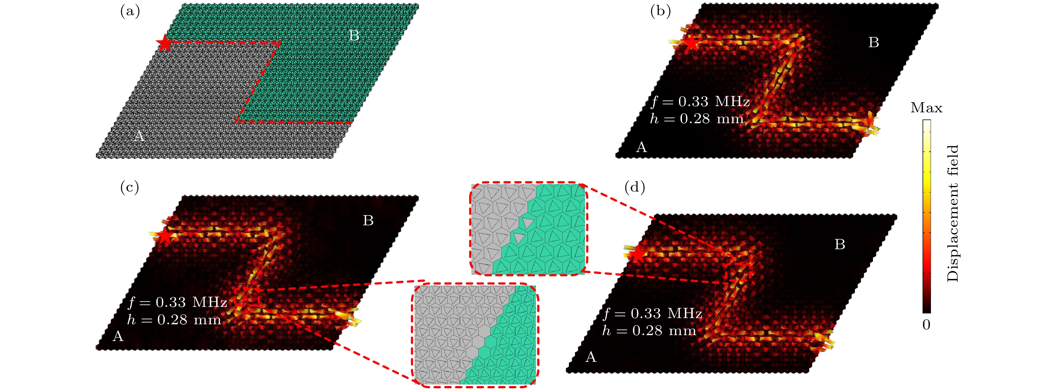
图 6 (a) B-A相声子晶体组成的“Z”字形界面超胞, 红色虚线为两相界面, 红色五角星为点源; (b)频率为0.33 MHz的点源激励的边缘态位移场; (c), (d)引入空腔和无序后边缘态的位移场分布, 插图部分为界面结构放大图
Fig. 6. (a) The Z shaped interface supercell was composed by B-A crystal, the red dotted line is the two-phase interface, and the red pentacle is the point source; (b) edge state displacement field of point source excitation with frequency of 0.33 MHz; (c), (d) the distribution of edge state displacement field after the introduction of cavity and disordered respectively; the part in the illustration is an enlarged view of interface structure.
-
[1] Klitzing K V, Dorda G, Pepper M 1980 Phys. Rev. Lett. 45 494
Google Scholar
[2] Bernevig B A, Hughes T L, Zhang S C 2006 Science 314 1757
Google Scholar
[3] Lu J, Qiu C, Ye L, Fan X, Ke M, Zhang F, Liu Z 2017 Nat. Phys. 13 369
Google Scholar
[4] Xiao D, Yao W, Niu Q 2007 Phys. Rev. Lett. 99 236809
Google Scholar
[5] Vila J, Pal R K, Ruzzene M 2017 Phys. Rev. B 96 134307
Google Scholar
[6] Chen Y, Liu X, Hu G 2019 J Mech Phys Solids 122 54
Google Scholar
[7] Gao N, Qu S, Si L, Wang J, Chen W 2021 Appl. Phys. Lett. 118 063502
Google Scholar
[8] Zhang Q, Chen Y, Zhang K, Hu G 2020 Phys. Rev. B 101 014101
Google Scholar
[9] Machon T, Alexander G P, Goldstein R E, Pesci A I 2016 Phys. Rev. Lett. 117 017801
Google Scholar
[10] Schaibley J R, Yu H Y, Clark G, Rivera P, Ross J S, Seyler K L, Yao W, Xu X 2016 Nat. Rev. Mater. 1 16055
Google Scholar
[11] Gorbachev R, Song J, Yu G, Kretinin A, Withers F, Cao Y, Mishchenko A, Grigorieva I, Novoselov K S, Levitov L 2014 Science 346 448
Google Scholar
[12] Wang Y T, Luan P G, Zhang S 2015 New J. Phys. 17 073031
Google Scholar
[13] Yan M, Lu J, Li F, Deng W, Huang X, Ma J, Liu Z 2018 Nat. Mater. 17 993
Google Scholar
[14] He C, Ni X, Ge H, Sun X C, Chen Y B, Lu M H, Liu X P, Chen Y F 2016 Nat. Phys. 12 1124
Google Scholar
[15] Noh J, Huang S, Chen K P, Rechtsman M C 2018 Phys. Rev. Lett. 120 063902
Google Scholar
[16] Collins M J, Zhang F, Bojko R, Chrostowski L, Rechtsman M C 2016 Phys. Rev. A 94 063827
Google Scholar
[17] Mak K F, McGill K L, Park J, McEuen P L 2014 Science 344 1489
Google Scholar
[18] Martin I, Blanter Y M, Morpurgo A 2008 Phys. Rev. Lett. 100 036804
Google Scholar
[19] Jung J, Zhang F, Qiao Z, MacDonald A H 2011 Phys. Rev. B 84 075418
Google Scholar
[20] Lu J, Qiu C, Ke M, Liu Z 2016 Phys. Rev. Lett. 116 093901
Google Scholar
[21] Yantchev V, Katardjiev I 2013 J. Micromech. Microeng. 23 043001
Google Scholar
[22] Tian Z H, Shen C, Li J F, et al. 2020 Nat. Commun. 11 762
Google Scholar

 下载:
下载:


计量
- 文章访问数: 7707
- PDF下载量: 179
- 被引次数: 0
