


-
构建了覆盖度为2.778%的黑磷烯吸附硅原子模型, 基于密度泛函理论计算了模型的电子特性, 并通过应力及电场对其电子特性进行调控. 研究表明: 当前研究的覆盖度下, Si原子的吸附导致黑磷烯几何对称性被破坏, 加剧了体系内的电荷转移, 完成轨道再杂化. 使黑磷烯带隙消失, 实现了其由半导体向准金属的转变. 其稳定的吸附位是位于P原子环中间的H位. 拉伸和电场均降低了黑磷烯体系稳定性. 拉伸形变使黑磷烯吸附Si原子结构打开带隙, 且带隙与形变量成正比, 实现对其带隙的调控. 电场与拉伸共作用下, 电场的引入使黑磷烯吸附Si原子带隙变窄且完成体系由直接带隙向间接带隙的转变. 带隙依旧随形变量增加而增加. 吸附Si原子的黑磷烯体系带隙可调性高于未吸附体系, 且易于实现带隙的稳定调控.In this paper, a model of Si atom adsorbed on black phosphorene with a coverage of 2.778% is constructed and the electronic properties of the model are calculated based on density functional theory. Moreover, the electronic properties are regulated by stress and electric field. Under the coverage of the current research, the results show that the adsorption of Si atoms results in the destruction of the black phosphorene’s geometric symmetry, which intensifies the charge transfer in the system and completes the orbital re-hybrid. The band gap of black phosphorene thus disappears and the transition from semiconductor to quasi metal is completed. The stable adsorption is at the H site in the middle of the P atomic ring. Both tensile field and electric field reduce the stability of the system. Owing to the tensile deformation, the band gap is opened by the structure of Si atom adsorbed on black phosphorene. And since the band gap is proportional to the deformation variable, it can be regulated and controlled. Under the combined action of electric field and tensile, the introduction of the electric field leads the band gap of Si adsorbed on black phosphorene system to be narrowed and the transition from the direct band gap to an indirect one to be completed. The band gap still goes up in proportion to the increase of deformation. The band gap of Si atom adsorbed on black phosphorene system is more adjustable than that of the Si atom that is not adsorbed on black phosphorene system, and the stable adjustment of the band gap is more likely to be realized.
[1] Li L, Yu Y, Ye G J, Ge Q, Ou X, Wu H, Feng D, Chen X H, Zhang Y 2014 Nat. Nanotechnol. 9 372
 Google Scholar
[2] Liu H, Neal A T, Zhu Z, Luo Z, Xu X, Tománek D, Ye P D 2014 ACS Nano 8 4033
Google Scholar
[3] James B, Matin A, Joy C, Chen Y Z, Ho A G, Valerio A, Raj S V, Yang G, Crozier K B, Yu-Lun C 2018 Nat. Photonics 12 601
Google Scholar
[4] Avsar A, Tan J Y, Kurpas M, Gmitra M, Watanabe K, Taniguchi T, Fabian J, Özyilmaz B 2017 Nat. Phys. 13 888
Google Scholar
[5] Li L, Yang F, Ye G J, Zhang Z, Zhu Z, Lou W, Zhou X, Li L, Watanabe K, Taniguchi T, Chang K, Wang Y, Chen X H, Zhang Y 2016 Nat. Nanotechnol. 11 593
Google Scholar
[6] Chen X, Lu X, Deng B, Sinai O, Shao Y, Li C, Yuan S, Tran V, Watanabe K, Taniguchi T, Naveh D, Yang L, Xia F 2017 Nat. Commun. 8 1672
Google Scholar
[7] Youngblood N, Chen C, Koester S J, Li M 2015 Nat. Photonics 9 247
Google Scholar
[8] Xia F, Wang H, Jia Y 2014 Nat. Commun. 5 4458
Google Scholar
[9] Deng B, Tran V, Xie Y, Hao J, Cheng L, Guo Q, Wang X, He T, Koester S J, Han W 2017 Nat. Commun. 8 14474
Google Scholar
[10] Buscema M, Groenendijk D J, Steele G A, Zant H, Castellanos-Gomez A 2014 Nat. Commun. 5 4651
Google Scholar
[11] Feng X, Huang X, Chen L, Tan W C, Wang L, Ang K W 2018 Adv. Funct. Mater. 28 1801524
Google Scholar
[12] Huang L, Dong B, Guo X, Chang Y, Chen N, Huang X, Liao W, Zhu C, Wang H, Lee C, Ang K W 2018 ACS Nano 13 913
[13] Castellanos-Gomez A 2015 J. Phys. Chem. Lett. 6 4280
Google Scholar
[14] Rajabali M, Esfandiari M, Rajabali S, Vakili-Tabatabaei M, Mohajerzadeh S, Mohajerzadeh S 2020 Adv. Mater. Interfaces 7 2000774
Google Scholar
[15] Rajabali M, Mohajerzadeh S 2019 Phys. Status Solidi RRL 13 1900197
Google Scholar
[16] Xu Y, Shi X, Zhang Y, Zhang H, Zhang K, Huang Z, Xu X, Guo J, Zhang H, Sun L, Zheng Z, Pan A, Zhang K 2020 Nat. Commun. 11 1330
Google Scholar
[17] Soo-Yeon C, Youhan L, Hyeong-Jun K, Hyunju J, Jong-Seon K 2016 Adv. Mater. 28 7020
Google Scholar
[18] Tyagi D, Wang H, Huang W, Hu L, Tang Y, Guo Z, Ouyang Z, Zhang H 2020 Nanoscale 12 3535
Google Scholar
[19] Prajapati Y K, Pal S, Verma A, Saini J P 2019 IET Optoelectron. 13 196
Google Scholar
[20] Kumar R, Pal S, Verma A, Prajapati Y K, Saini J P 2020 Superlattices Microstruct. 145 106591
Google Scholar
[21] Kumar P, Gupta M, Singh K 2020 Silicon 12 2809
Google Scholar
[22] Hui W, Yi C 2012 Nano Today 7 414
Google Scholar
[23] Obrovac M N, Christensen L 2004 Electrochem. Solid-State Lett. 7 A93
Google Scholar
[24] Pinson M B, Bazant M Z 2012 J. Electrochem. Soc. 160 A243
Google Scholar
[25] Carvalho A, Neto A 2015 ACS Central Sci. 1 289
Google Scholar
[26] Carvalho A, Wang M, Zhu X, Rodin A S, Su H, Neto A C 2016 Nat. Rev. Mater. 1 16061
Google Scholar
[27] Zhang C, Yu M, Anderson G, Dharmasena R R, Sumanasekera G 2017 Nanotechnology 28 075401
Google Scholar
[28] Sun J, Lee H, Pasta M, Yuan H, Zheng G, Sun Y, Li Y, Cui Y 2015 Nat. Nanotechnol. 10 980
Google Scholar
[29] Park C M, Sohn H J 2007 Adv. Mater. 19 2465
Google Scholar
[30] Arie A A, Lee J K 2013 Materials Science Forum 737 80
Google Scholar
[31] Domi Y, Usui H, Shimizu M, Kakimoto Y, Sakaguchi H 2016 ACS Appl. Mater. Interfaces 8 7125
Google Scholar
[32] Kim J S, Choi W, Byun D, Lee J K 2012 Solid State Ionics 212 43
Google Scholar
[33] Song J O, Shim H T, Byun D J, Lee J K 2007 Solid State Phenom. 124-126 1063
Google Scholar
[34] Yan C, Liu Q, Gao J, Yang Z, He D 2017 Beilstein J. Nanotechnol. 8 222
Google Scholar
[35] 彭勃, 徐耀林, Fokko M 2017 物理化学学报 33 2127
Google Scholar
Peng B, Xu Y, Fokko M 2017 Acta Phys.-Chim. Sin. 33 2127
Google Scholar
[36] Shojaei F, Hahn J R, Kang H S 2016 J. Phys. Chem. C 120 17106
Google Scholar
[37] Olmedo E M, Garza C, Fomine S 2019 J. Mol. Model. 25 292
Google Scholar
[38] Segall M, Lindan P, Probert M J, Pickard C J, Hasnip P J, Clark S J, Payne M C 2002 J. Phys. Condens. Matter 14 2717
Google Scholar
[39] Perdew J P, Burke K, Ernzerhof M 1998 Phys. Rev. Lett. 77 3865
Google Scholar
[40] Heyd J, Scuseria G E 2003 J. Chem. Phys. 118 8207
Google Scholar
[41] Luo Y, Ren C, Wang S, Li S, Zhang P, Yu J, Sun M, Sun Z, Tang W 2018 Nanoscale Res. Lett. 13 282
Google Scholar
[42] 曾祥明, 鄢慧君, 欧阳楚英 2012 物理学报 61 247101
Google Scholar
Zeng X M, Yan H J, Ouyang C Y 2012 Acta Phys. Sin. 61 247101
Google Scholar
[43] Mu G Y, Liu G L, Zhang G Y 2020 Int. J. Mod. Phys. B 34 2050191
Google Scholar
[44] Du Y, Ouyang C, Shi S, Lei M 2010 J. Appl. Phys. 107 0937181
Google Scholar
[45] Ge X, Zhou X H, Ye X, Chen X S 2020 Chem. Phys. Lett. 740 137075
Google Scholar
[46] Durajski A P, Gruszka K M, Niegodajew P 2020 Appl. Surf. Sci. 532 147377
Google Scholar
[47] El-Hachimi A G, Oubram O, Sadoqi M 2020 Superlattices Microstruct. 146 106673
Google Scholar
[48] Xu Y, Liu G, Xing S, Zhao G, Yang J 2020 J. Mater. Chem. C 8 14902
Google Scholar
[49] Zhou Y, Zhang M, Guo Z Miao L 2017 Mater. Horiz. 4 997
Google Scholar
[50] 谭兴毅, 王佳恒, 朱祎祎, 左安友, 金克新 2014 物理学报 63 207301
Google Scholar
Tan X Y, Wang J H, Zhu Y Y, Zuo A Y, Jin K X 2014 Acta Phys. Sin. 63 207301
Google Scholar
[51] Hou X H, Deng Z C, Zhang K 2017 Physica E 88 252
Google Scholar
[52] Ferrari A C, Meyer J C, Scardaci V 2006 Phys. Rev. Lett. 97 187401
Google Scholar
[53] Wang J X, Wang Y, Liu G L, Wei L, Zhang G Y 2020 Physica B 578 411755
Google Scholar
[54] 陈献, 程梅娟, 吴顺情, 朱梓忠 2017 物理学报 66 107102
Google Scholar
Chen X, Cheng M J, Wu S Q, Zhu Z Z 2017 Acta Phys. Sin. 66 107102
Google Scholar
[55] Sabzyan H, Sadeghpour N 2016 Z. Naturforsch. , A:Phys. Sci. 72 1
Google Scholar
[56] 张国英, 焦兴强, 刘业舒, 张安国, 孟春雪 2020 物理学报 69 237101
Zhang G Y, Jiao X Q, Liu Y S, Zhang A G, Meng C X 2020 Acta Phys. Sin. 69 237101
[57] Tran V, Soklaski R, Liang Y, Yang L 2014 Phys. Rev. B 89 235319
Google Scholar
[58] Rodin A S, Carvalho A, Neto A 2014 Phys. Rev. Lett. 112 176801
Google Scholar
[59] Gazzari S, Wrighton-Araneda K, Cortés-Arriagada D 2020 Surf. Interfaces 21 100786
Google Scholar
[60] Carmel S, Subramanian S, Rathinam R, Bhattacharyya A 2020 J. Appl. Phys. 127 094303
Google Scholar
[61] Cakır D, Sahin H, Peeters F M 2014 Phys. Rev. B 90 205421
Google Scholar
[62] Xie Z, Hui L, Wang J, Zhu G, Chen Z, Li C 2018 Comput. Mater. Sci. 144 304
Google Scholar
[63] Yan L, Yang S, Li J 2014 J. Phys. Chem. C 118 23970
Google Scholar
[64] Yu W Z, Yan J A, Gao S P 2015 Nanoscale Res. Lett. 10 351
Google Scholar
[65] Lü H Y, Lu W J, Shao D F, Sun Y P 2014 Phys. Rev. B 90 085433
Google Scholar
[66] Fei R, Yang L 2014 Nano Lett. 14 2884
Google Scholar
[67] Kumar P, Bhadoria B S, Kumar S, Bhowmick S, Chauhan Y S, Agarwal A 2016 Phys. Rev. B 93 195428
Google Scholar
[68] Peng X, Wei Q, Copple A 2014 Phys. Rev. 90 0854021
Google Scholar
[69] Karki B, Freelon B, Rajapakse M, Musa R, Riyadh S, Morris B, Abu U, Yu M, Sumanasekera G, Jasinski J B 2020 Nanotechnology 31 425707
Google Scholar
[70] Li Y, Hu Z, Lin S, Lai S K, Wei J, Shu P L 2017 Adv. Funct. Mater. 27 1600986
Google Scholar
[71] Luis V G, Riccardo F, Andres C G 2019 Nanoscale 11 12080
Google Scholar
[72] Liang S, Hasan M, Seo J H 2019 Nanomaterials 9 566
Google Scholar
[73] Singh V, Joung D, Lei Z, Das S, Khondaker S I, Seal S 2011 Prog. Mater. Sci. 56 1178
Google Scholar
[74] Wang Y, Yang R, Shi Z, Zhang L, Shi D, Wang E, Zhang G 2011 ACS Nano 5 3645
Google Scholar
[75] Tang H M, Gao S P 2019 Comput. Mater. Sci. ence 158 88
Google Scholar
[76] 杨兆曜2017 硕士学位论文 (无锡: 江南大学)
Yang Z Y 2017 M. D. Thesis (Wuxi: Jiangnan University) (in Chinese)
[77] Jiang J W, Park H S 2014 Nat. Commun. 5 4727
Google Scholar
-
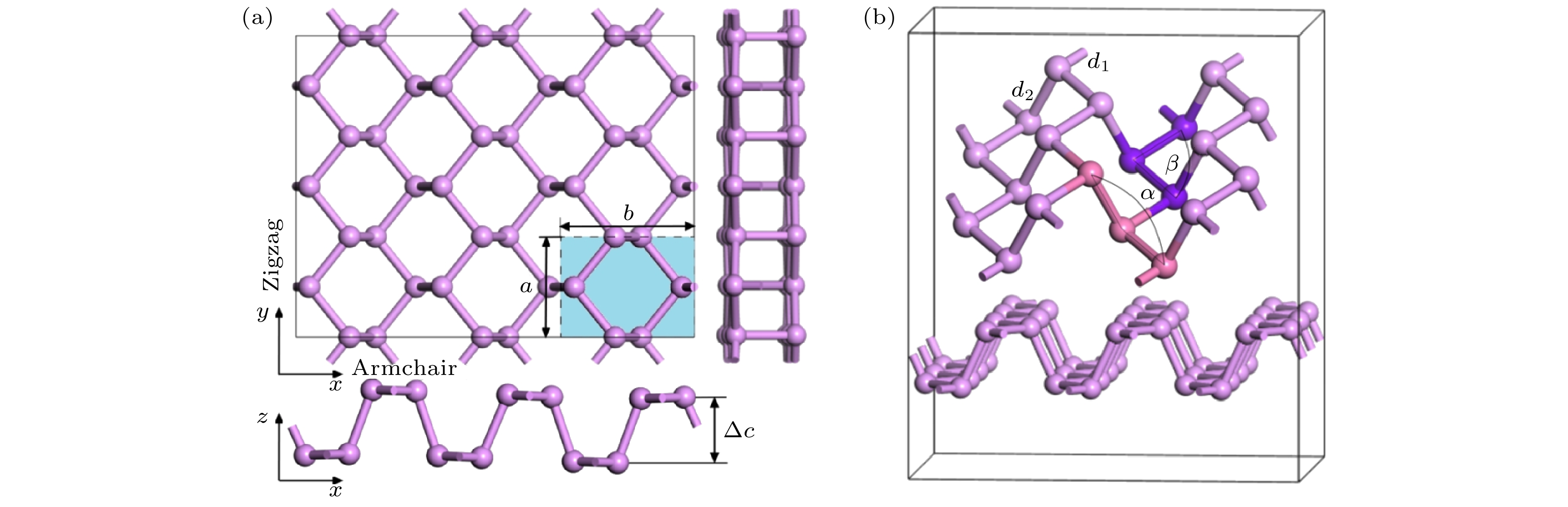
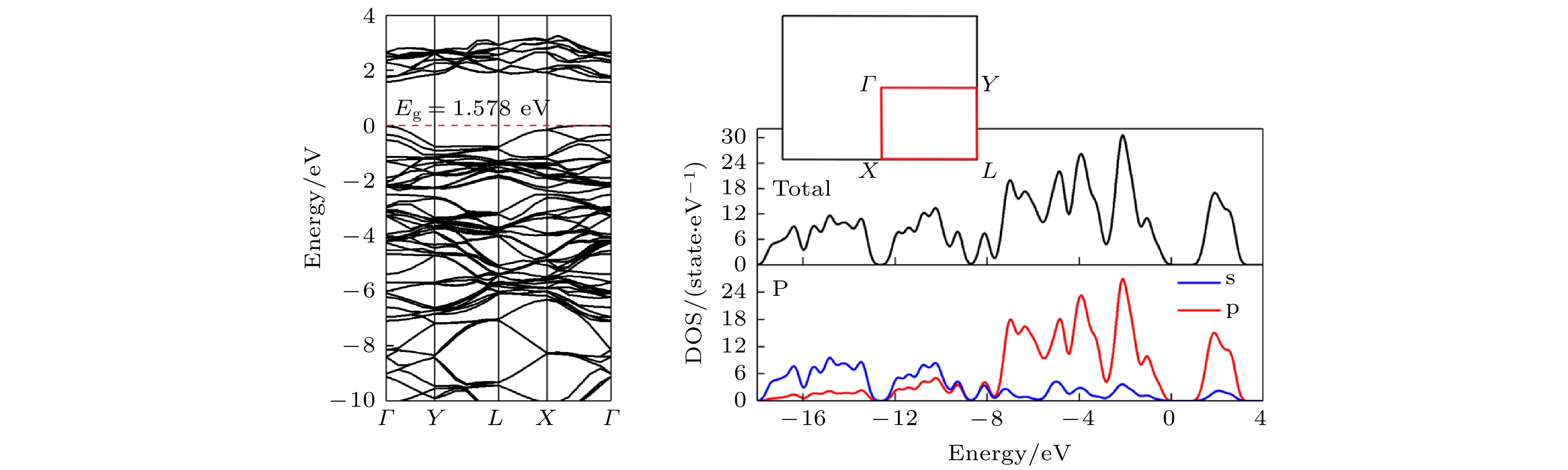
图 1 本征黑磷烯模型 (a)黑磷烯的主视图、俯视图、侧视图; (b)黑磷烯结构示意图
Fig. 1. Intrinsic black phosphorene model: (a) Front view, top view, and side view of black phosphorene; (b) schematic diagram of the structure of black phosphorene.
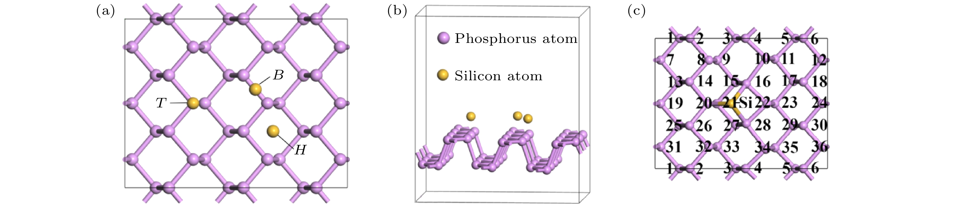
图 3 黑磷烯吸附Si原子模型 (a)主视图; (b)示意图; (c) P原子编号示意图
Fig. 3. Si adsorbed on black phosphorene model: (a) Main view; (b) diagrammatic sketch; (c) numbering diagram of P atom.
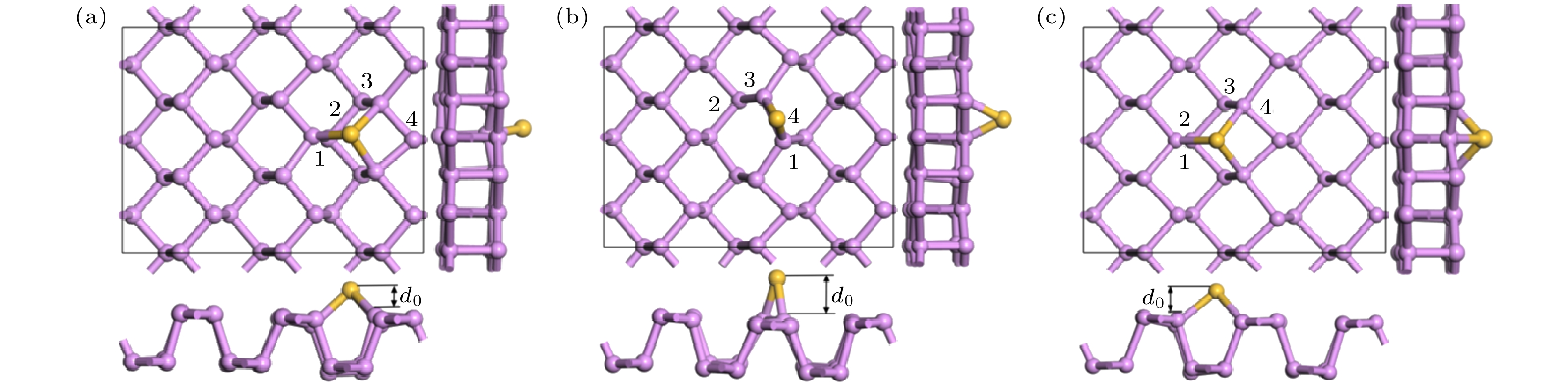
图 4 黑磷烯吸附Si原子模型几何优化结构 (a) T位; (b) B位; (c) H位
Fig. 4. Geometry optimization of Si adsorbed on black phosphorene model: (a) T site; (b) B site; (c) H site.
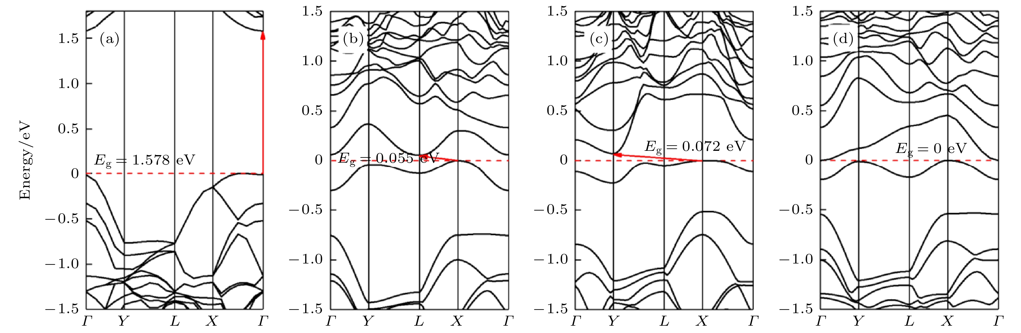
图 5 黑磷体系能带结构 (a)本征黑磷烯; (b) T位吸附; (c) B位吸附; (d) H位吸附
Fig. 5. Band structure of black phosphorene system: (a) Intrinsic black phosphorene; (b) T site adsorption; (c) B site adsorption; (d) H site adsorption.
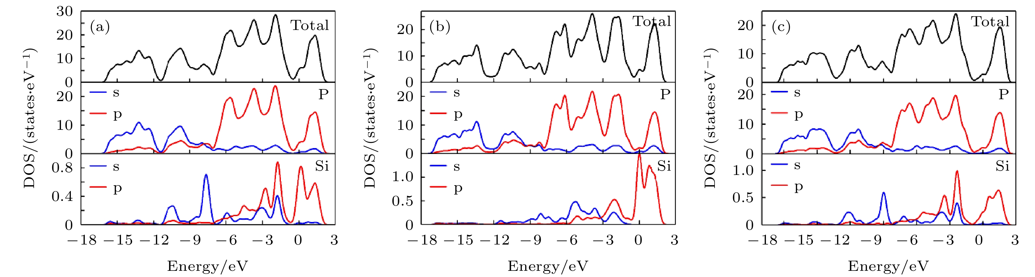
图 6 黑磷烯吸附体系DOS (a) T位; (b) B位; (c) H位
Fig. 6. The DOS of Si adsorbed on black phosphorene system: (a) T site; (b) B site; (c) H site.
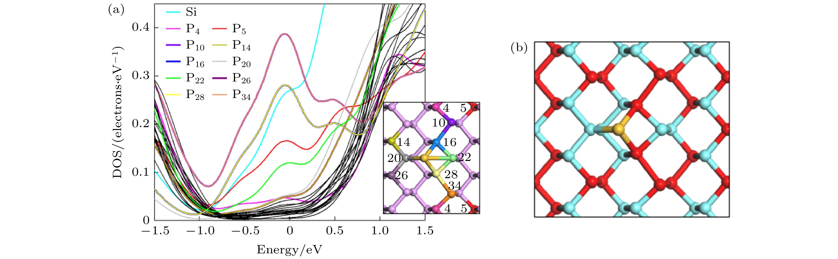
图 7 (a)单个P原子DOS图; (b) P原子得失电子示意图; 红色球体代表得到电子的P原子, 蓝色球体代表失去电子的P原子
Fig. 7. (a) DOS diagram of single P atom; (b) schematic diagram of gain and loss of electrons of P atom. The red sphere represents the P atom that gets electrons, and the blue sphere represents the P atom that loses electrons.
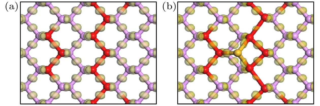
图 8 黑磷烯电荷差分密度图 (a)本征黑磷烯; (b)黑磷烯吸附Si原子
Fig. 8. Differential charge density of the black phosphorene: (a) Intrinsic black phosphorene; (b) Si adsorbed on black phosphorene system.
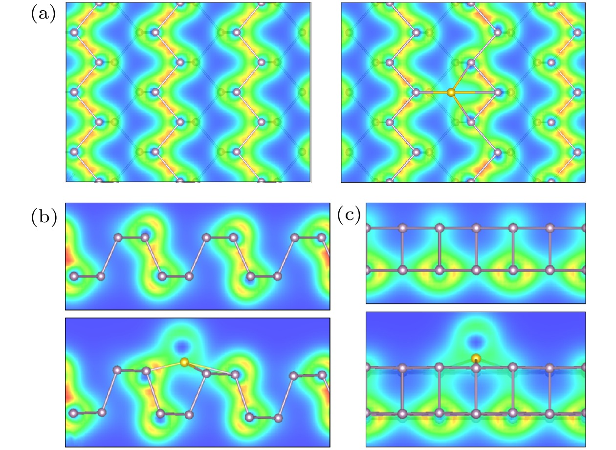
图 9 本征黑磷烯与黑磷烯吸附体系电荷密度图 (a)主视图; (b)俯视图; (c)侧视图
Fig. 9. Charge density diagram of the adsorption system of intrinsic black phosphorene and black phosphorene: (a) Main view; (b) top view; (c) side view.
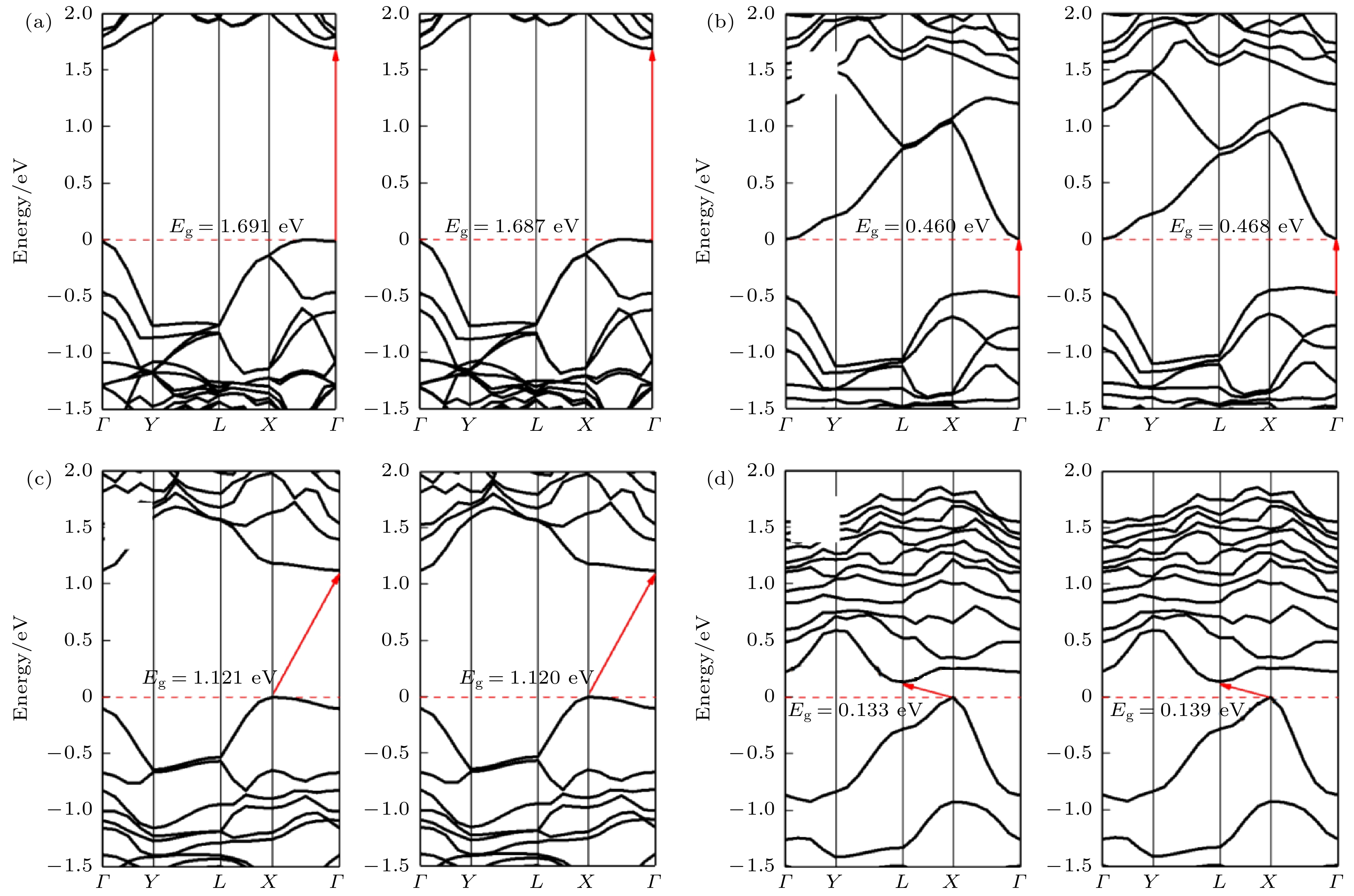
图 10 考虑泊松比前后、拉伸形变量为2%的黑磷烯能带结构 (a)纯黑磷烯; (b)黑磷烯吸附Si原子; (c)电场与形变共作用的纯黑磷烯; (d) 电场与形变共作用的黑磷烯吸附Si原子
Fig. 10. Band structure of black phosphorene with 2% tensile deformation before and after considering Poisson’s ratio (a) Pure BP, (b) Si absorbed on BP, (c) pure BP with co-action of electric field and deformation, (d) Si absorbed on BP with co-action of electric field and deformation.
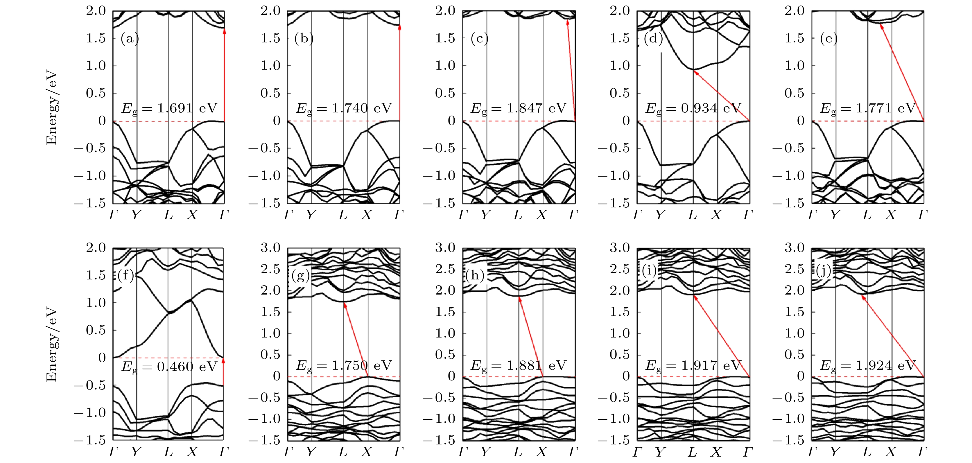
图 11 (a)—(e)拉伸形变量为2%—10%的黑磷烯能带结构; (f)—(j)拉伸形变量为2%—10%的黑磷烯吸附Si原子体系能带结构
Fig. 11. (a)−(e) Band structure of black phosphorene with 2%−10% tensile deformation; (f)−(j) band structure of Si adsorbed on black phosphorene with 2%−10% tensile deformation.
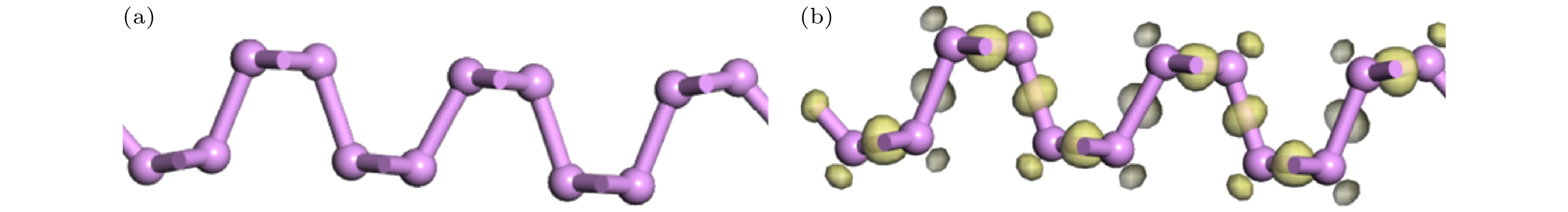
图 12 (a)形变为8%的黑磷烯结构俯视图; (b)形变为8%的黑磷烯电荷差分密度
Fig. 12. (a) Top view of the structure of 8% tensile deformation black phosphorene; (b) differential charge density of 8% tensile deformation phosphorene.
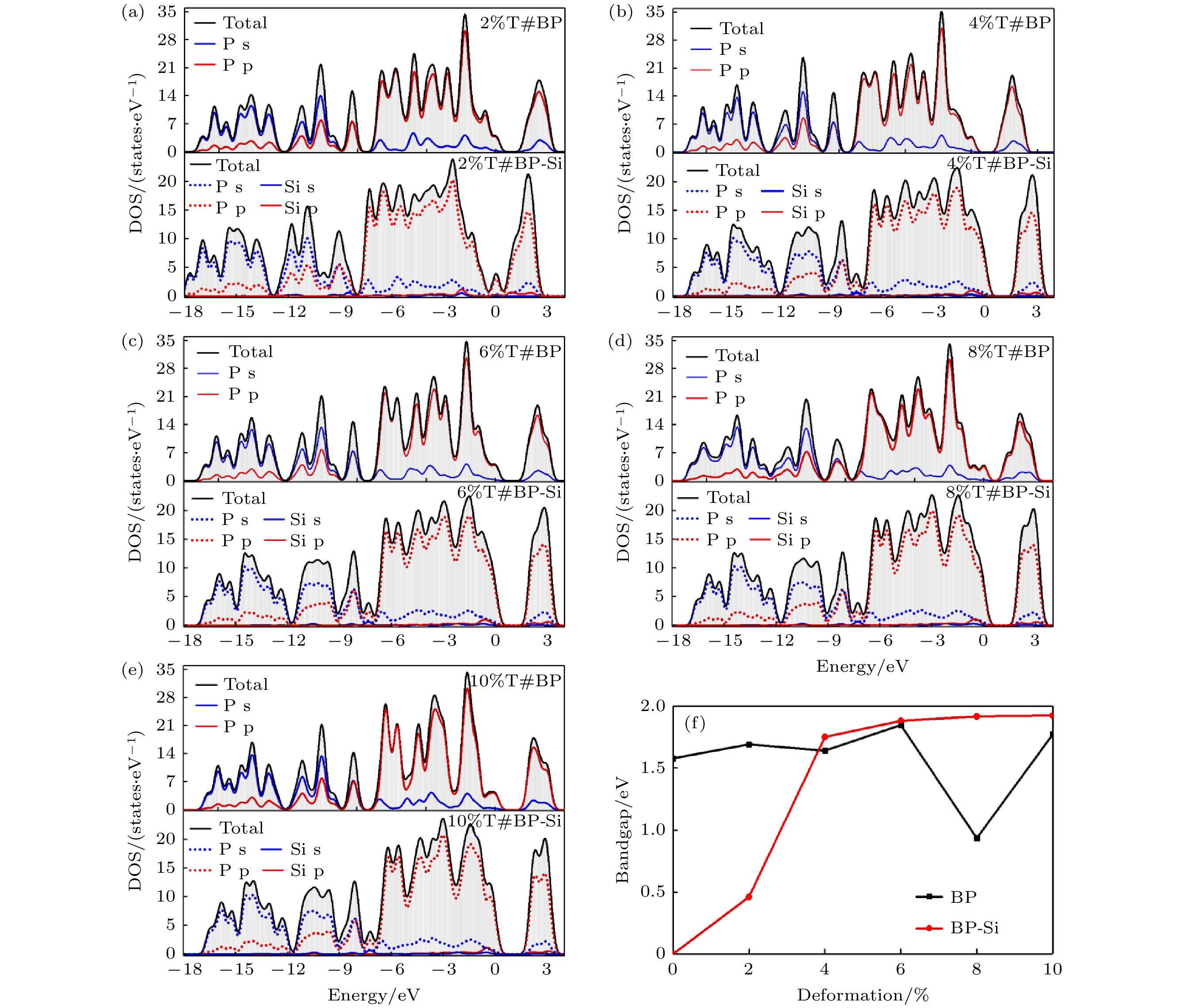
图 13 (a)—(e)拉伸形变量为2%—10%的纯黑磷烯(BP)以及黑磷烯吸附Si原子体系(BP-Si)态密度结构; (f)黑磷烯带隙变化曲线
Fig. 13. (a)−(e) The DOS of black phosphorene (BP) and Si adsorbed on black phosphorene (BP-Si) with 2%−10% tensile deformation; (f) band gap curves of black phosphorene.
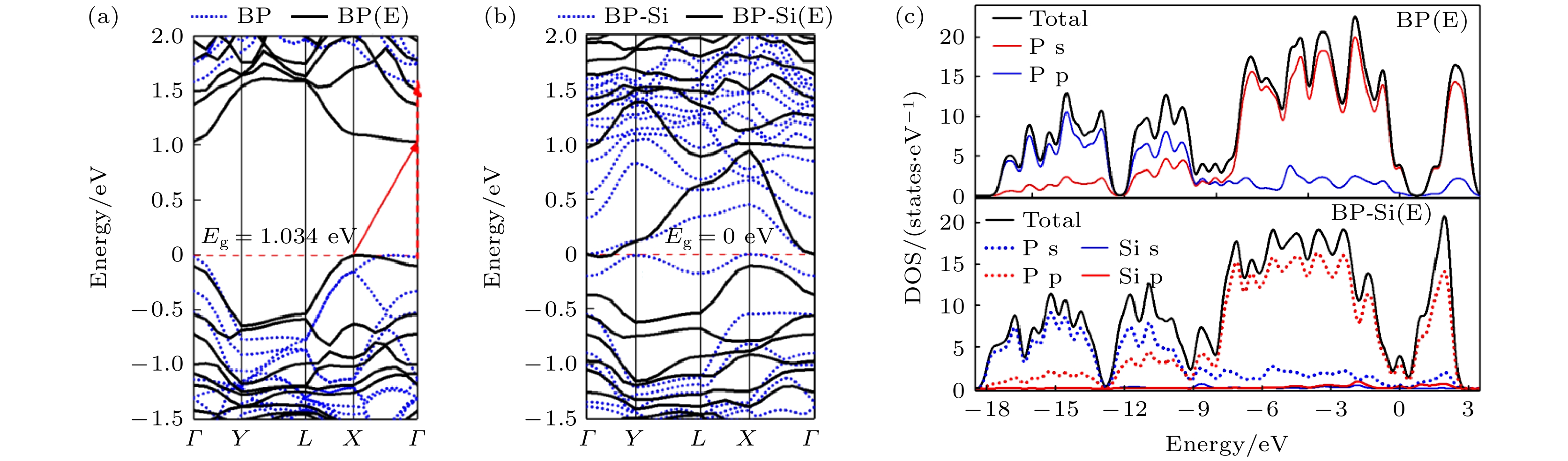
图 14 电场作用下纯黑磷烯与黑磷烯吸附Si原子体系 (a), (b)能带结构, 其中蓝色虚线代表黑磷及黑磷烯吸附体系的能带结构, 黑色实现代表电场作用下黑磷烯及其吸附体系的能带结构; (c) DOS结构
Fig. 14. Si adsorbed on black phosphorene system and pure black phosphorene under electric field: (a), (b) Band structure, the blue dotted line represents the energy band structure of black phosphorus and black phosphorene adsorption system, and the black realization represents the energy band structure of black phosphorus and its adsorption system under the action of electric field; (c) DOS.
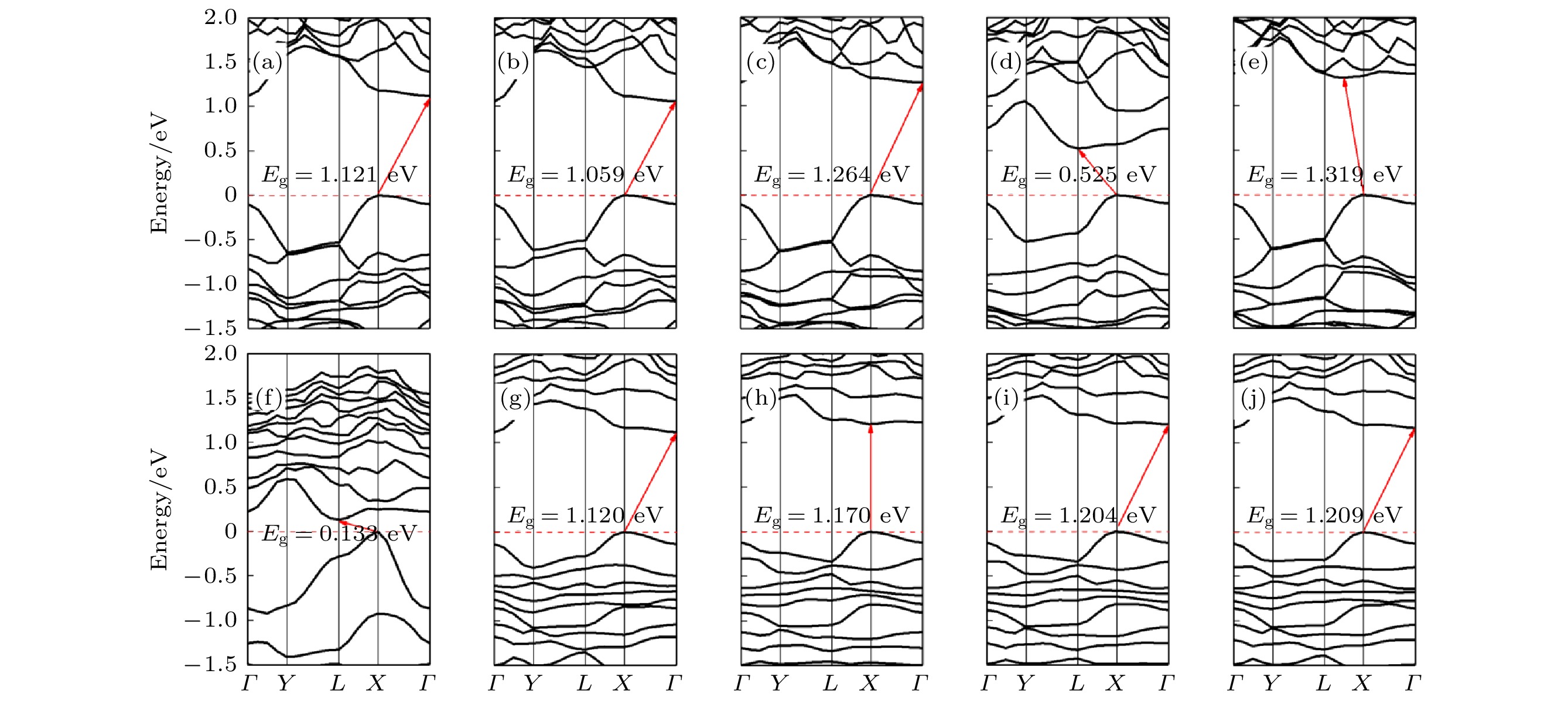
图 15 (a)—(e)电场作用下拉伸形变量为2%—10%的黑磷烯能带结构; (f)—(j)电场作用下拉伸形变量为2%—10%的黑磷烯吸附Si原子体系能带结构
Fig. 15. (a)−(e) Band structure of black phosphorene with 2%−10% tensile deformation under electric field; (f)−(j) band structure of Si adsorbed on black phosphorene system with 2%−10% tensile deformation under electric field.
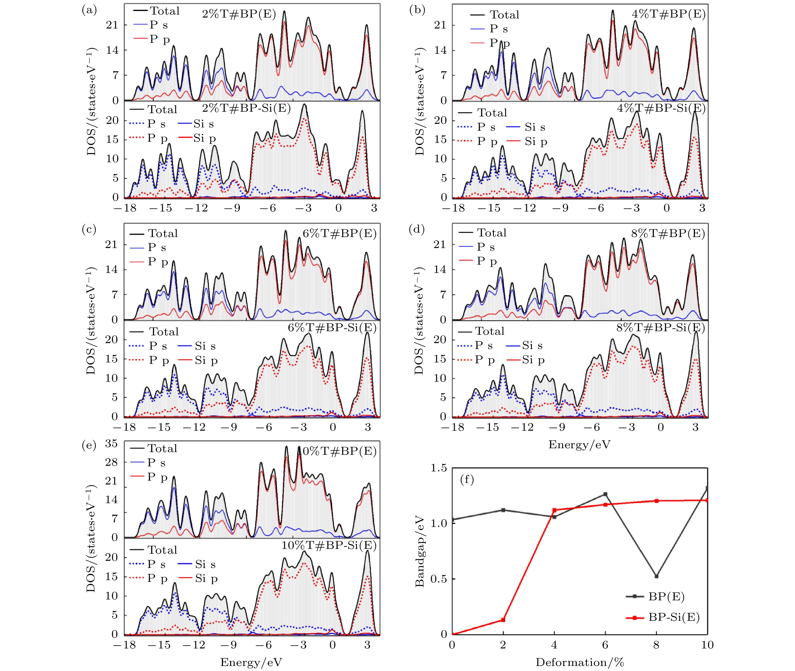
图 16 (a)—(e)电场作用下拉伸形变量为2%—10%的黑磷烯吸附Si原子体系能带结构; (f)黑磷烯带隙变化曲线
Fig. 16. (a)−(e) Band structure of Si adsorbed on black phosphorene system with 2%−10% tensile deformation under the action of electric field; (f) band gap curves of black phosphorene.
表 1 吸附原子所在原子环的P—P键键长与Si原子吸附高度
Table 1. Relationship between P—P bond length and Si adsorption height.
吸附位 P—Si/ P—P(1)/Å P—P(2)/Å P—P(3)/Å P—P(4)/Å d0/Å T 2.283 2.214 2.206 2.206 2.207 1.138 B 2.236 2.256 2.186 2.236 2.212 1.880 H 2.312 2.221 2.200 2.204 2.230 1.160  下载: 导出CSV
表 2 P原子间键长及键级
Table 2. Bond length and bond order between P atoms.
P4—P10, P34—P4 P10—P16, P28—P34 P16—P22, P22—P28 本征P—P P16, 28—Si P20—Si 键长/Å 2.162 2.497 2.210 2.210 2.331 2.312 键级 0.48 1.00 0.45 0.47 0.42 0.33
下载: 导出CSV
表 3 P原子的Mulliken电荷布居数
Table 3. Mulliken charge population of P atom.
原子编号 P10, 34 P16, 28 P11, 35 P8, 12, 13, 25, 32, 36 P1, 7, 9, 17, 24, 29, 31, 33 P2, 15, 18, 19, 23, 27, 30 P3, 4, 14, 26 P5, 22 P6 P20 P21 Si Total/e 5.10 5.06 5.04 5.02 5.01 4.99 4.98 4.97 4.96 4.94 4.93 3.78 Charge/e –0.10 –0.06 –0.04 –0.02 –0.01 0.01 0.02 0.03 0.04 0.06 0.07 0.22
下载: 导出CSV
表 4 拉伸形变作用下纯黑磷烯单原子结合能和黑磷烯吸附Si原子吸附能
Table 4. Monoatomic binding energy of black phosphorene and adsorption energy of Si adsorbed on black phosphorene under tensile deformation.
形变量/% 0 2 4 6 8 10 结合能/eV –5.774 –5.755 –5.719 –5.703 –5.701 –5.688 吸附能/eV 3.970 3.914 3.864 3.683 3.652 3.657
下载: 导出CSV
表 5 电场与拉伸共作用下纯黑磷烯单原子结合能和黑磷烯吸附Si原子吸附能
Table 5. Single atom binding energy of black phosphorene and adsorption energy of Si adsorbed on black phosphorene system under the action of electric field and tensile.
形变量/% 0 2 4 6 8 10 结合能/eV –2.507 –2.485 –2.457 –2.439 –2.433 –2.421 吸附能/eV 3.461 3.420 3.366 3.254 3.214 3.210
下载: 导出CSV
-
[1] Li L, Yu Y, Ye G J, Ge Q, Ou X, Wu H, Feng D, Chen X H, Zhang Y 2014 Nat. Nanotechnol. 9 372
Google Scholar
[2] Liu H, Neal A T, Zhu Z, Luo Z, Xu X, Tománek D, Ye P D 2014 ACS Nano 8 4033
Google Scholar
[3] James B, Matin A, Joy C, Chen Y Z, Ho A G, Valerio A, Raj S V, Yang G, Crozier K B, Yu-Lun C 2018 Nat. Photonics 12 601
Google Scholar
[4] Avsar A, Tan J Y, Kurpas M, Gmitra M, Watanabe K, Taniguchi T, Fabian J, Özyilmaz B 2017 Nat. Phys. 13 888
Google Scholar
[5] Li L, Yang F, Ye G J, Zhang Z, Zhu Z, Lou W, Zhou X, Li L, Watanabe K, Taniguchi T, Chang K, Wang Y, Chen X H, Zhang Y 2016 Nat. Nanotechnol. 11 593
Google Scholar
[6] Chen X, Lu X, Deng B, Sinai O, Shao Y, Li C, Yuan S, Tran V, Watanabe K, Taniguchi T, Naveh D, Yang L, Xia F 2017 Nat. Commun. 8 1672
Google Scholar
[7] Youngblood N, Chen C, Koester S J, Li M 2015 Nat. Photonics 9 247
Google Scholar
[8] Xia F, Wang H, Jia Y 2014 Nat. Commun. 5 4458
Google Scholar
[9] Deng B, Tran V, Xie Y, Hao J, Cheng L, Guo Q, Wang X, He T, Koester S J, Han W 2017 Nat. Commun. 8 14474
Google Scholar
[10] Buscema M, Groenendijk D J, Steele G A, Zant H, Castellanos-Gomez A 2014 Nat. Commun. 5 4651
Google Scholar
[11] Feng X, Huang X, Chen L, Tan W C, Wang L, Ang K W 2018 Adv. Funct. Mater. 28 1801524
Google Scholar
[12] Huang L, Dong B, Guo X, Chang Y, Chen N, Huang X, Liao W, Zhu C, Wang H, Lee C, Ang K W 2018 ACS Nano 13 913
[13] Castellanos-Gomez A 2015 J. Phys. Chem. Lett. 6 4280
Google Scholar
[14] Rajabali M, Esfandiari M, Rajabali S, Vakili-Tabatabaei M, Mohajerzadeh S, Mohajerzadeh S 2020 Adv. Mater. Interfaces 7 2000774
Google Scholar
[15] Rajabali M, Mohajerzadeh S 2019 Phys. Status Solidi RRL 13 1900197
Google Scholar
[16] Xu Y, Shi X, Zhang Y, Zhang H, Zhang K, Huang Z, Xu X, Guo J, Zhang H, Sun L, Zheng Z, Pan A, Zhang K 2020 Nat. Commun. 11 1330
Google Scholar
[17] Soo-Yeon C, Youhan L, Hyeong-Jun K, Hyunju J, Jong-Seon K 2016 Adv. Mater. 28 7020
Google Scholar
[18] Tyagi D, Wang H, Huang W, Hu L, Tang Y, Guo Z, Ouyang Z, Zhang H 2020 Nanoscale 12 3535
Google Scholar
[19] Prajapati Y K, Pal S, Verma A, Saini J P 2019 IET Optoelectron. 13 196
Google Scholar
[20] Kumar R, Pal S, Verma A, Prajapati Y K, Saini J P 2020 Superlattices Microstruct. 145 106591
Google Scholar
[21] Kumar P, Gupta M, Singh K 2020 Silicon 12 2809
Google Scholar
[22] Hui W, Yi C 2012 Nano Today 7 414
Google Scholar
[23] Obrovac M N, Christensen L 2004 Electrochem. Solid-State Lett. 7 A93
Google Scholar
[24] Pinson M B, Bazant M Z 2012 J. Electrochem. Soc. 160 A243
Google Scholar
[25] Carvalho A, Neto A 2015 ACS Central Sci. 1 289
Google Scholar
[26] Carvalho A, Wang M, Zhu X, Rodin A S, Su H, Neto A C 2016 Nat. Rev. Mater. 1 16061
Google Scholar
[27] Zhang C, Yu M, Anderson G, Dharmasena R R, Sumanasekera G 2017 Nanotechnology 28 075401
Google Scholar
[28] Sun J, Lee H, Pasta M, Yuan H, Zheng G, Sun Y, Li Y, Cui Y 2015 Nat. Nanotechnol. 10 980
Google Scholar
[29] Park C M, Sohn H J 2007 Adv. Mater. 19 2465
Google Scholar
[30] Arie A A, Lee J K 2013 Materials Science Forum 737 80
Google Scholar
[31] Domi Y, Usui H, Shimizu M, Kakimoto Y, Sakaguchi H 2016 ACS Appl. Mater. Interfaces 8 7125
Google Scholar
[32] Kim J S, Choi W, Byun D, Lee J K 2012 Solid State Ionics 212 43
Google Scholar
[33] Song J O, Shim H T, Byun D J, Lee J K 2007 Solid State Phenom. 124-126 1063
Google Scholar
[34] Yan C, Liu Q, Gao J, Yang Z, He D 2017 Beilstein J. Nanotechnol. 8 222
Google Scholar
[35] 彭勃, 徐耀林, Fokko M 2017 物理化学学报 33 2127
Google Scholar
Peng B, Xu Y, Fokko M 2017 Acta Phys.-Chim. Sin. 33 2127
Google Scholar
[36] Shojaei F, Hahn J R, Kang H S 2016 J. Phys. Chem. C 120 17106
Google Scholar
[37] Olmedo E M, Garza C, Fomine S 2019 J. Mol. Model. 25 292
Google Scholar
[38] Segall M, Lindan P, Probert M J, Pickard C J, Hasnip P J, Clark S J, Payne M C 2002 J. Phys. Condens. Matter 14 2717
Google Scholar
[39] Perdew J P, Burke K, Ernzerhof M 1998 Phys. Rev. Lett. 77 3865
Google Scholar
[40] Heyd J, Scuseria G E 2003 J. Chem. Phys. 118 8207
Google Scholar
[41] Luo Y, Ren C, Wang S, Li S, Zhang P, Yu J, Sun M, Sun Z, Tang W 2018 Nanoscale Res. Lett. 13 282
Google Scholar
[42] 曾祥明, 鄢慧君, 欧阳楚英 2012 物理学报 61 247101
Google Scholar
Zeng X M, Yan H J, Ouyang C Y 2012 Acta Phys. Sin. 61 247101
Google Scholar
[43] Mu G Y, Liu G L, Zhang G Y 2020 Int. J. Mod. Phys. B 34 2050191
Google Scholar
[44] Du Y, Ouyang C, Shi S, Lei M 2010 J. Appl. Phys. 107 0937181
Google Scholar
[45] Ge X, Zhou X H, Ye X, Chen X S 2020 Chem. Phys. Lett. 740 137075
Google Scholar
[46] Durajski A P, Gruszka K M, Niegodajew P 2020 Appl. Surf. Sci. 532 147377
Google Scholar
[47] El-Hachimi A G, Oubram O, Sadoqi M 2020 Superlattices Microstruct. 146 106673
Google Scholar
[48] Xu Y, Liu G, Xing S, Zhao G, Yang J 2020 J. Mater. Chem. C 8 14902
Google Scholar
[49] Zhou Y, Zhang M, Guo Z Miao L 2017 Mater. Horiz. 4 997
Google Scholar
[50] 谭兴毅, 王佳恒, 朱祎祎, 左安友, 金克新 2014 物理学报 63 207301
Google Scholar
Tan X Y, Wang J H, Zhu Y Y, Zuo A Y, Jin K X 2014 Acta Phys. Sin. 63 207301
Google Scholar
[51] Hou X H, Deng Z C, Zhang K 2017 Physica E 88 252
Google Scholar
[52] Ferrari A C, Meyer J C, Scardaci V 2006 Phys. Rev. Lett. 97 187401
Google Scholar
[53] Wang J X, Wang Y, Liu G L, Wei L, Zhang G Y 2020 Physica B 578 411755
Google Scholar
[54] 陈献, 程梅娟, 吴顺情, 朱梓忠 2017 物理学报 66 107102
Google Scholar
Chen X, Cheng M J, Wu S Q, Zhu Z Z 2017 Acta Phys. Sin. 66 107102
Google Scholar
[55] Sabzyan H, Sadeghpour N 2016 Z. Naturforsch. , A:Phys. Sci. 72 1
Google Scholar
[56] 张国英, 焦兴强, 刘业舒, 张安国, 孟春雪 2020 物理学报 69 237101
Zhang G Y, Jiao X Q, Liu Y S, Zhang A G, Meng C X 2020 Acta Phys. Sin. 69 237101
[57] Tran V, Soklaski R, Liang Y, Yang L 2014 Phys. Rev. B 89 235319
Google Scholar
[58] Rodin A S, Carvalho A, Neto A 2014 Phys. Rev. Lett. 112 176801
Google Scholar
[59] Gazzari S, Wrighton-Araneda K, Cortés-Arriagada D 2020 Surf. Interfaces 21 100786
Google Scholar
[60] Carmel S, Subramanian S, Rathinam R, Bhattacharyya A 2020 J. Appl. Phys. 127 094303
Google Scholar
[61] Cakır D, Sahin H, Peeters F M 2014 Phys. Rev. B 90 205421
Google Scholar
[62] Xie Z, Hui L, Wang J, Zhu G, Chen Z, Li C 2018 Comput. Mater. Sci. 144 304
Google Scholar
[63] Yan L, Yang S, Li J 2014 J. Phys. Chem. C 118 23970
Google Scholar
[64] Yu W Z, Yan J A, Gao S P 2015 Nanoscale Res. Lett. 10 351
Google Scholar
[65] Lü H Y, Lu W J, Shao D F, Sun Y P 2014 Phys. Rev. B 90 085433
Google Scholar
[66] Fei R, Yang L 2014 Nano Lett. 14 2884
Google Scholar
[67] Kumar P, Bhadoria B S, Kumar S, Bhowmick S, Chauhan Y S, Agarwal A 2016 Phys. Rev. B 93 195428
Google Scholar
[68] Peng X, Wei Q, Copple A 2014 Phys. Rev. 90 0854021
Google Scholar
[69] Karki B, Freelon B, Rajapakse M, Musa R, Riyadh S, Morris B, Abu U, Yu M, Sumanasekera G, Jasinski J B 2020 Nanotechnology 31 425707
Google Scholar
[70] Li Y, Hu Z, Lin S, Lai S K, Wei J, Shu P L 2017 Adv. Funct. Mater. 27 1600986
Google Scholar
[71] Luis V G, Riccardo F, Andres C G 2019 Nanoscale 11 12080
Google Scholar
[72] Liang S, Hasan M, Seo J H 2019 Nanomaterials 9 566
Google Scholar
[73] Singh V, Joung D, Lei Z, Das S, Khondaker S I, Seal S 2011 Prog. Mater. Sci. 56 1178
Google Scholar
[74] Wang Y, Yang R, Shi Z, Zhang L, Shi D, Wang E, Zhang G 2011 ACS Nano 5 3645
Google Scholar
[75] Tang H M, Gao S P 2019 Comput. Mater. Sci. ence 158 88
Google Scholar
[76] 杨兆曜2017 硕士学位论文 (无锡: 江南大学)
Yang Z Y 2017 M. D. Thesis (Wuxi: Jiangnan University) (in Chinese)
[77] Jiang J W, Park H S 2014 Nat. Commun. 5 4727
Google Scholar

 下载:
下载:
计量
- 文章访问数: 6309
- PDF下载量: 82
- 被引次数: 0
