


-
采用一维自洽耦合流体模型理论研究了射频(rf)/直流(dc)驱动大气压氩气(Ar)介质阻挡放电特性, 仿真得到了不同直流电压下, 射频最小维持放电电压变化情况、周期平均电子密度平均值随周期平均气体电压平均值变化情况、电子产生率及电子密度的时空分布. 分析表明: 直流电压通过改变介质表面电荷密度来影响气隙电压, 从而控制放电过程. 直流电压较小时放电被抑制, 直流电压较大时放电得以恢复. 随着直流电压的增大, 射频最小维持放电电压振幅随之呈现先增大后减小的变化趋势. 另外, 当射频电压振幅高于最小维持放电电压振幅时, 射频电源驱动与射频/直流驱动时的气隙电压相同, 射频电源控制放电. 进一步发现在
$ \alpha $ 模式下, 随着直流电压的增大, 鞘层逐渐形成, 电子产生区域从接地电极附近转变为两侧鞘层和主等离子体区边界处; 在$ \gamma $ 模式下, 当射频电压振幅高于最小维持放电电压振幅时, 电子产生和分布不受直流电压影响.We present the dielectric barrier discharge (DBD) mechanism of argon (Ar) plasma driven by a combination of radio frequency (rf) voltage source and direct current (dc) voltage source at atmospheric pressure, based on one-dimensional self-consistent coupled fluid model. Using the finite element method (FEM) to numerically calculate the model, the average value of period average electron density varying with the average value of period average gas voltage in one rf period, and the variation of the minimum rf sustaining voltage are obtained under different dc voltages. In addition, the spatiotemporal distribution of the electron density and electron generation rate, the spatial distribution of electron temperature, and the time-domain variation of electron conduction current flowing to the dielectric are studied. The results show that the introduction of the dc voltage source has a significant effect on the rf discharge process of atmospheric pressure Ar gas, and the parameters of the plasma state are changed correspondingly. The discharge process is mainly controlled by the air gap voltage, and the dc voltage affects the gap voltage by changing the charge density on the dielectric surface. The minimum rf sustaining voltage Vrf,min first increases and then decreases with the increase of dc voltage. The amplitude of rf minimum sustaining discharge voltage is changed by the dc voltage. And when the amplitude is reached or exceeded, the discharge is controlled by the rf power supply. On the one hand, in the α mode, when the dc voltage is low, electrons are generated near the ground electrode. The electric field intensity in the ionization area is too small to maintain ionization. When the dc voltage is high, the sheath is formed, and electrons are generated near the rf sheaths on both sides and the boundary of the plasma region. In the γ mode, when the rf voltage amplitude is equal to or greater than the rf minimum sustain discharge voltage amplitude, i.e. Vrf ≥ Vrf,min, the generation and distribution of electrons are almost unaffected by the dc voltage. On the other hand, in the α mode, the ionization cannot be sustained for the low dc voltage, resulting in the failure to form the main plasma area. Therefore, the electron temperature is generally high. Owing to the high electron density near the ground electrode, the electron temperature is higher. The electron density near the dielectric is less than that near the electrode, so the temperature is lower. When the dc voltage is getting larger, the sheath and the main plasma region are formed. The dc voltage significantly affects the electron temperature by controlling the sheath voltage and the length of the main plasma region. Finally, in the α mode, the electron density near the medium is very low and the air gap voltage is negative for the low dc voltage. As a result, few electrons can reach the surface of the dielectric, and the conduction current of electrons flowing to the medium is very small. With the increase of the dc voltage, the electric field across air gap increases, and electrons, under the action of the electric field, flow from the dielectric surface. The sheath having formed, some speedy non-localization electrons that have reached the dielectric surface are reflected back to the sheath, resulting in a significant reduction in the number of electrons that can reach the dielectric surface. -
Keywords:
- radio frequency /
- direct current /
- dielectric barrier discharge /
- fluid model
[1] 高书涵, 王绪成, 张远涛 2020 物理学报 69 115204
 Google Scholar
Gao S H, Wang X C, Zhang Y T 2020 Acta Phys. Sin. 69 115204
Google Scholar
[2] Wang J, Lei B Y, Xu Y G, Wang Y S, Tang J, Zhao W, Duan Y X 2020 Phys. Plasmas 27 043501
Google Scholar
[3] Tang J, Duan Y X, Zhao W 2010 Appl. Phys. Lett. 96 191503
Google Scholar
[4] 孔德霖, 杨冰彦, 何锋, 韩若愚, 缪劲松, 宋廷鲁, 欧阳吉庭 2021 物理学报 70 095205
Google Scholar
Kong D L, Yang B Y, He F, Han R Y, Miao J S, Song Y L, Ouyang J T 2021 Acta Phys. Sin. 70 095205
Google Scholar
[5] Zhang S, Gao Y, Sun H, Bai H, Wang R X, Shao T 2018 J. Phys. D: Appl. Phys. 51 274005
Google Scholar
[6] Shao T, Liu F, Hai B, Ma Y F, Wang R X, Ren C Y 2017 IEEE Trans. Dielectr. Electr. Insul. 24 1557
Google Scholar
[7] Inglezakis V J, Amzebek A, Kuspangaliyeva B, Sarbassov Y, Balbayeva G, Yerkinova A, Poulopoulos S G 2018 Desalin. Water Treat. 112 218
Google Scholar
[8] Xiong Z, Lu X, Cao Y, Ning Q, Ostrikov, Lu Y, Zhou X, Liu J 2011 Appl. Phys. Lett. 99 253703
Google Scholar
[9] 万海容, 郝艳捧, 房强, 苏恒炜, 阳林, 李立浧 2020 物理学报 69 145203
Google Scholar
Wan H R, Hao Y P, Fang Q, Su H W, Yang L, Li L C 2020 Acta Phys. Sin. 69 145203
Google Scholar
[10] Kohler K, Coburn J W, Horne D E, Kay E, Keller J H 1985 J. Appl. Phys. 57 59
Google Scholar
[11] Tian X B, Li J, Tian L, Gong C Z, Yang S Q, Chu K 2011 Surf. Coat. Technol. 206 1016
Google Scholar
[12] Oyanagi Y, Hibino Y, Sawamoto N, Wakabayashi H, Ogura A 2020 Jpn. J. Appl. Phys. 59 065502
Google Scholar
[13] Li H X, Xu T, Chen J M, Zhou H D, Liu H W 2004 Appl. Surf. Sci. 227 364
Google Scholar
[14] 解艳凤, 施芸城, 黄晓江, 石建军, 郭颖 2013 真空科学与技术学报 33 893
Xie Y F, Shi Y C, Huang X J, Shi J J, Guo Y 2013 Chin. J. Vac. Sci. Technol. 33 893
[15] Zhang Q Z 2014 Ph. D. Dissertation (Dalian: Dalian University of Technology) (in Chinese)
[16] Diomede P, Longo S, Economou D J, Capitelli M 2012 J. Phys. D: Appl. Phys. 45 175204
Google Scholar
[17] Radmilović-Radjenović M, Radjenović B 2006 Plasma Sources Sci. Technol. 15 1
Google Scholar
[18] Kawamura E, Lieberman M A, Lichtenberg A J 2007 J. Vac. Sci. Technol. , A 25 1456
Google Scholar
[19] Wang S, Xu X, Wang Y N 2012 Plasma Sci. Technol. 14 32
Google Scholar
[20] Kawajiri K, Ramachandran K, Nishiyama H 2005 Int. J. Heat. Mass Transfer 48 183
Google Scholar
[21] 罗海云, 冉俊霞, 王新新 2012 高电压技术 38 1070
Luo H Y, Ran J X, Wang X X 2012 High Voltage Eng. 38 1070
[22] 张增辉, 邵先军, 张冠军, 李娅西, 彭兆裕 2012 物理学报 61 045205
Google Scholar
Zhang Z H, Shao X J, Zhang G J, Li Y X, Peng Z Y 2012 Acta Phys. Sin. 61 045205
Google Scholar
[23] 胡艳婷, 张钰如, 宋远红, 王友年 2018 物理学报 67 225203
Google Scholar
Hu Y T, Zhang Y R, Song Y H, Wang Y N 2018 Acta Phys. Sin. 67 225203
Google Scholar
[24] Balcon N, Hagelaar G J M, Boeuf J P 2008 IEEE Trans. Plasma Sci. 36 2782
Google Scholar
[25] Ballah Z, Khelfaoui F 2020 J. King. Saud. Univ. Sci. 32 620
Google Scholar
[26] Dyatko N A, Ionikh Y Z, Kochetov I V, Marinov D L, Meshchanov A V, Napartovich A P, Petrov F B, Starostin S A 2008 J. Phys. D: Appl. Phys. 41 055204
Google Scholar
[27] Hagelaar G J M, Pitchford L C 2005 Plasma Sources Sci. Technol. 14 722
Google Scholar
[28] Min B, Lee S H, Park H G 2000 J. Vac. Sci. Technol. A 18 349
Google Scholar
[29] Makabe T, Petrovic Z 2014 Plasma Electronics: Applications in Microelectronic Device Fabrication Second Edition (New York and London: Taylor & Francis Group) pp268–269
[30] Lisovsikiy V A, Kharchenko N D, Yegorenkov V D 2008 J. Phys. D: Appl. Phys. 41 125207
Google Scholar
[31] E E Kunhardt 2000 IEEE Trans. Plasma Sci. 28 189
Google Scholar
[32] Tarnev K, Pavlova R 2019 J. Plasma Phys. 85 905850201
Google Scholar
[33] Brenning N, Gudmundsson J T, Lundin D, Minea T, Raadu M A, Helmersson U 2016 Plasma Sources Sci. Technol. 25 065024
Google Scholar
[34] Lieberman M A, Lichtenberg A J 2005 Principles of Plasma Discharges and Materials Processing (New York: Wiley-Interscience Press) pp360–362
[35] Balcon N, Aanesland A, Boswell R W 2007 Plasma Sources Sci. Technol. 16 217
Google Scholar
[36] Wei J, Xiang X, Zhong L D, Wang Y N 2008 Phys. Plasmas 15 033502
Google Scholar
-
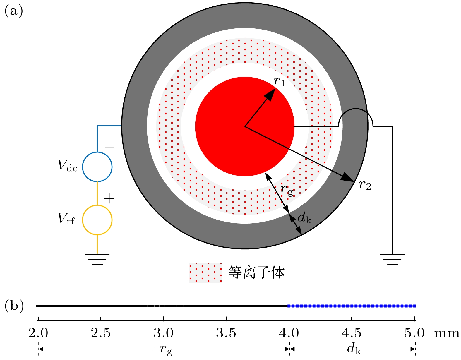
图 1 (a) 放电模型结构; (b) 径向网格剖分图
Fig. 1. (a) Structure diagram of discharge model; (b) radial meshing diagram.
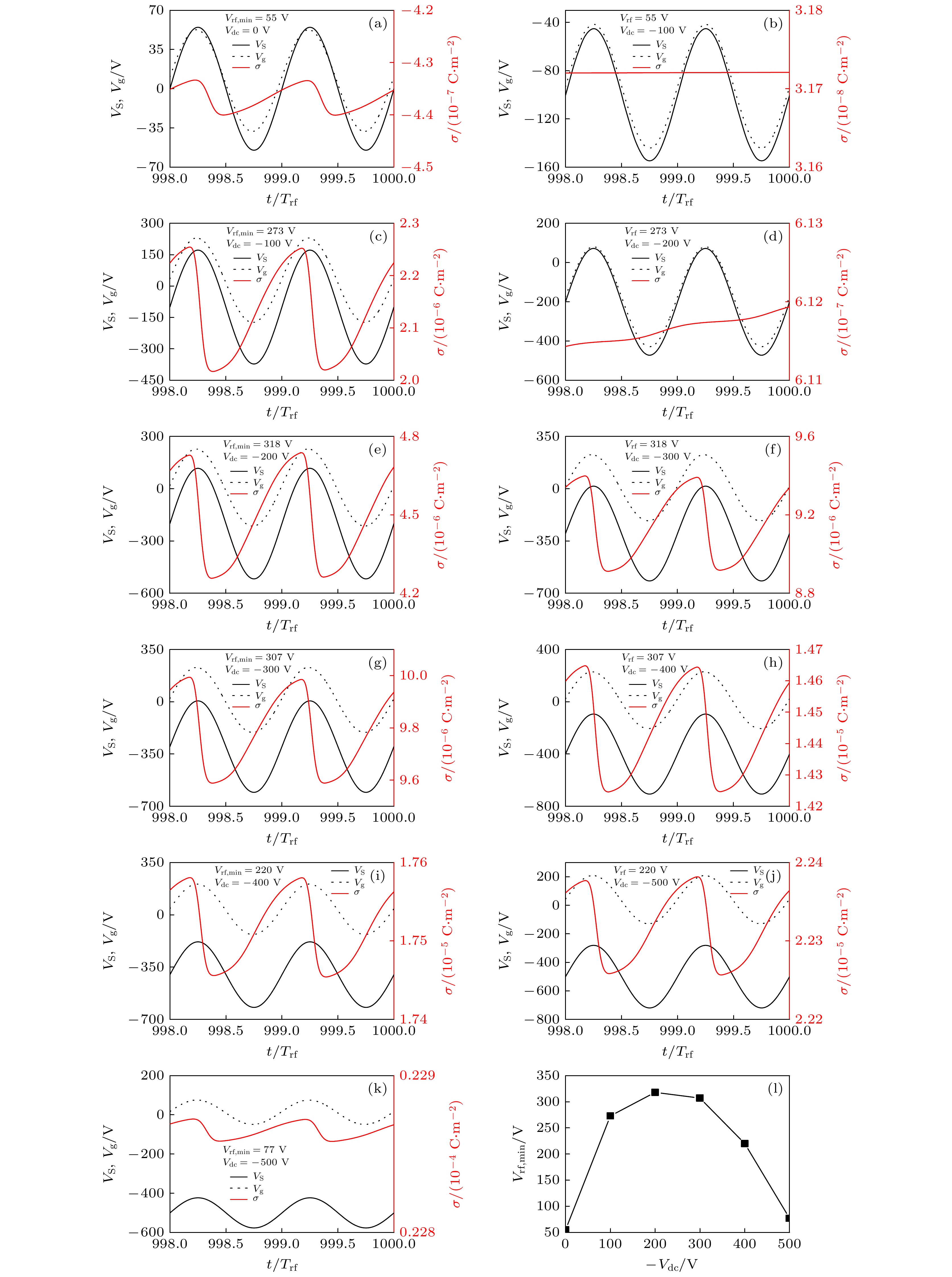
图 2 (a)—(k) DBD放电参数时域波形; (l) 射频最小维持放电电压振幅随直流电压的变化曲线
Fig. 2. (a)–(k) Time domain waveform of DBD discharge parameters; (l) variation of rf minimum sustaining discharge voltage amplitude with dc voltage.
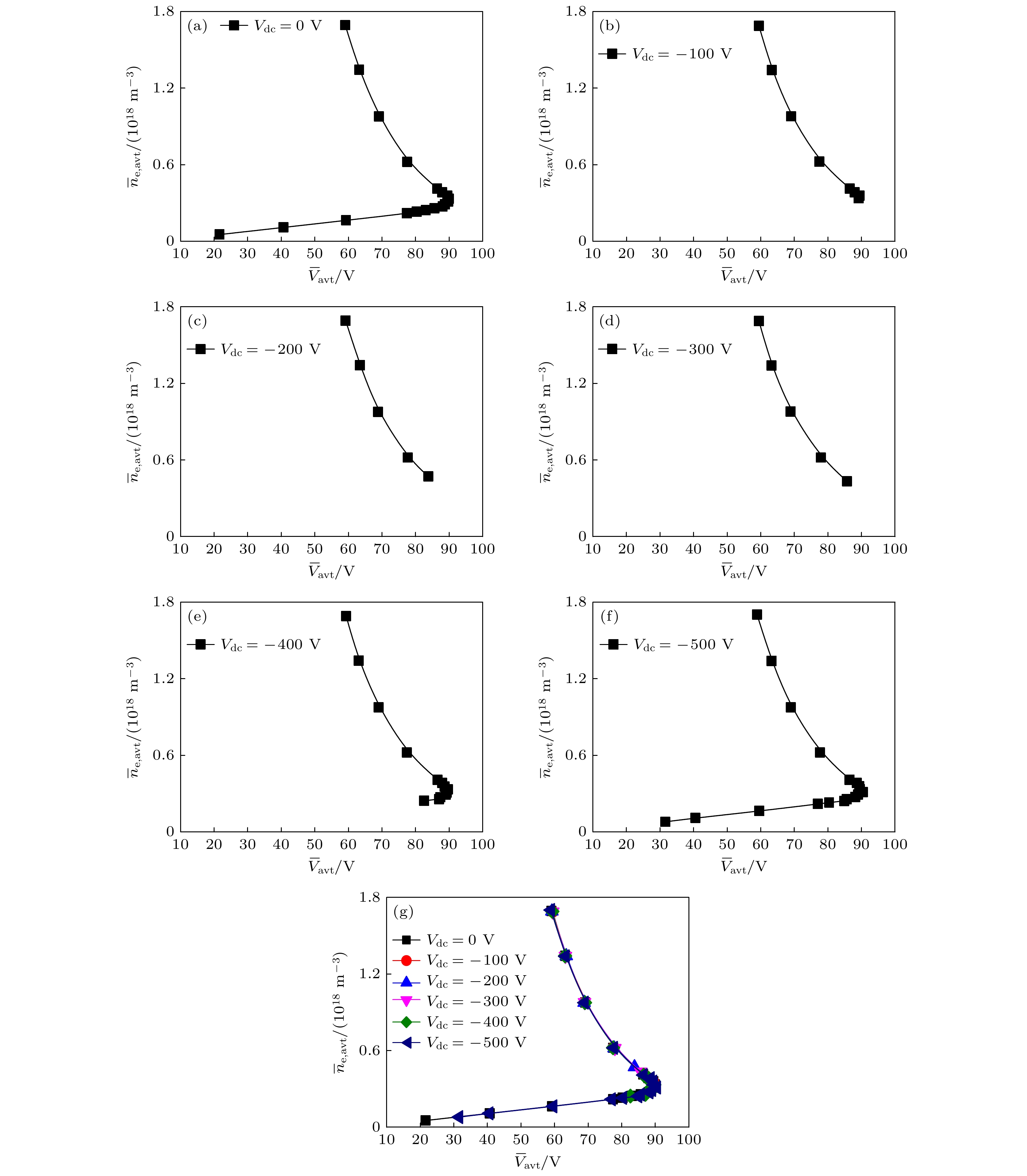
图 3 不同直流电压下, 周期平均电子密度平均值随周期平均气体电压平均值的变化 (a) 0 V; (b) –100 V; (c) –200 V; (d) –300 V; (e) –400 V; (f) –500 V; (g) 0— –500 V
Fig. 3. Average value of period average electron density varying with the average value of period average gas voltage with different voltage: (a) 0 V; (b) –100 V; (c) –200 V; (d) –300 V; (e) –400 V; (f) –500 V; (g) 0− –500 V.
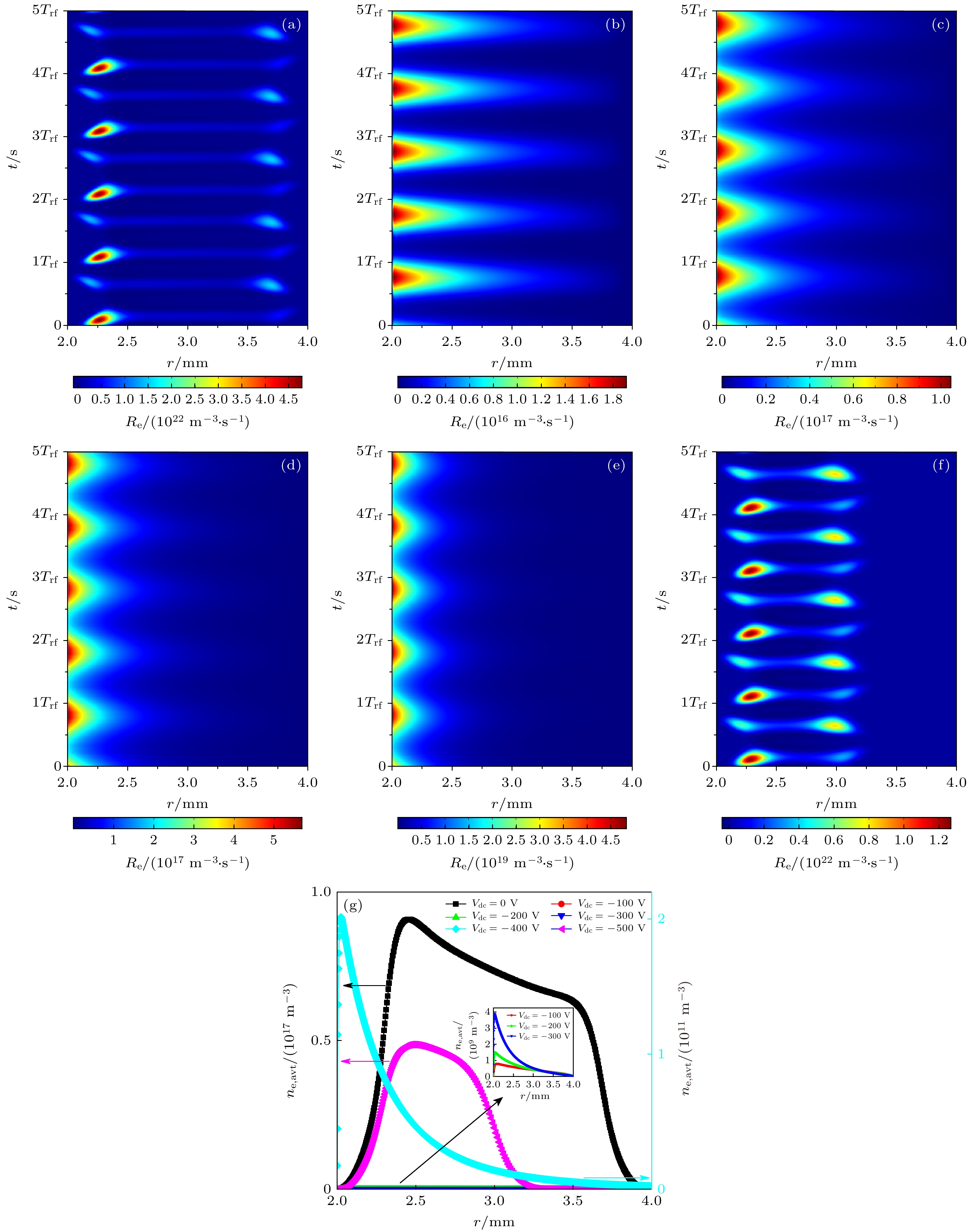
图 4 Vrf = 55 V条件下, 直流电压为(a) 0, (b) –100, (c) –200, (d) –300, (e) –400和(f) –500 V时, 电子产生率时空分布; (g) 周期平均电子密度径向分布
Fig. 4. Under the condition of Vrf = 55 V, spatial-temporal distribution of electron generation rate at different dc voltage of (a) 0, (b) –100, (c) –200, (d) –300, (e) –400 and (f) –500 V; (g) radial distribution of period average electron density.
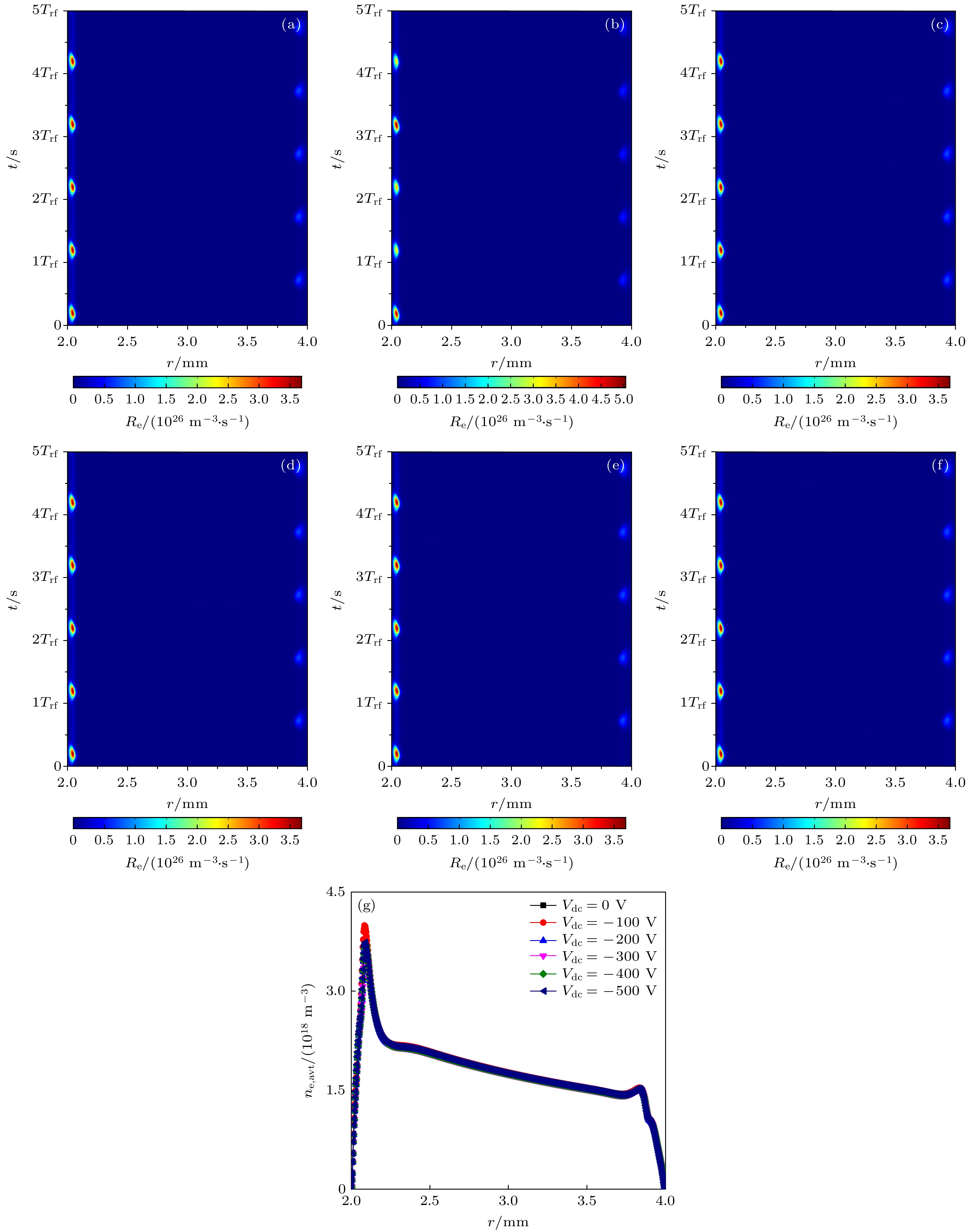
图 5 Vrf = 500 V条件下, 直流电压分别为(a) 0, (b) –100, (c) –200, (d) –300, (e) –400和(f) –500 V时, 电子产生率时空分布;(g) 周期平均电子密度径向分布
Fig. 5. Under the condition of Vrf = 500 V, spatial-temporal distribution of electron generation rate with dc voltage of (a) 0, (b) –100, (c) –200, (d) –300, (e) –400 and (f) –500 V; (g) radial distribution of period average electron density.
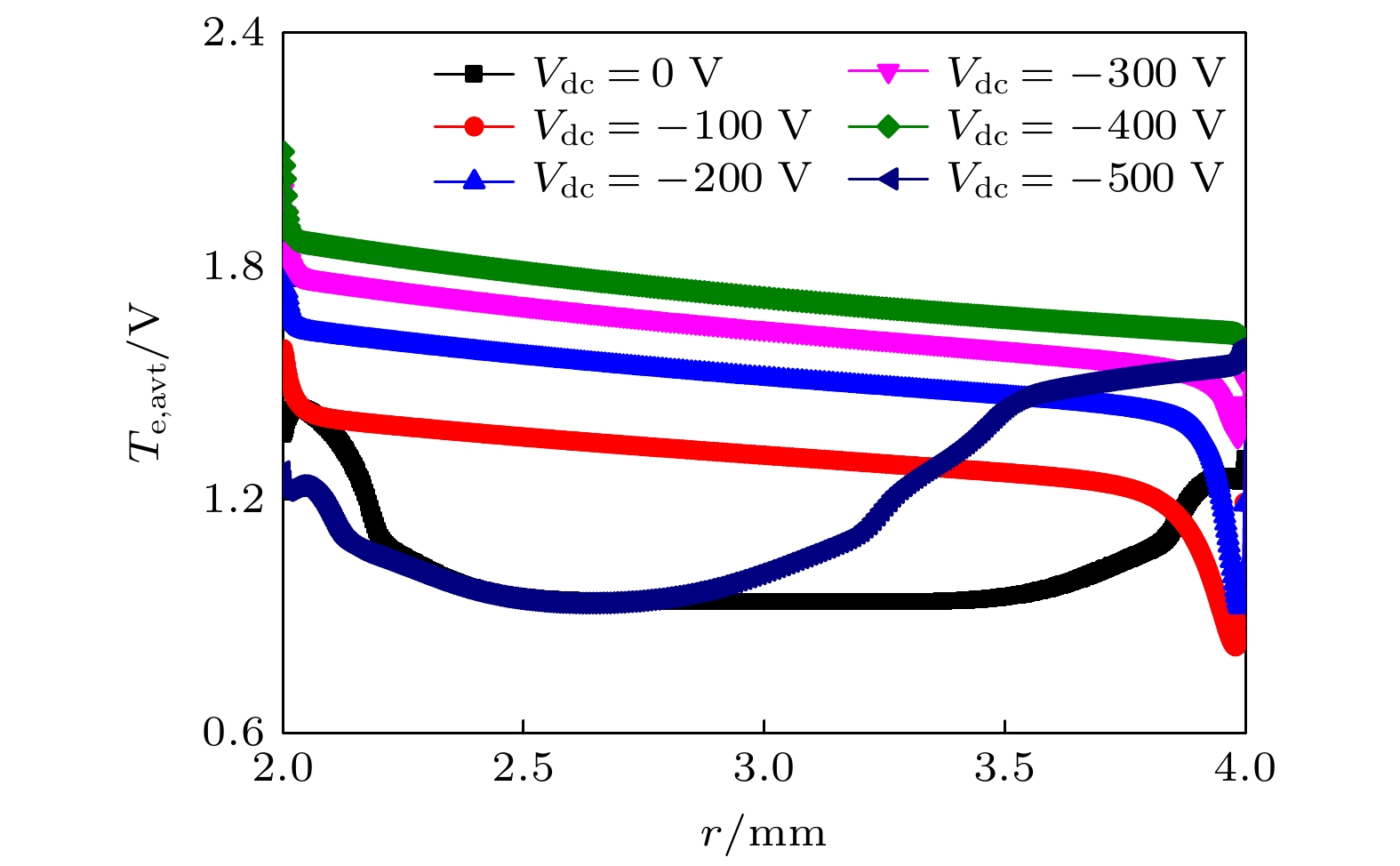
图 6 不同直流电压下, 周期平均电子温度径向分布(Vrf = 55 V)
Fig. 6. Radial distribution of the period average electron temperature with different dc voltages (Vrf = 55 V).
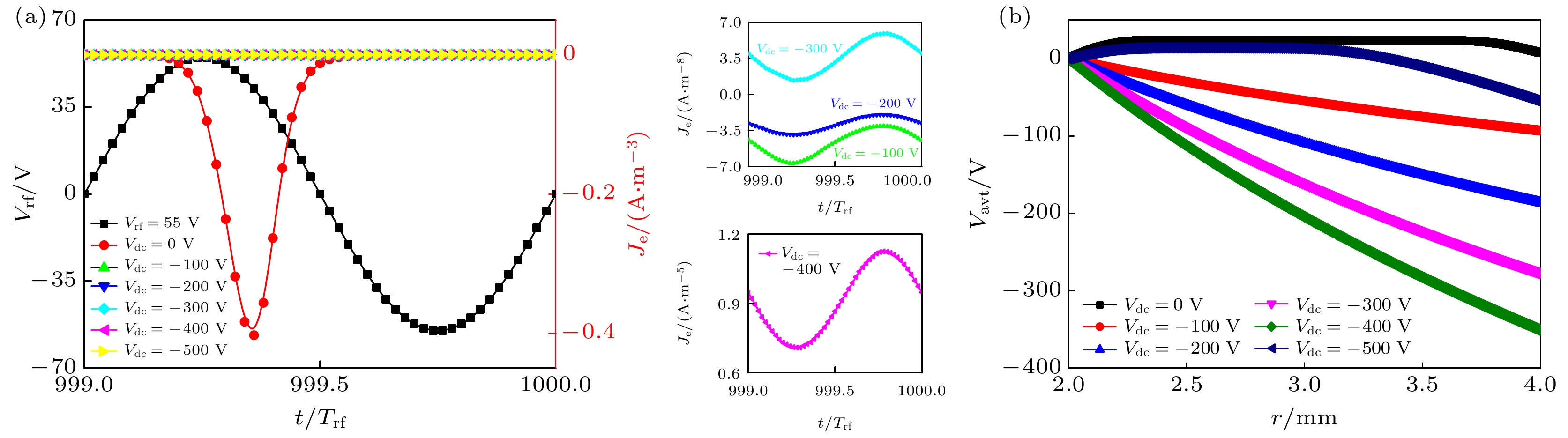
图 7 Vrf = 55 V时, 不同直流电压下, (a)流向介质表面的电子传导电流密度; (b) 周期平均气体电压径向分布
Fig. 7. Under different dc voltage and Vrf = 55 V, (a) electron conduction current density on dielectric surface; (b) radial distribution of period average gas voltage.
表 1 本文放电模型中所涉及的化学反应
Table 1. Chemical reaction formulas used in the discharge model.
反应方程 反应系数 ${\text{e + Ar} } \to {\text{2e + A} }{ {\text{r} }^{\text{ + } } }$ BOLSIG+ $ {\text{e + Ar}} \to {\text{e + A}}{{\text{r}}^{\text{*}}} $ BOLSIG+ ${\rm{e}} + {\rm{A}}{{\rm{r}}^*} \to 2 {\rm{e}} + {\rm{A}}{{\rm{r}}^ + }$ BOLSIG+ $2 {\rm{A}}{{\rm{r}}^*} \to {\rm{e}} + {\rm{A}}{{\rm{r}}^ + } + {\rm{Ar}}$ 1.2×10⁻⁹×NA cm3·s–1 ${\rm{A}}{{\rm{r}}^ + } + 2 {\rm{Ar}} \to {\rm{Ar}}_2^ + + {\rm{Ar}}$ 2.5×10⁻³¹×$ N_{\rm A}^2 $ cm6·s–1 ${\rm{e}} + {\rm{Ar}}_2^ + \to {\rm{A}}{{\rm{r}}^*} + {\rm{Ar}}$ 7×10–7×(300/Te×11600)1/2×NA
cm3·s–1${\rm{A} }{ {\rm{r} }^*} \to {\rm{Ar} } + {{h} }\nu$ 5×10⁵ s–1 ${\rm{e}} + {\rm{Ar}} \to {\rm{e}} + {\rm{Ar}}$ BOLSIG+  下载: 导出CSV
-
[1] 高书涵, 王绪成, 张远涛 2020 物理学报 69 115204
Google Scholar
Gao S H, Wang X C, Zhang Y T 2020 Acta Phys. Sin. 69 115204
Google Scholar
[2] Wang J, Lei B Y, Xu Y G, Wang Y S, Tang J, Zhao W, Duan Y X 2020 Phys. Plasmas 27 043501
Google Scholar
[3] Tang J, Duan Y X, Zhao W 2010 Appl. Phys. Lett. 96 191503
Google Scholar
[4] 孔德霖, 杨冰彦, 何锋, 韩若愚, 缪劲松, 宋廷鲁, 欧阳吉庭 2021 物理学报 70 095205
Google Scholar
Kong D L, Yang B Y, He F, Han R Y, Miao J S, Song Y L, Ouyang J T 2021 Acta Phys. Sin. 70 095205
Google Scholar
[5] Zhang S, Gao Y, Sun H, Bai H, Wang R X, Shao T 2018 J. Phys. D: Appl. Phys. 51 274005
Google Scholar
[6] Shao T, Liu F, Hai B, Ma Y F, Wang R X, Ren C Y 2017 IEEE Trans. Dielectr. Electr. Insul. 24 1557
Google Scholar
[7] Inglezakis V J, Amzebek A, Kuspangaliyeva B, Sarbassov Y, Balbayeva G, Yerkinova A, Poulopoulos S G 2018 Desalin. Water Treat. 112 218
Google Scholar
[8] Xiong Z, Lu X, Cao Y, Ning Q, Ostrikov, Lu Y, Zhou X, Liu J 2011 Appl. Phys. Lett. 99 253703
Google Scholar
[9] 万海容, 郝艳捧, 房强, 苏恒炜, 阳林, 李立浧 2020 物理学报 69 145203
Google Scholar
Wan H R, Hao Y P, Fang Q, Su H W, Yang L, Li L C 2020 Acta Phys. Sin. 69 145203
Google Scholar
[10] Kohler K, Coburn J W, Horne D E, Kay E, Keller J H 1985 J. Appl. Phys. 57 59
Google Scholar
[11] Tian X B, Li J, Tian L, Gong C Z, Yang S Q, Chu K 2011 Surf. Coat. Technol. 206 1016
Google Scholar
[12] Oyanagi Y, Hibino Y, Sawamoto N, Wakabayashi H, Ogura A 2020 Jpn. J. Appl. Phys. 59 065502
Google Scholar
[13] Li H X, Xu T, Chen J M, Zhou H D, Liu H W 2004 Appl. Surf. Sci. 227 364
Google Scholar
[14] 解艳凤, 施芸城, 黄晓江, 石建军, 郭颖 2013 真空科学与技术学报 33 893
Xie Y F, Shi Y C, Huang X J, Shi J J, Guo Y 2013 Chin. J. Vac. Sci. Technol. 33 893
[15] Zhang Q Z 2014 Ph. D. Dissertation (Dalian: Dalian University of Technology) (in Chinese)
[16] Diomede P, Longo S, Economou D J, Capitelli M 2012 J. Phys. D: Appl. Phys. 45 175204
Google Scholar
[17] Radmilović-Radjenović M, Radjenović B 2006 Plasma Sources Sci. Technol. 15 1
Google Scholar
[18] Kawamura E, Lieberman M A, Lichtenberg A J 2007 J. Vac. Sci. Technol. , A 25 1456
Google Scholar
[19] Wang S, Xu X, Wang Y N 2012 Plasma Sci. Technol. 14 32
Google Scholar
[20] Kawajiri K, Ramachandran K, Nishiyama H 2005 Int. J. Heat. Mass Transfer 48 183
Google Scholar
[21] 罗海云, 冉俊霞, 王新新 2012 高电压技术 38 1070
Luo H Y, Ran J X, Wang X X 2012 High Voltage Eng. 38 1070
[22] 张增辉, 邵先军, 张冠军, 李娅西, 彭兆裕 2012 物理学报 61 045205
Google Scholar
Zhang Z H, Shao X J, Zhang G J, Li Y X, Peng Z Y 2012 Acta Phys. Sin. 61 045205
Google Scholar
[23] 胡艳婷, 张钰如, 宋远红, 王友年 2018 物理学报 67 225203
Google Scholar
Hu Y T, Zhang Y R, Song Y H, Wang Y N 2018 Acta Phys. Sin. 67 225203
Google Scholar
[24] Balcon N, Hagelaar G J M, Boeuf J P 2008 IEEE Trans. Plasma Sci. 36 2782
Google Scholar
[25] Ballah Z, Khelfaoui F 2020 J. King. Saud. Univ. Sci. 32 620
Google Scholar
[26] Dyatko N A, Ionikh Y Z, Kochetov I V, Marinov D L, Meshchanov A V, Napartovich A P, Petrov F B, Starostin S A 2008 J. Phys. D: Appl. Phys. 41 055204
Google Scholar
[27] Hagelaar G J M, Pitchford L C 2005 Plasma Sources Sci. Technol. 14 722
Google Scholar
[28] Min B, Lee S H, Park H G 2000 J. Vac. Sci. Technol. A 18 349
Google Scholar
[29] Makabe T, Petrovic Z 2014 Plasma Electronics: Applications in Microelectronic Device Fabrication Second Edition (New York and London: Taylor & Francis Group) pp268–269
[30] Lisovsikiy V A, Kharchenko N D, Yegorenkov V D 2008 J. Phys. D: Appl. Phys. 41 125207
Google Scholar
[31] E E Kunhardt 2000 IEEE Trans. Plasma Sci. 28 189
Google Scholar
[32] Tarnev K, Pavlova R 2019 J. Plasma Phys. 85 905850201
Google Scholar
[33] Brenning N, Gudmundsson J T, Lundin D, Minea T, Raadu M A, Helmersson U 2016 Plasma Sources Sci. Technol. 25 065024
Google Scholar
[34] Lieberman M A, Lichtenberg A J 2005 Principles of Plasma Discharges and Materials Processing (New York: Wiley-Interscience Press) pp360–362
[35] Balcon N, Aanesland A, Boswell R W 2007 Plasma Sources Sci. Technol. 16 217
Google Scholar
[36] Wei J, Xiang X, Zhong L D, Wang Y N 2008 Phys. Plasmas 15 033502
Google Scholar


 下载:
下载:
计量
- 文章访问数: 6051
- PDF下载量: 83
- 被引次数: 0
