-
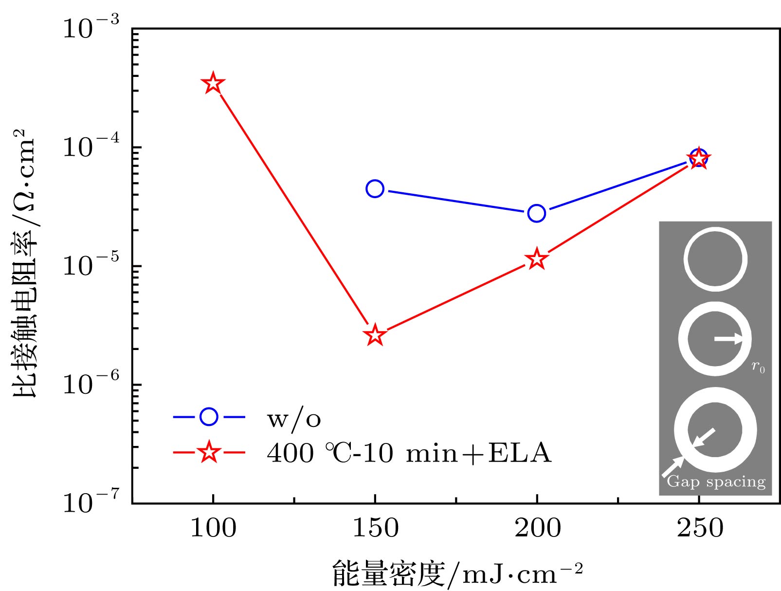
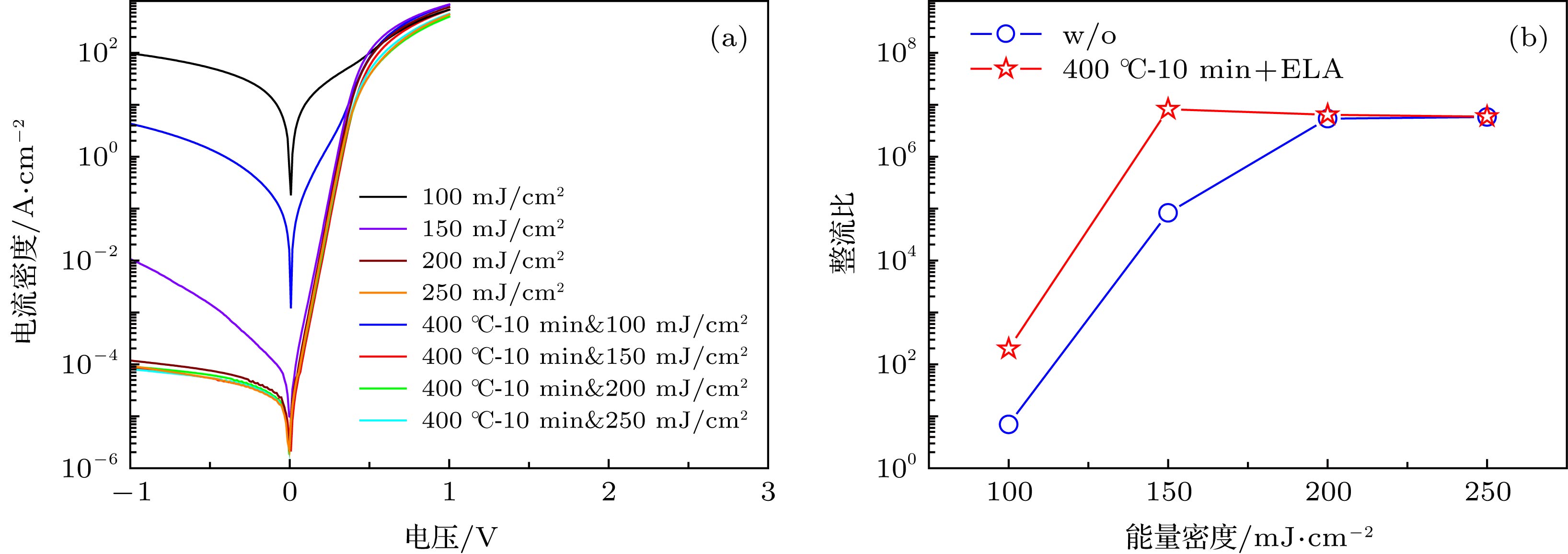
锗(Ge)中高激活浓度、低扩散深度的n型掺杂是实现高性能Ge n-MOSFET的重要前提条件. 本文采用低温预退火与脉冲激光退火相结合的两步退火法, 结合磷离子注入, 制备Al/n+Ge的欧姆接触以及Ge n+/p结二极管. 通过电流-电压特性测试来研究Al/n+Ge的欧姆接触以及Ge n+/p结二极管的性能, 测试结果表明: 低温预退火可初步修复注入损伤, 并降低激光退火时杂质的扩散深度; 结合离子注入工艺和两步退火工艺, Al/n+Ge欧姆接触的比接触电阻率降至2.61 × 10–6 Ω·cm2, Ge n+/p结二极管在 ± 1 V的整流比提高到8.35 × 10⁶, 欧姆接触及二极管性能均得到了显著提升.Silicon based germanium devices are crucial parts of optoelectronic integration as CMOS feature size continuously decreases. Germanium has attracted increasing attention due to its higher electron and hole mobility, larger optical absorption coefficient as well as lower processing temperature than those of silicon. However, the high diffusion coefficient and low solid solubility about n-type dopant and relatively high thermal budget required for high n-type doping in Ge make it difficult to achieve high activation n-type doping and excellent n+/p shallow junction for source/drain in the nano-scaled n-MOSFET (here MOSFET stands for). The high activation concentration and shallow junction n-type doping in Ge are greatly beneficial to the scaled Ge n-MOSFET technology. In this work, the ohmic contact of Al/n+Ge and Ge n+/p junction fabricated by a combination of low temperature pre-annealing process and excimer laser annealing for phosphorus-implanted germanium are demonstrated. Prior to excimer laser annealing, the samplesare annealed at a relatively low temperature, which can heal the implantation damages preliminarily. Through the optimization of pre-annealing temperature and time, the low temperature pre-annealing step can play a critical role in annihilating the implantation damages and significantly suppressing phosphorus diffusion in the laser annealing process, resulting in a very small dopant diffusion length at a high activation level of phosphorus. Through the combination of ion implantation and two-step annealing technology, the specific contact resistivity (ρC) of Al/n+Ge Ohmic contact is measured by CTLM structure. The optimized annealing condition is 400 oC-10 min of low temperature annealing and 150 mJ/cm2 of ELA. Under that annealing condition, the ρC of the sample by two-step annealing is reduced to 2.61 × 10⁻⁶ Ω·cm2, which is one order of magnitude lower than that by ELA alone (about 3.44 × 10⁻⁴ Ω·cm2). The lower value of ρC for the sample with LTPA can contribute to the higher carrier concentration and better crystalline quality thanthat without LTPA, which is confirmed by SRP and TEM. Moreover, the rectification ratio of Ge n+/p junction diode is improved to 8.35 × 10⁶ at ± 1 V, which is two orders of magnitudes higher than that by ELA alone. And a lower ideality factor of about 1.07 is also obtained than that by ELA alone, which indicates that the implantation damages can be repaired perfectly by two-step annealing method.
-
Keywords:
- low-temperature annealing /
- laser annealing /
- germanium /
- pn junction diode /
- Ohmic contact
[1] Chui C O, Ramanathan S, Triplett B, McIntyre P C, Saraswat K C 2002 IEEE Electron Device Lett. 23 473
 Google Scholar
[2] Park J H, Kuzum D, Jung W S, Saraswat K C 2011 IEEE Electron Device Lett. 32 234
 Google Scholar
[3] Zhang R, Huang P C, Lin J C, Taoka N, Takenaka M, Takagi S 2013 IEEE Trans. Electron Devices 60 927
 Google Scholar
[4] Morii K, Iwasaki T, Nakane R, Takenaka M, Takagi S 2010 IEEE Electron Device Lett. 31 1092
 Google Scholar
[5] Kuzum D, Krishnamohan T, Nainani A 2009 IEEE IEDM Tech. Dig. p1
[6] Martens K, Chui C O, Brammertz G, et al. 2008 IEEE Trans. Electron Devices 55 547
 Google Scholar
[7] Shang H, Frank M, Gusev E P, Chu J O, Bedell S W, Guarini K W, Ieong M 2006 IBM J. Res. Develop. 50 377
 Google Scholar
[8] Simoen E, Satta A, D’Amore A, et al. 2006 Mater. Sci. Semicond. Process 9 634
 Google Scholar
[9] Dimoulas A, Tsipas P, Sotiropoulos A 2006 Appl. Phys. Lett. 89 252110
 Google Scholar
[10] Kuzum D, Krishnamohan T, Nainani A, Sun Y, Pianetta P A, Wong H, Saraswat K C 2010 IEEE Trans. Electron Devices 58 59
[11] Chui C O, Kulig L, Moran J, Tsai W, Saraswa K 2005 Appl. Phys. Lett. 87 091909
 Google Scholar
[12] Wundisch C, Posselt M, Schmidt B, Heera V, Schumann T, Mucklich A, Grotzschel R, Skorupa W, Clarysse T, Simoen E, Hortenbach H 2009 Appl. Phys. Lett. 95 252107
 Google Scholar
[13] Zhang R, Li J, Chen F, Zhao Y 2016 IEEE Trans. Electron. Dev. 63 2665
 Google Scholar
[14] Yu B, Wang Y, Wang H, Xiang Q, Riccobene C, Talwar S, Lin M 1999 IEDM Tech. Dig. p509
[15] Wang C, Xu Y, Li C, Lin H 2018 Chin. Phys. B 27 018502
 Google Scholar
[16] Wang C, Li C, Huang S, et al. 2013 Appl. Phys. Exp. 6 106501
 Google Scholar
[17] Wang C, Li C, Lin G, et al. 2014 IEEE Trans. on Electron Dev. 61 3060
 Google Scholar
[18] Thareja G, Chopra S, Adamas B, Kim Y, Moffatt S, Saraswat K 2011 IEEE Electron Device Lett. 32 838
 Google Scholar
[19] Milazzo R, Napolitani E, Impellizzeri G, Fisicaro G, Boninelli S, Cuscuna M, de Salvador D, Mastromatteo M, Italia M, La Magna A 2014 J. Appl. Phys. 115 053501
 Google Scholar
[20] Tsouroutas P, Tsoukalas D, Florakis A, Zergioti I, Serafetinides A, Cherkashin N, Marty B, Claverie A 2006 Mater. Sci. Semicond. Processing 9 644
 Google Scholar
[21] Chao Y L, Woo J 2010 IEEE Trans. Electron Dev. 57 665
 Google Scholar
[22] Koike M, Kamata Y, Ino T, et al. 2008 J. Appl. Phys. 104 023523
 Google Scholar
[23] Ruan Y, Chen C, Huang S, Huang W, Chen S, Li C, Li J 2013 IEEE Trans. Electron Dev. 60 3741
 Google Scholar
-
表 1 不同退火条件下Ge n+/p结二极管的整流比和理想因子
Table 1. Rectification ratio and ideality factor of Ge n+/p junction diodes under different annealing conditions.
样品编号 退火条件 整流比(@ ± 1 V) 理想因子 R1 350 ℃-10 min&150 mJ/cm2 2 × 10⁵ 1.11 R2 400 ℃-10 min&150 mJ/cm2 8.35 × 10⁶ 1.08 R3 400 ℃-30 min&150 mJ/cm2 1.12 × 10² > 2 R4 450 ℃-10 min&150 mJ/cm2 13 > 2 -
[1] Chui C O, Ramanathan S, Triplett B, McIntyre P C, Saraswat K C 2002 IEEE Electron Device Lett. 23 473
 Google Scholar
[2] Park J H, Kuzum D, Jung W S, Saraswat K C 2011 IEEE Electron Device Lett. 32 234
 Google Scholar
[3] Zhang R, Huang P C, Lin J C, Taoka N, Takenaka M, Takagi S 2013 IEEE Trans. Electron Devices 60 927
 Google Scholar
[4] Morii K, Iwasaki T, Nakane R, Takenaka M, Takagi S 2010 IEEE Electron Device Lett. 31 1092
 Google Scholar
[5] Kuzum D, Krishnamohan T, Nainani A 2009 IEEE IEDM Tech. Dig. p1
[6] Martens K, Chui C O, Brammertz G, et al. 2008 IEEE Trans. Electron Devices 55 547
 Google Scholar
[7] Shang H, Frank M, Gusev E P, Chu J O, Bedell S W, Guarini K W, Ieong M 2006 IBM J. Res. Develop. 50 377
 Google Scholar
[8] Simoen E, Satta A, D’Amore A, et al. 2006 Mater. Sci. Semicond. Process 9 634
 Google Scholar
[9] Dimoulas A, Tsipas P, Sotiropoulos A 2006 Appl. Phys. Lett. 89 252110
 Google Scholar
[10] Kuzum D, Krishnamohan T, Nainani A, Sun Y, Pianetta P A, Wong H, Saraswat K C 2010 IEEE Trans. Electron Devices 58 59
[11] Chui C O, Kulig L, Moran J, Tsai W, Saraswa K 2005 Appl. Phys. Lett. 87 091909
 Google Scholar
[12] Wundisch C, Posselt M, Schmidt B, Heera V, Schumann T, Mucklich A, Grotzschel R, Skorupa W, Clarysse T, Simoen E, Hortenbach H 2009 Appl. Phys. Lett. 95 252107
 Google Scholar
[13] Zhang R, Li J, Chen F, Zhao Y 2016 IEEE Trans. Electron. Dev. 63 2665
 Google Scholar
[14] Yu B, Wang Y, Wang H, Xiang Q, Riccobene C, Talwar S, Lin M 1999 IEDM Tech. Dig. p509
[15] Wang C, Xu Y, Li C, Lin H 2018 Chin. Phys. B 27 018502
 Google Scholar
[16] Wang C, Li C, Huang S, et al. 2013 Appl. Phys. Exp. 6 106501
 Google Scholar
[17] Wang C, Li C, Lin G, et al. 2014 IEEE Trans. on Electron Dev. 61 3060
 Google Scholar
[18] Thareja G, Chopra S, Adamas B, Kim Y, Moffatt S, Saraswat K 2011 IEEE Electron Device Lett. 32 838
 Google Scholar
[19] Milazzo R, Napolitani E, Impellizzeri G, Fisicaro G, Boninelli S, Cuscuna M, de Salvador D, Mastromatteo M, Italia M, La Magna A 2014 J. Appl. Phys. 115 053501
 Google Scholar
[20] Tsouroutas P, Tsoukalas D, Florakis A, Zergioti I, Serafetinides A, Cherkashin N, Marty B, Claverie A 2006 Mater. Sci. Semicond. Processing 9 644
 Google Scholar
[21] Chao Y L, Woo J 2010 IEEE Trans. Electron Dev. 57 665
 Google Scholar
[22] Koike M, Kamata Y, Ino T, et al. 2008 J. Appl. Phys. 104 023523
 Google Scholar
[23] Ruan Y, Chen C, Huang S, Huang W, Chen S, Li C, Li J 2013 IEEE Trans. Electron Dev. 60 3741
 Google Scholar
计量
- 文章访问数: 20833
- PDF下载量: 107
- 被引次数: 0


 下载:
下载:


