-
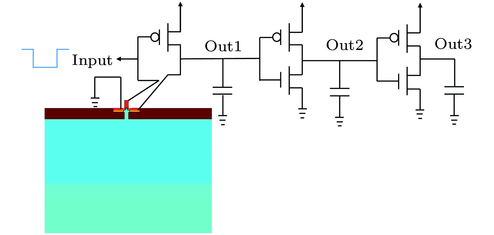
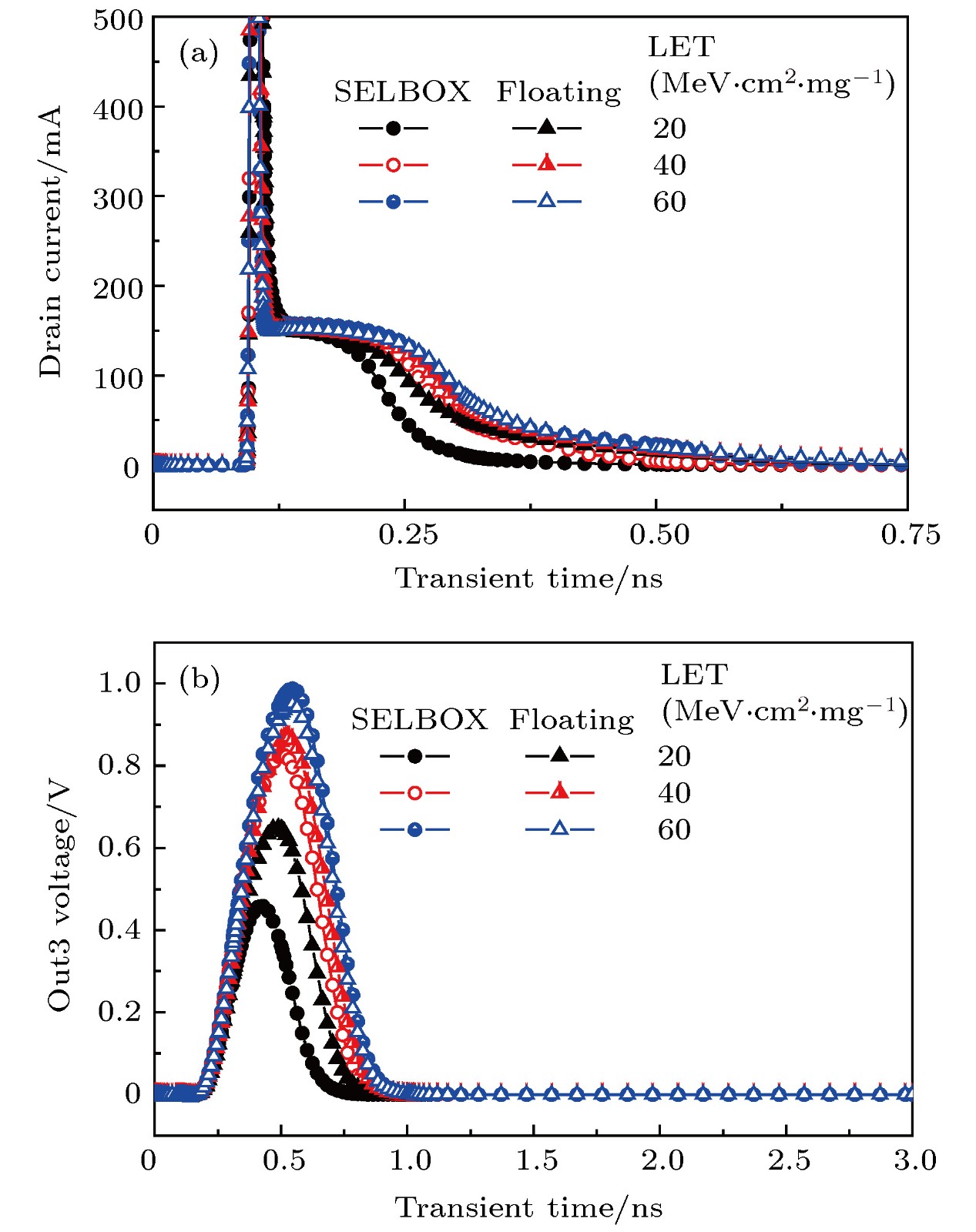
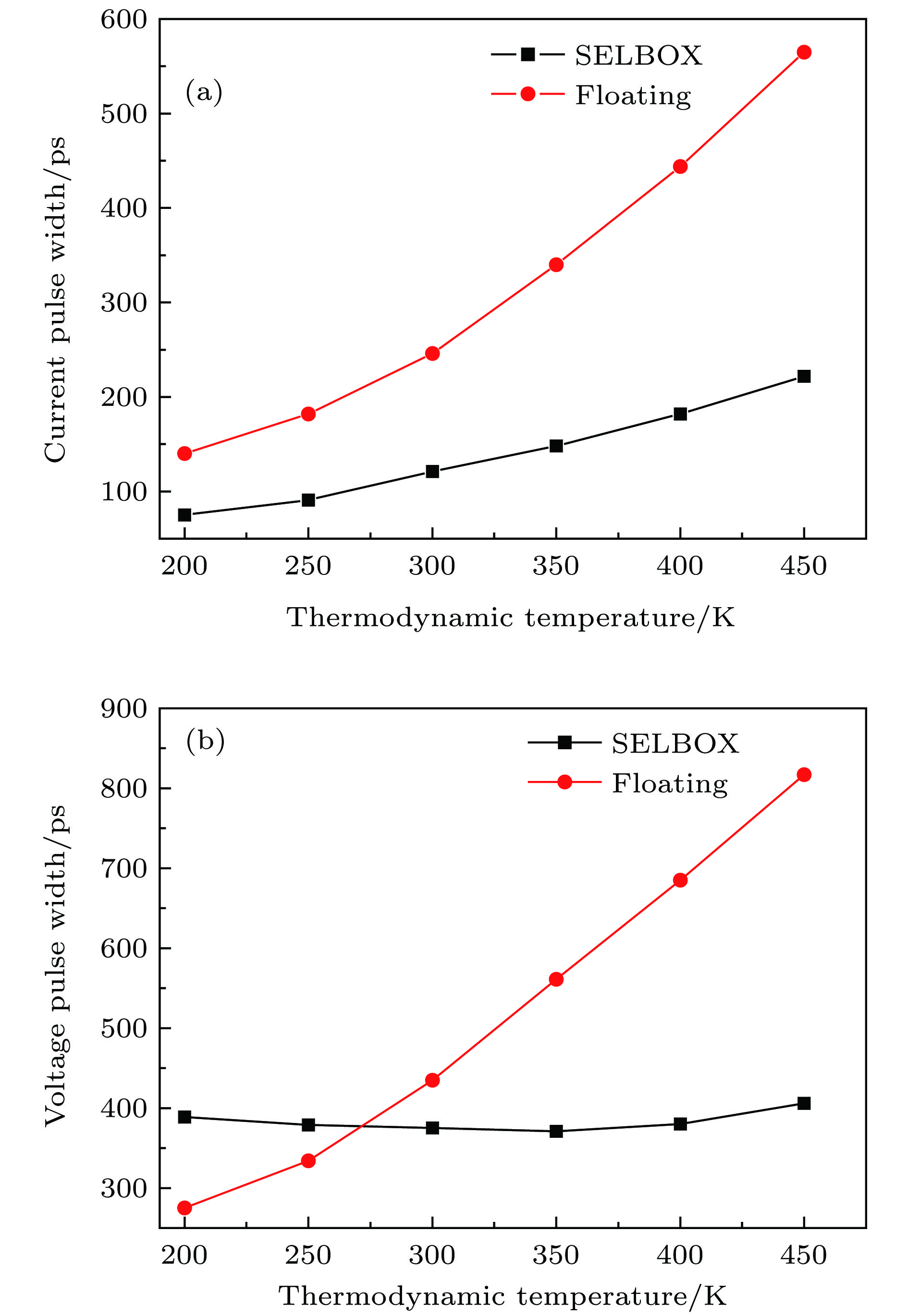
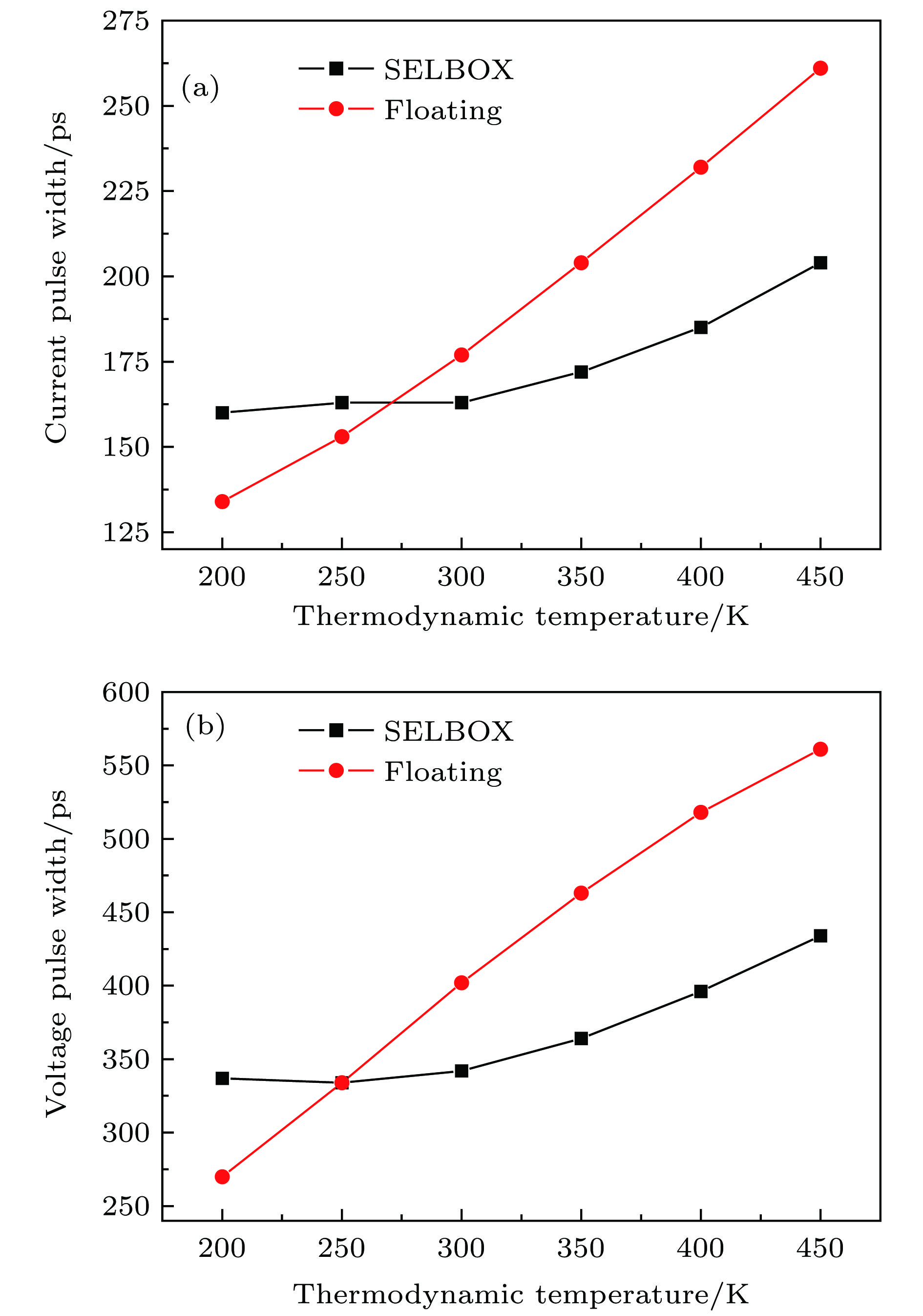
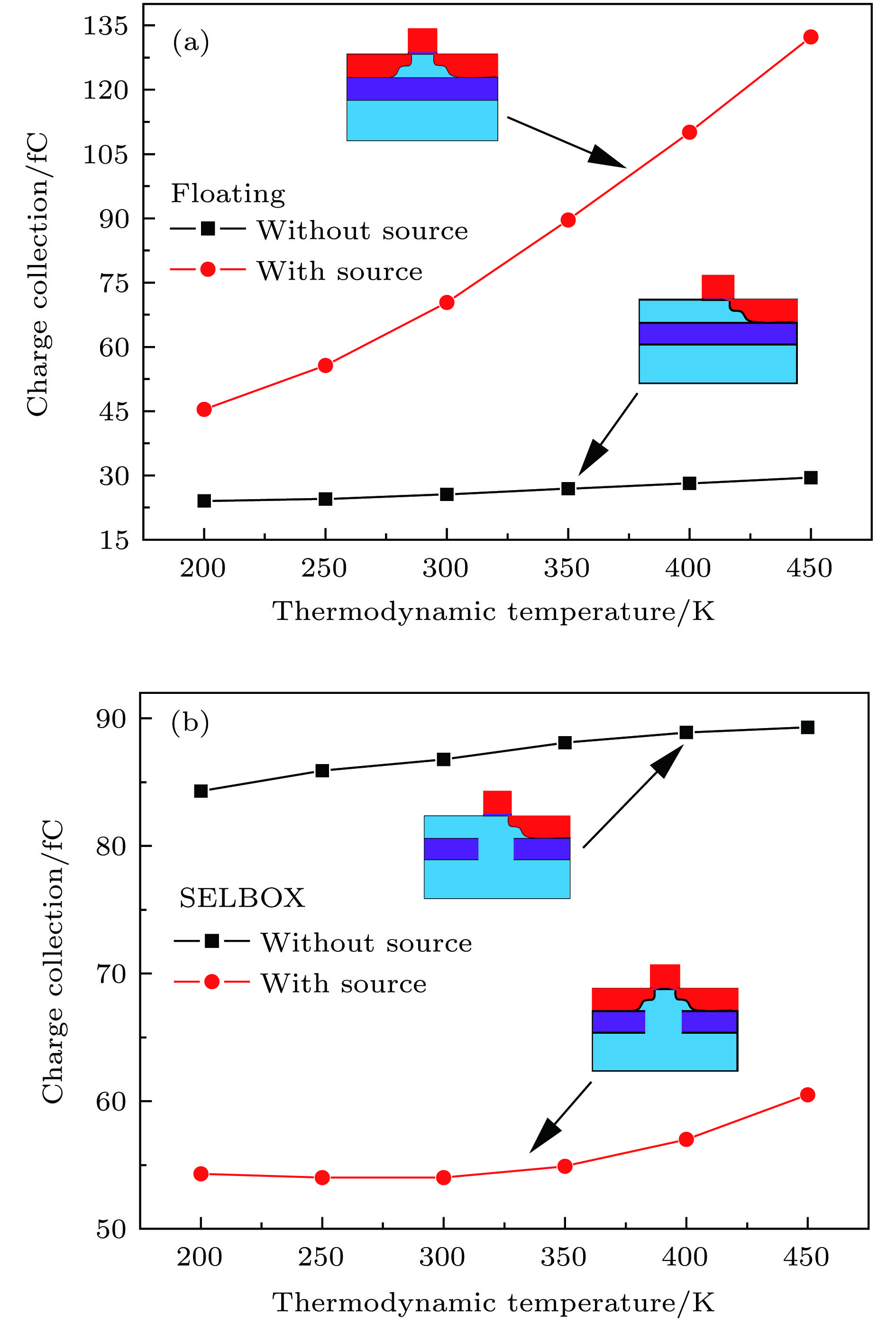
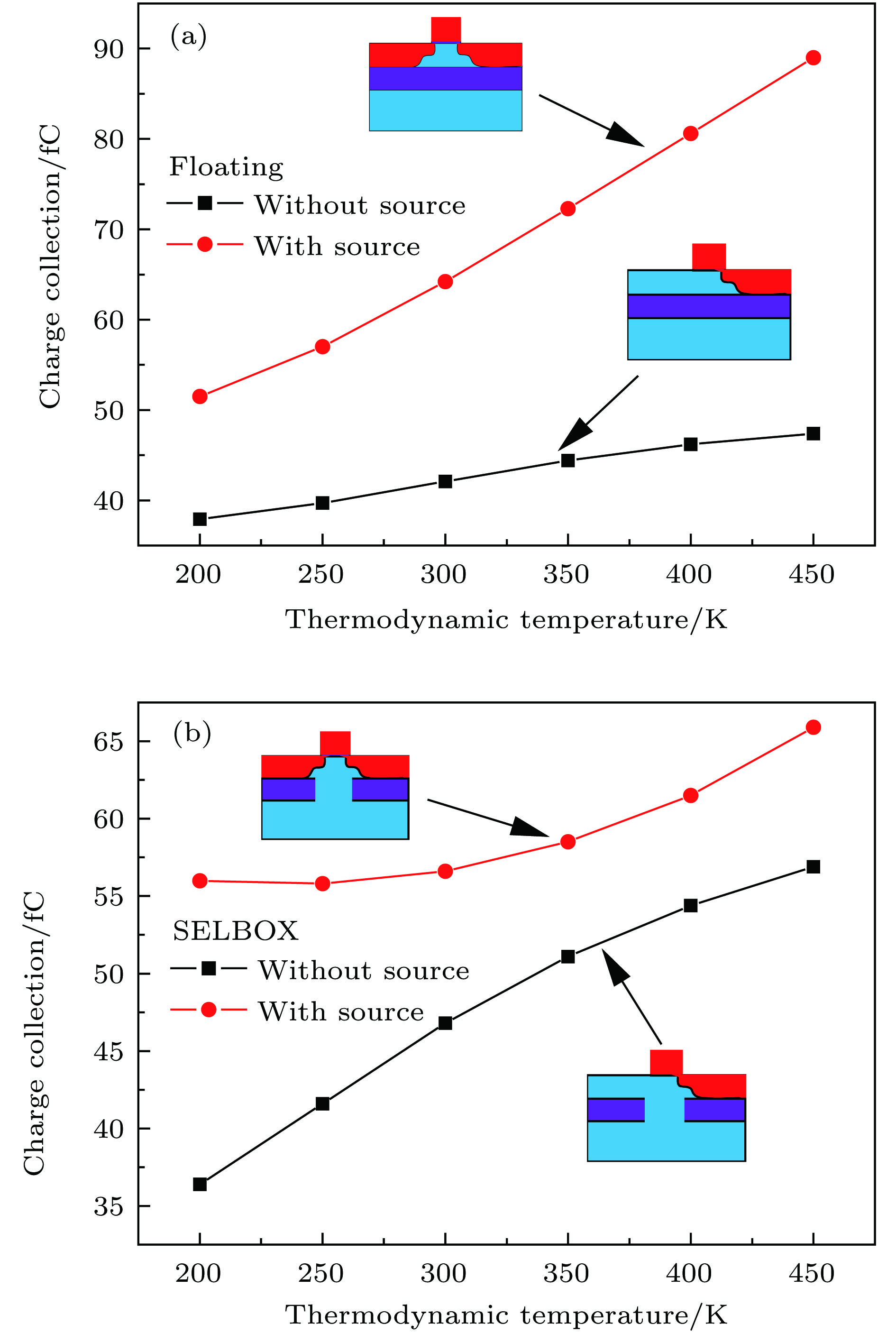
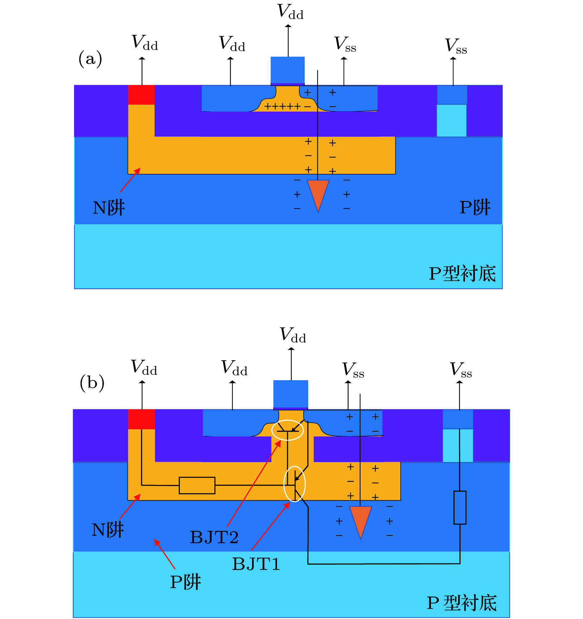
本文建立了90 nm工艺下的绝缘体上硅浮体器件和选择性埋氧层上硅器件模型, 通过器件电路混合仿真探究了工作温度对上述两种结构的多级反相器链单粒子瞬态脉冲宽度以及器件内部电荷收集过程的影响. 研究表明, N型选择性埋氧层上硅器件相较于浮体器件具有更好的抗单粒子能力, 但P型选择性埋氧层上硅器件的抗单粒子能力在高线性能量转移值下与浮体器件基本相同. 同时电荷收集的温度相关性分析表明, N型选择性埋氧层上硅器件只存在漂移扩散过程, 当温度升高时其电荷收集量变化很小, 而N型浮体器件存在双极放大过程, 电荷收集量随着温度的升高而显著增加; 另外, P型选择性埋氧层上硅器件和浮体器件均存在双极放大过程, 当温度升高时P型选择性埋氧层上硅器件衬底中的双极放大过程越来越严重, 由于局部埋氧层的存在, 反而抑制了其源极的双极放大过程, 导致它的电荷收集量要明显少于P型浮体器件. 因此选择性埋氧层上硅器件比浮体器件更好地抑制了温度对单粒子瞬态脉冲的影响.The silicon-on-insulator (SOI) device has been found to possess low leakage current and high operation speed due to reduced internal capacitances. The sensitive volume for charge collection in SOI device is smaller than that in bulk-silicon device, which improves the ability of SOI devices to resist single-event effect (SEE). In spite of these benefits, the SOI device has certain undesirable effects such as the kink effect. To mitigate the kink effect, selective-buried-oxide (SELBOX) SOI structure has been introduced. Space-borne electronic circuits based on SOI technology recently have been used in high radiation and extreme temperature environments. However, temperature affects internal carrier transport process and impact ionization process, which makes single-event transient (SET) pulse widths increased. Most of previous researches regarding temperature dependence of SEE were for SOI floating-body devices. But the influence of operating temperature on SEE of SELBOX SOI devices are yet unclear. In this paper, an SOI floating-body device and a SELBOX SOI device under 90 nm process are established by three-dimensional device simulation, and then temperature dependence of SET response in partially depleted SOI inverter chains is studied by a mixed-mode approach over a temperature range from 200 K to 450 K. Simulation results show that the N-type SELBOX SOI device has a better ability to resist SEE than the floating-body device, while the P-type SELBOX SOI device has the same ability to resist SEE at high linear energy transfer value as the floating-body device. And temperature dependence analysis of charge collection indicates that there is only drift-diffusion process in the N-type SELBOX SOI device. The amount of charge collection in the N-type SELBOX SOI device almost does not change with the increase of temperature. In addition, both the P-type SELBOX SOI device and the P-type floating-body device have a bipolar amplification process. With the increase of temperature, the bipolar amplification process in the substrate turns more serious. However, it suppresses the bipolar amplification process of the source because of SELBOX structure, so that the amount of charge collection is reduced in the drain significantly. According to our simulation results, compared with the floating-body device, the SELBOX SOI device can very well suppress the influence of temperature on SET pulse.
-
Keywords:
- selective buried oxide /
- single event transient /
- charge collection /
- temperature dependence
[1] 张正选, 邹世昌 2017 科学通报 62 1004
Zhang Z X, Zou S C 2017 Chin. Sci. Bull. 62 1004
[2] England T D, Arora R, Fleetwood Z F, Lourenco N E, Moen K A, Cardoso A S, McMorrow D, Roche N J H, Warner J H, Buchner S P, Paki P, Sutton A K, Freeman G, Cressler J D 2013 IEEE Trans. Nucl. Sci. 60 4405
 Google Scholar
[3] Dodd P E, Shaneyfelt A R, Horn K M, Walsh D S, Hash G L, Hill T A, Draper B L, Schwank J R, Sexton F W, Winokur P S 2002 IEEE Trans. Nucl. Sci. 48 1893
[4] Bartra W C, Vladimirescu A, Reis R 2015 IEEE International Conference on Electronics, Circuits, and Systems (ICECS) Cairo, Egypt, December 6—9, 2015 p133
[5] Gouker P M, Tyrrell B, D'Onofrio R, Wyatt P, Soares T, Hu W L, Chen C S, Schwank J R, Shaneyfelt M R, Blackmore E W, Delikat K, Nelson M, McMarr P, Hughes H, Ahlbin J R, Weeden-Wright S, Schrimpf R 2011 IEEE Trans. Nucl. Sci. 58 2845
 Google Scholar
[6] Thakral B, Bakshi G, Kushwaha A K, Manica 2014 International Conference on Reliability Optimization and Information Technology (ICROIT) Faridabad, India, Feburary 6—8, 2014 p487
[7] Pelella M M, Fossum J G, Suh D, Krishnan S, Jenkins K A 1995 IEEE International SOI Conference Proceedings Tucson, USA, October 3—5, 1995 p8
[8] Alvarado J, Kilchytska V, Boufouss E, Soto-Cruz B S, Flandre D 2012 IEEE Trans. Nucl. Sci. 59 943
 Google Scholar
[9] Narayanan M R, Nashash H A 2016 The 11th International Conference on Advanced Semiconductor Devices & Microsystems (ASDAM) Smolenice, Slovakia, November 13—16, 2016 p61
[10] Younis D, Madathumpadical N, Al-Nashash H 2017 The 7th International Conference on Modeling, Simulation, and Applied Optimization (ICMSAO) Sharjah, United Arab Emirates, April 4—6, 2017 p1
[11] Gadlage M J, Ahlbin J R, Ramachandran V, Gouker P, Dinkins A C, Bhuva B L, Narasimham B, Schrimpf R D, McCurdy M W, Alles M L, Reed R A, Mendenhall M H, Massengill L W, Shuler R L, McMorrow D 2009 IEEE Trans. Nucl. Sci. 56 3115
 Google Scholar
[12] 蔡莉, 刘建成, 覃英参, 李丽丽, 郭刚, 史淑廷, 吴振宇, 池雅庆, 惠宁, 范辉, 沈东军, 何安林 2018 原子能科学技术 52 4
Cai L, Liu J C, Qin Y C, Li L L, Guo G, Shi S T, Wu Z Y, Chi Y Q, Hui N, Fan H, Shen D J, He A L 2018 Atomic Energy Sci. Technol. 52 4
[13] Liu T, Liu J, Geng C, Zhang Z G, Zhao F Z, Tong T, Sun Y M, Su H, Yao H J, Gu S, Xi K, Luo J, Liu G, Han Z S, Hou M D 2013 European Conference on Radiation and ITS Effects on Components and Systems Oxford, UK, September 23—27, 2013 p1
[14] Boufouss E, Alvarado J, Flandre D 2010 International Conference on High Temperature Electronics (HiTEC 2010) Albuquerque, USA, May 11—13, 2010 p77
[15] Li D W, Qin J R, Chen S M 2013 Chin. Phys. B 22 586
[16] Nanoscale Integration and Modeling Group http://ptm.asu.edu/[2018-10-29]
[17] Synopsys Inc. https://www.synopsys.com/silicon/tcad.html[2018-10-29]
[18] Liu K J, Chang T C, Yang R Y, Chen C E, Ho S H, Tsai J Y, Hsieh T Y, Cheng O, Huang C T 2014 Thin Solid Films 572 39
 Google Scholar
[19] 刘必慰, 陈建军, 陈书明, 池雅庆 2012 物理学报 61 096102
 Google Scholar
Liu B W, Chen J J, Chen S M, Chi Y Q 2012 Acta Phys. Sin. 61 096102
 Google Scholar
[20] Liu J Q, Zhao Y F, Wang L, Zheng H C, Lei S, Li T D 2017 Proceedings of the 2017 2nd International Conference on Automation, Mechanical Control and Computational Engineering Beijing, China, March 25—26, 2017 p500
[21] 刘恩科, 朱秉升, 罗晋生 2011 半导体物理学 第7版 (北京: 电子工业出版社) 第97—100页
Liu E K, Zhu B S, Luo J S 2011 The Physics of Semiconductors 7th Edition (Beijing: Electronics Industry) pp97—100 (in Chinese)
[22] Ball D R, Alles M L, Kauppila J S, Harrington R C, Maharrey J A, Nsengiyumva P, Haeffner T D, Rowe J D, Sternberg A L, Zhang E X, Bhuva B L, Massengill L W 2018 IEEE Trans. Nucl. Sci. 65 326
 Google Scholar
[23] Chen S M, Liang B, Liu B, Liu Z 2008 IEEE Trans. Nucl. Sci. 55 2914
 Google Scholar
[24] 刘必慰, 陈书明, 梁斌 2009 半导体学报 30 54
Liu B W, Chen S M, Liang B 2009 J. Semicond. 30 54
-
表 1 SOI器件工艺参数
Table 1. Technologic parameters of SOI devices.
参数 数值 多晶硅厚度/$ {\text{μ}}{\rm m}$ 0.15 栅氧层厚度/nm 1.4 埋氧层厚度/$ {\text{μ}}{\rm m}$ 0.16 埋氧层镂空宽度/$ {\text{μ}}{\rm m}$ 0.09 N型衬底浓度/cm–3 1×10¹⁶ N阱/P阱浓度/cm–3 5×10¹⁷ 源/漏浓度/cm–3 2×10²⁰ 源/漏轻掺杂 (LDD) 浓度/cm–3 1×10¹⁹ 阈值电压掺杂浓度/cm–3 7.6×10¹⁸ 冠状 (Halo) 掺杂浓度/cm–3 2×10¹⁸ -
[1] 张正选, 邹世昌 2017 科学通报 62 1004
Zhang Z X, Zou S C 2017 Chin. Sci. Bull. 62 1004
[2] England T D, Arora R, Fleetwood Z F, Lourenco N E, Moen K A, Cardoso A S, McMorrow D, Roche N J H, Warner J H, Buchner S P, Paki P, Sutton A K, Freeman G, Cressler J D 2013 IEEE Trans. Nucl. Sci. 60 4405
 Google Scholar
[3] Dodd P E, Shaneyfelt A R, Horn K M, Walsh D S, Hash G L, Hill T A, Draper B L, Schwank J R, Sexton F W, Winokur P S 2002 IEEE Trans. Nucl. Sci. 48 1893
[4] Bartra W C, Vladimirescu A, Reis R 2015 IEEE International Conference on Electronics, Circuits, and Systems (ICECS) Cairo, Egypt, December 6—9, 2015 p133
[5] Gouker P M, Tyrrell B, D'Onofrio R, Wyatt P, Soares T, Hu W L, Chen C S, Schwank J R, Shaneyfelt M R, Blackmore E W, Delikat K, Nelson M, McMarr P, Hughes H, Ahlbin J R, Weeden-Wright S, Schrimpf R 2011 IEEE Trans. Nucl. Sci. 58 2845
 Google Scholar
[6] Thakral B, Bakshi G, Kushwaha A K, Manica 2014 International Conference on Reliability Optimization and Information Technology (ICROIT) Faridabad, India, Feburary 6—8, 2014 p487
[7] Pelella M M, Fossum J G, Suh D, Krishnan S, Jenkins K A 1995 IEEE International SOI Conference Proceedings Tucson, USA, October 3—5, 1995 p8
[8] Alvarado J, Kilchytska V, Boufouss E, Soto-Cruz B S, Flandre D 2012 IEEE Trans. Nucl. Sci. 59 943
 Google Scholar
[9] Narayanan M R, Nashash H A 2016 The 11th International Conference on Advanced Semiconductor Devices & Microsystems (ASDAM) Smolenice, Slovakia, November 13—16, 2016 p61
[10] Younis D, Madathumpadical N, Al-Nashash H 2017 The 7th International Conference on Modeling, Simulation, and Applied Optimization (ICMSAO) Sharjah, United Arab Emirates, April 4—6, 2017 p1
[11] Gadlage M J, Ahlbin J R, Ramachandran V, Gouker P, Dinkins A C, Bhuva B L, Narasimham B, Schrimpf R D, McCurdy M W, Alles M L, Reed R A, Mendenhall M H, Massengill L W, Shuler R L, McMorrow D 2009 IEEE Trans. Nucl. Sci. 56 3115
 Google Scholar
[12] 蔡莉, 刘建成, 覃英参, 李丽丽, 郭刚, 史淑廷, 吴振宇, 池雅庆, 惠宁, 范辉, 沈东军, 何安林 2018 原子能科学技术 52 4
Cai L, Liu J C, Qin Y C, Li L L, Guo G, Shi S T, Wu Z Y, Chi Y Q, Hui N, Fan H, Shen D J, He A L 2018 Atomic Energy Sci. Technol. 52 4
[13] Liu T, Liu J, Geng C, Zhang Z G, Zhao F Z, Tong T, Sun Y M, Su H, Yao H J, Gu S, Xi K, Luo J, Liu G, Han Z S, Hou M D 2013 European Conference on Radiation and ITS Effects on Components and Systems Oxford, UK, September 23—27, 2013 p1
[14] Boufouss E, Alvarado J, Flandre D 2010 International Conference on High Temperature Electronics (HiTEC 2010) Albuquerque, USA, May 11—13, 2010 p77
[15] Li D W, Qin J R, Chen S M 2013 Chin. Phys. B 22 586
[16] Nanoscale Integration and Modeling Group http://ptm.asu.edu/[2018-10-29]
[17] Synopsys Inc. https://www.synopsys.com/silicon/tcad.html[2018-10-29]
[18] Liu K J, Chang T C, Yang R Y, Chen C E, Ho S H, Tsai J Y, Hsieh T Y, Cheng O, Huang C T 2014 Thin Solid Films 572 39
 Google Scholar
[19] 刘必慰, 陈建军, 陈书明, 池雅庆 2012 物理学报 61 096102
 Google Scholar
Liu B W, Chen J J, Chen S M, Chi Y Q 2012 Acta Phys. Sin. 61 096102
 Google Scholar
[20] Liu J Q, Zhao Y F, Wang L, Zheng H C, Lei S, Li T D 2017 Proceedings of the 2017 2nd International Conference on Automation, Mechanical Control and Computational Engineering Beijing, China, March 25—26, 2017 p500
[21] 刘恩科, 朱秉升, 罗晋生 2011 半导体物理学 第7版 (北京: 电子工业出版社) 第97—100页
Liu E K, Zhu B S, Luo J S 2011 The Physics of Semiconductors 7th Edition (Beijing: Electronics Industry) pp97—100 (in Chinese)
[22] Ball D R, Alles M L, Kauppila J S, Harrington R C, Maharrey J A, Nsengiyumva P, Haeffner T D, Rowe J D, Sternberg A L, Zhang E X, Bhuva B L, Massengill L W 2018 IEEE Trans. Nucl. Sci. 65 326
 Google Scholar
[23] Chen S M, Liang B, Liu B, Liu Z 2008 IEEE Trans. Nucl. Sci. 55 2914
 Google Scholar
[24] 刘必慰, 陈书明, 梁斌 2009 半导体学报 30 54
Liu B W, Chen S M, Liang B 2009 J. Semicond. 30 54
计量
- 文章访问数: 10791
- PDF下载量: 74
- 被引次数: 0


 下载:
下载:
