-
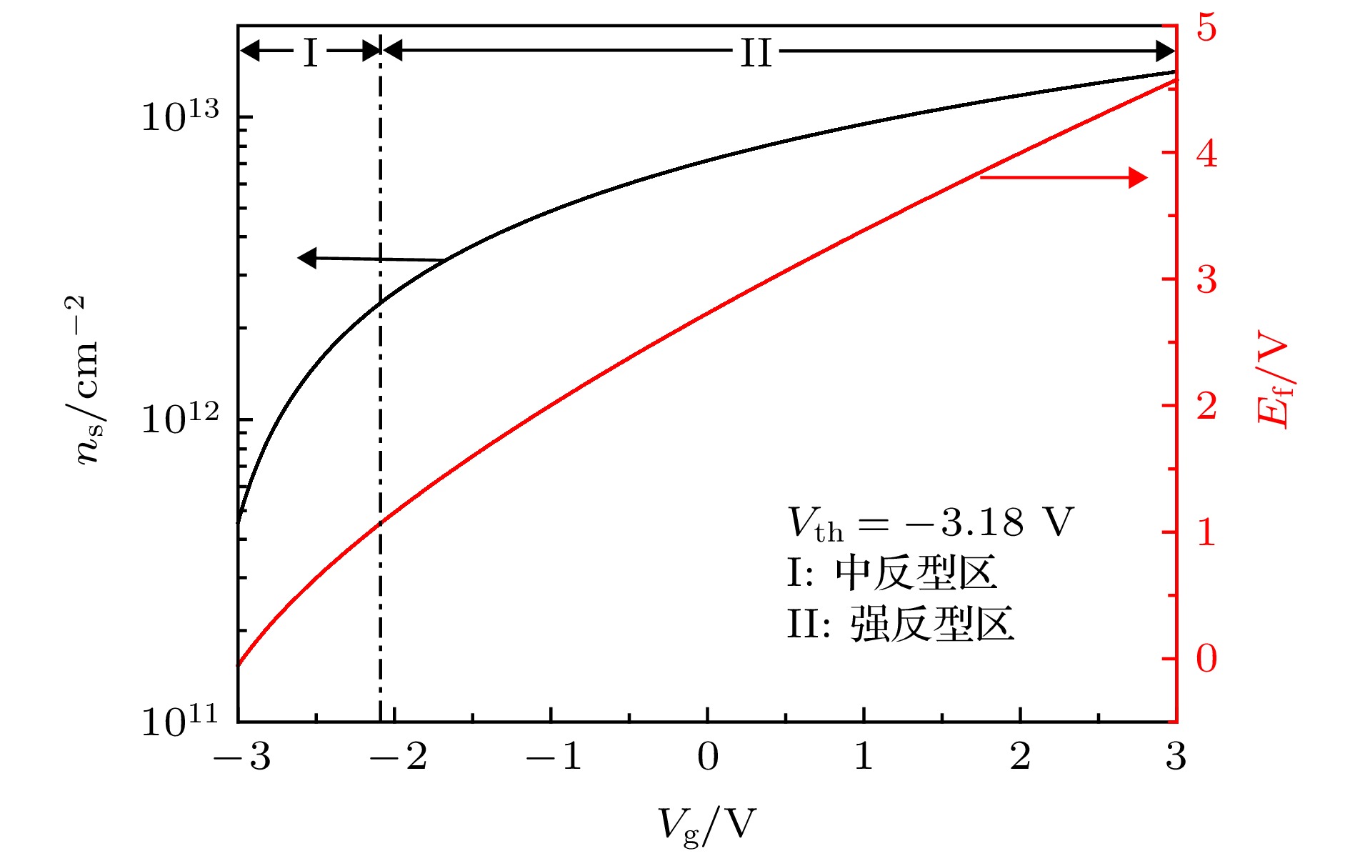
AlGaN/GaN HEMT外部边缘电容Cofd是由栅极垂直侧壁与二维电子气水平壁之间的电场构成的等效电容. 本文基于保角映射法对Cofd进行物理建模, 考虑沟道长度调制效应, 研究外部偏置、阈值电压漂移和温度变化对Cofd的影响: 随着漏源偏压从零开始增加, Cofd先保持不变再开始衰减, 其衰减速率随栅源偏压的增加而减缓; AlGaN势垒层中施主杂质浓度的减小和Al组分的减小都可引起阈值电压的正向漂移, 正向阈值漂移会加强沟道长度调制效应对Cofd的影响, 导致Cofd呈线性衰减. 在大漏极偏压工作情况下, Cofd对器件工作温度的变化更加敏感.
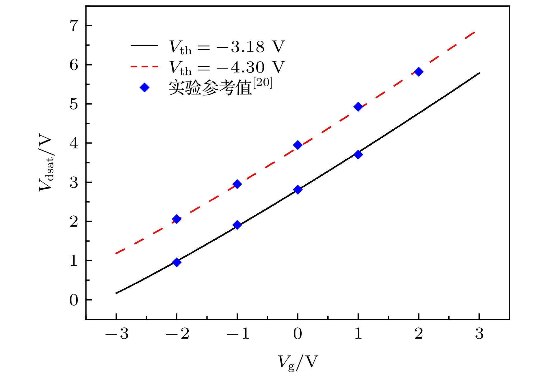
With the development of the application of AlGaN/GaN high electron mobility transistors in the radio frequency field, a capacitance model that can accurately describe the C-V characteristics of the device has become an important research topic. The gate capacitance of GaN HEMT can be divided into two parts: intrinsic capacitance and fringing capacitance related to two-dimensional electronic gas (2DEG) electrode. The fringing capacitance plays an important part in the switching device. The outer fringing capacitance Cofs/d dominates the fringing capacitance and is affected by the bias applied, especially the drain outer fringing capacitance Cofd. In order to establish the Cofd model which is related to the bias condition, the physics-based model of Cofd is established based on the conformal mapping, including the drain channel length variable. Since the drain channel length is related to the bias applied, the channel length modulation effect can be used to study how bias apllied effect the channel, and the relationship between Cofd and the bias condition is obtained. In addition, the threshold voltage variable is introduced when the channel length modulation effect is considered, and the threshold voltage drift caused by changes in the internal parameters and temperature of the device is studied using the threshold voltage variable in the model, and the relationship between Cofd and threshold voltage and temperature under different bias was obtained. It is found from the results of the study that as drain bias increases from zero, the channel length modulation effect keeps Cofd unchanged at lower drain bias. When the drain bias continues to increase, Cofd begins to decay again, and its decay rate slows down with the increase of gate bias. The decrease of donor impurity concentration and Al component in AlGaN barrier layer may increase the threshold voltage, which will strengthen the channel length modulation effect on Cofd, resulting in linear attenuation of Cofd. With the increasing of drain bias, the influence of threshold voltage shift on Cofd is enhanced, and the change of device operating temperature will enhance the threshold voltage shift and cause the deviation of Cofd. Moreover, with the continuous increase of drain bias, Cofd becomes more sensitive to the temperature variation. -
Keywords:
- HEMT /
- outer fringing capacitances /
- channel length modulation effect /
- model
[1] Jones E A, Wang F F, Costinett D 2016 IEEE J. Emerg. Sel. Top. Power Electron. 4 707
 Google Scholar
[2] 王林, 胡伟达, 陈效双, 陆卫 2010 物理学报 59 5730
 Google Scholar
Wang L, Hu W D, Chen X S, Lu W 2010 Acta Phys. Sin. 59 5730
 Google Scholar
[3] Zhang A, Zhang L, Tang Z, Cheng X, Wang Y, Chen K J, Chan M 2014 IEEE Trans. Electron Devices 61 755
 Google Scholar
[4] Pregaldiny F, Lallement C, Mathiot D 2002 Solid-State Electron. 46 2191
 Google Scholar
[5] Bansal A, Paul B C, Roy K 2005 IEEE Trans. Electron Devices 52 256
 Google Scholar
[6] Li K, Rakheja S 2018 Device Research Conference-Conference Digest, DRC the University of California, Santa Barbara, June 24–27, 2018 p1
[7] Jia Y, Xu Y, Wen Z, Wu Y, Guo Y 2019 IEEE Trans. Electron Devices 66 357
 Google Scholar
[8] Vetury R, Zhang N Q, Keller S, Mishra U K 2001 IEEE Trans. Electron Devices 48 560
 Google Scholar
[9] 郭伟玲, 陈艳芳, 李松宇, 雷亮, 柏常青 2017 发光学报 38 1000
Guo Y L, Chen Y F, Li S Y, Lei L, Bai C Q 2017 Chin. J. Lumin. 38 1000
[10] Cheng X, Wang Y 2011 IEEE Trans. Electron Devices 58 448
 Google Scholar
[11] Dasgupta N, DasGupta A 1993 Solid-State Electron. 36 201
 Google Scholar
[12] Huque M A, Eliza S A, Ragman T, Huq H F, Islam S K 2009 Solid-State Electron. 53 341
[13] Ahsan S A, Ghosh S, Sharma K, Dasgupta A, Khandelwal S, Chauhan Y S 2016 IEEE Trans. Electron Devices 63 565
[14] Rashmi, Kranti A, Haldar S, Gupta R S 2002 Solid-State Electron. 46 621
 Google Scholar
[15] Ambacher O, Smart J, Shealy J R, Weimann N G, Chu K, Murphy M, Schaff W J, Eastman L F, Dimitrov R, Wittmer L, Stutzmann M, Rieger W, Hilsenbeck J 1999 J. Appl. Phys 85 3222
 Google Scholar
[16] 范隆, 郝跃 2007 物理学报 56 3393
 Google Scholar
Fan L, Hao Y 2007 Acta Phys. Sin. 56 3393
 Google Scholar
[17] Ambacher O, Majewski J, Miskys C, Link A, Hermann M, Eickhoff M, Stutzmann M, Bernardini F, Fiorentini V, Tilak V, Schaff B, Eastman L F 2002 J. Phys.-Condes. Matter 14 3399
 Google Scholar
[18] Khandelwal S, Chauhan Y S, Fjeldly T A 2012 IEEE Trans. Electron Devices 59 2856
 Google Scholar
[19] He X G, Zhao D G, Jiang D S 2015 Chin. Phys. B 24 067301
 Google Scholar
[20] Li M, Wang Y 2008 IEEE Trans. Electron Devices 55 261
 Google Scholar
[21] Alim M A, Rezazadeh A A, Gaquiere C 2016 Semicond. Sci. Technol. 31 125016
 Google Scholar
-
表 1 模型仿真的器件参数值
Table 1. Model parameters in this paper.
参数 定义 数值 εx 有效介电常数 7.65ε0 Esat/V·μm–1 饱和电场 15 Ld/μm 漏端沟道长度 1 Tg/μm 栅极厚度 0.3 TAlGaN/nm AlGaN层厚度 22 $ E_{\rm g}^{\rm AIN} $/eV AIN禁带宽度 6.13 $ E_{\rm g}^{\rm GaN} $/eV GaN禁带宽度 3.42 Vtemp Vth的依赖系数温度 0.1689 TNOM/K 器件温标 300 ξ1 拟合参数 1.1 ξ2 拟合参数 0.24 m 拟合参数 1.2 p 拟合参数 0.307 τ 拟合参数 3.2 a 拟合参数 1.497 b 拟合参数 1.9 c 拟合参数 0.31 -
[1] Jones E A, Wang F F, Costinett D 2016 IEEE J. Emerg. Sel. Top. Power Electron. 4 707
 Google Scholar
[2] 王林, 胡伟达, 陈效双, 陆卫 2010 物理学报 59 5730
 Google Scholar
Wang L, Hu W D, Chen X S, Lu W 2010 Acta Phys. Sin. 59 5730
 Google Scholar
[3] Zhang A, Zhang L, Tang Z, Cheng X, Wang Y, Chen K J, Chan M 2014 IEEE Trans. Electron Devices 61 755
 Google Scholar
[4] Pregaldiny F, Lallement C, Mathiot D 2002 Solid-State Electron. 46 2191
 Google Scholar
[5] Bansal A, Paul B C, Roy K 2005 IEEE Trans. Electron Devices 52 256
 Google Scholar
[6] Li K, Rakheja S 2018 Device Research Conference-Conference Digest, DRC the University of California, Santa Barbara, June 24–27, 2018 p1
[7] Jia Y, Xu Y, Wen Z, Wu Y, Guo Y 2019 IEEE Trans. Electron Devices 66 357
 Google Scholar
[8] Vetury R, Zhang N Q, Keller S, Mishra U K 2001 IEEE Trans. Electron Devices 48 560
 Google Scholar
[9] 郭伟玲, 陈艳芳, 李松宇, 雷亮, 柏常青 2017 发光学报 38 1000
Guo Y L, Chen Y F, Li S Y, Lei L, Bai C Q 2017 Chin. J. Lumin. 38 1000
[10] Cheng X, Wang Y 2011 IEEE Trans. Electron Devices 58 448
 Google Scholar
[11] Dasgupta N, DasGupta A 1993 Solid-State Electron. 36 201
 Google Scholar
[12] Huque M A, Eliza S A, Ragman T, Huq H F, Islam S K 2009 Solid-State Electron. 53 341
[13] Ahsan S A, Ghosh S, Sharma K, Dasgupta A, Khandelwal S, Chauhan Y S 2016 IEEE Trans. Electron Devices 63 565
[14] Rashmi, Kranti A, Haldar S, Gupta R S 2002 Solid-State Electron. 46 621
 Google Scholar
[15] Ambacher O, Smart J, Shealy J R, Weimann N G, Chu K, Murphy M, Schaff W J, Eastman L F, Dimitrov R, Wittmer L, Stutzmann M, Rieger W, Hilsenbeck J 1999 J. Appl. Phys 85 3222
 Google Scholar
[16] 范隆, 郝跃 2007 物理学报 56 3393
 Google Scholar
Fan L, Hao Y 2007 Acta Phys. Sin. 56 3393
 Google Scholar
[17] Ambacher O, Majewski J, Miskys C, Link A, Hermann M, Eickhoff M, Stutzmann M, Bernardini F, Fiorentini V, Tilak V, Schaff B, Eastman L F 2002 J. Phys.-Condes. Matter 14 3399
 Google Scholar
[18] Khandelwal S, Chauhan Y S, Fjeldly T A 2012 IEEE Trans. Electron Devices 59 2856
 Google Scholar
[19] He X G, Zhao D G, Jiang D S 2015 Chin. Phys. B 24 067301
 Google Scholar
[20] Li M, Wang Y 2008 IEEE Trans. Electron Devices 55 261
 Google Scholar
[21] Alim M A, Rezazadeh A A, Gaquiere C 2016 Semicond. Sci. Technol. 31 125016
 Google Scholar
计量
- 文章访问数: 11700
- PDF下载量: 206
- 被引次数: 0


 下载:
下载:


