-
基于背散射抑制且对缺陷免疫的传输性质, 光子拓扑绝缘体为电磁传输调控提供了一种新颖的思路. 类比电子体系中的量子自旋霍尔效应, 本文设计出一种简单的二维介电光子晶体, 以实现自旋依赖的光子拓扑边界态. 该光子晶体是正三角环形硅柱子在空气中排列而成的蜂窝结构. 将硅柱子绕各自中心旋转60°, 可实现二重简并的偶极子态和四极子态之间的能带翻转. 这两对二重简并态的平均能流密度围绕原胞中心的手性可充当赝自旋自由度, 其点群对称性可用来构建赝时间反演对称. 根据
${{k}} \cdot {{p}}$ 微扰理论, 给出了布里渊区中心附近的有效哈密顿量以及对应的自旋陈数, 由此证实能带翻转的实质是拓扑相变. 数值计算结果揭示, 在拓扑非平庸和平庸的光子晶体分界面上可实现单向传输且对弯曲、空穴等缺陷免疫的拓扑边界态. 本文中的光子晶体只由电介质材料组成并且晶格结构简单, 实现拓扑相变时无需改变柱子的填充率或位置, 只需转动一个角度. 因此, 这种结构在拓扑边界态的应用中更为有效.Based on the transmission properties of against backscattering and robustness against defects, photonic topological insulators have opened up a novel way to steer the propagation of electromagnetic wave. In order to construct the photonic analogs of the quantum spin Hall effect in an electronic system, we propose a simple two-dimensional photonic crystal made of dielectric materials to realize topologically protected edge states associated with the photonic pseudospin. The photonic crystal comprises a honeycomb array of equilateral-triangle-ring-shaped silicon rods embedded in an air host. By simply rotating the silicon rods around their respective centers by 60°, the band inversion between a twofold degenerated dipolar mode and a twofold degenerated quadrupolar mode is clearly observed in the Brillouin zone center. For the double twofold degenerated states, the chirality of the time-averaged Poynting vector surrounding the unit cell center (i.e., right-hand or left-hand circular polarizations) plays the role of the pseudospin degree of freedom in the present photonic system, and their point group symmetry can be utilized to construct a pseudo-time-reversal symmetry. By utilizing${{k}} \cdot {{p}}$ perturbation theory, we develop an effective Hamiltonian for the associated dispersion relation around the Brillouin zone center and calculate the spin Chen number, which indicates that the band inversion leads to a topological phase transition from a trivial to a nontrivial state. With numerical simulations, we unambiguously demonstrate that the unidirectional propagation of pseudospin-dependent edge state along the interface between a topologically nontrivial photonic crystal and a trivial one, and robustness of the edge states against different defects including sharp bend and cavity, regardless of the type of interface. The photonic system proposed by us consists of dielectric materials and the corresponding lattice structure is simple. And without changing the fill ratio or changing the positions of the silicon rods, a simple rotation of the silicon rods can generate the topological phase transition. So the potential applications of the pseudospin-dependent edge states based on our design are expected in more efficient way.-
Keywords:
- photonic crystal /
- band inversion /
- topological phase transition /
- pseudospin
[1] Klitzing K V, Dorda G, Pepper M 1980 Phys. Rev. Lett. 45 494
 Google Scholar
[2] König M, Wiedmann S, Brüne C, Roth A, Buhmann H, Molenkamp L W, Qi X L, Zhang S C 2007 Science 318 766
 Google Scholar
[3] Kane C L, Mele E J 2005 Phys. Rev. Lett. 95 226801
 Google Scholar
[4] Bernevig B A, Hughes T L, Zhang S C 2006 Science 314 1757
 Google Scholar
[5] Hasan M Z, Kane C L 2010 Rev. Mod. Phys. 82 3045
 Google Scholar
[6] Qi X L, Zhang S C 2011 Rev. Mod. Phys. 83 1057
 Google Scholar
[7] Haldane F D, Raghu S 2008 Phys. Rev. Lett. 100 013904
 Google Scholar
[8] Wang Z, Chong Y D, Joannopoulos J D, Soljačić M 2008 Phys. Rev. Lett. 100 013905
 Google Scholar
[9] Wang Z, Chong Y, Joannopoulos J D, Soljačić M 2009 Nature 461 772
 Google Scholar
[10] Skirlo S A, Lu L, Igarashi Y, Yan Q, Joannopoulos J, Soljačić M 2015 Phys. Rev. Lett. 115 253901
 Google Scholar
[11] Skirlo S A, Lu L, Soljačić M 2014 Phys. Rev. Lett. 113 113904
 Google Scholar
[12] Minkov M, Savona V 2016 Optica 3 200
 Google Scholar
[13] Liu K, Shen L, He S 2012 Opt. Lett. 37 4110
 Google Scholar
[14] Khanikaev A B, Mousavi S H, Tse W K, Kargarian M, MacDonald A H, Shvets G 2013 Nat. Mater. 12 233
 Google Scholar
[15] Chen W J, Jiang S J, Chen X D, Zhu B, Zhou L, Dong J W, Chan C T 2014 Nat. Commun. 5 5782
 Google Scholar
[16] He C, Sun X C, Liu X P, Lu M H, Chen Y, Feng L, Chen Y F 2016 Proc. Natl. Acad. Sci. USA 113 4924
 Google Scholar
[17] Hafezi M, Demler E A, Lukin M D, Taylor J M 2011 Nat. Phys. 7 907
 Google Scholar
[18] Fang K, Yu Z, Fan S 2012 Nat. Photonics 6 782
 Google Scholar
[19] Rechtsman M C, Zeuner J M, Plotnik Y, Lumer Y, Podolsky D, Dreisow F, Nolte S, Segev M, Szameit A 2013 Nature 496 196
 Google Scholar
[20] Lu L, Gao H, Wang Z 2018 Nat. Commun. 9 5384
 Google Scholar
[21] Lu L, Fang C, Fu L, Johnson S G, Joannopoulos J D, Soljačić M 2016 Nat. Phys. 12 337
 Google Scholar
[22] Yang Y, Gao Z, Xue H, Zhang L, He M, Yang Z, Singh R, Chong Y, Zhang B, Chen H 2019 Nature 565 622
 Google Scholar
[23] Wu L H, Hu X 2015 Phys. Rev. Lett. 114 223901
 Google Scholar
[24] Yang Y, Xu Y F, Xu T, Wang H X, Jiang J H, Hu X, Hang Z H 2018 Phys. Rev. Lett. 120 217401
 Google Scholar
[25] Zhu X, Wang H X, Xu C, Lai Y, Jiang J H, John S 2018 Phys. Rev. B 97 085148
 Google Scholar
[26] Chen Z G, Mei J, Sun X C, Zhang X, Zhao J, Wu Y 2017 Phys. Rev. A 95 043827
 Google Scholar
[27] Chen X D, Deng W M, Lu J C, Dong J W 2018 Phys. Rev. B 97 184201
 Google Scholar
[28] Kang Y, Ni X, Cheng X, Khanikaev A B, Genack A Z 2018 Nat. Commun. 9 3029
 Google Scholar
[29] Khanikaev A B, Fleury R, Mousavi S H, Alù A 2015 Nat. Commun. 6 8260
 Google Scholar
[30] Zhang Z, Tian Y, Cheng Y, Wei Q, Liu X, Christensen J 2018 Phys. Rev. Appl. 9 034032
 Google Scholar
[31] Wei Q, Tian Y, Zuo S Y, Cheng Y, Liu X J 2017 Phys. Rev. B 95 094305
 Google Scholar
[32] He H, Qiu C, Ye L, Cai X, Fan X, Ke M, Zhang F, Liu Z 2018 Nature 560 61
 Google Scholar
[33] Zhang Z, Tian Y, Cheng Y, Liu X, Christensen J 2017 Phys. Rev. B 96 241306
 Google Scholar
[34] Mei J, Chen Z, Wu Y 2016 Sci. Rep. 6 32752
 Google Scholar
[35] Neto A H C, Guinea F, Peres N M R, Novoselov K S, Geim A K 2009 Rev. Mod. Phys. 81 109
 Google Scholar
[36] Mei J, Wu Y, Chan C T, Zhang Z Q 2012 Phys. Rev. B 86 035141
 Google Scholar
[37] Li Y, Wu Y, Chen X, Mei J 2013 Opt. Express 21 7699
 Google Scholar
[38] Shen S Q, Shan W Y, Lu H Z 2011 Spin 1 33
 Google Scholar
-
图 1 二维光子晶体的蜂窝结构示意图 (a) 由两个正三角环形硅柱子所组成的“人工原子”(图中用紫色标记)在空气中排列而成的三角晶格结构; (b) 与(a)相同, 但组成“人工原子”的两个硅柱子绕各自中心转动60°(图中用橙色标记). a为晶格常数,
${{{a}}_1}$ 和${{{a}}_2}$ 为晶格基矢, 硅柱的相对介电常数${\varepsilon _{\rm{r}}} = 12$ 和相对磁导率${\mu _{\rm{r}}} = 1$ , 内外正三角形的顶点到硅柱中心的距离分别为${r_1} = {0.2 a} / {\sqrt 3 }$ 和${r_2} = {0.45 a} /$ ${\sqrt 3 } $ , 相邻硅柱中心的相对距离为$L = {a / {\sqrt 3 }}$ , 红色正六边形所标记的区域表示三角晶格的原胞Fig. 1. Schematics of the honeycomb structure of two-dimensional photonic crystals: (a) Triangular lattice structure of “artificial atoms” composed by two equilateral-triangle-ring-shaped silicon rods, which are labeled by purple in the figure, embedded in an air host; (b) the same as pa-nel (a), except that the silicon rods are rotated by 60° around their respective centers, the corresponding “arti-ficial atom” is labeled by orange in the figure.
${{{a}}_1}$ and${{{a}}_2}$ are unit vectors with length a as the lattice constant. The relative permittivity and permeability of silicon rods are${\varepsilon _{\rm{r}}} = 12$ and${\mu _{\rm{r}}} = 1$ , respectively. The distance from the vertices of the inner and outer equilateral triangles to the center of the silicon rod are${r_1} = {{0.2 a} / {\sqrt 3 }}$ and$ {r_2} = $ $ {{0.45 a} / {\sqrt 3 }}$ , respectively. The distance between the centers of the neighboring silicon rods is$L = {a / {\sqrt 3 }}$ . Red hexagons represent the unit cells of the triangular lattices.图 2 能带结构与不可约表示
${E_1}$ 和${E_2}$ 所对应的本征态 (a) P型光子晶体的带结构; (b) N型光子晶体的带结构. (a), (b)中的插图给出Γ点的二重简并偶极子态(图中标记为${{\rm{p}}_x}/{{\rm{p}}_y}$ )和二重简并四极子态 (图中标记为${{\rm{d}}_{{x^2} - {y^2}}}/{{\rm{d}}_{xy}}$ )的磁场分布, 深红色和深蓝色分别表示磁场${H_z}$ 的正负最大值, 旋转硅柱子后发生了能带翻转; (c) P型光子晶体中偶极子态的平均能流密度分布; (d) P型光子晶体中四极子态的平均能流密度分布, 箭头显示能流密度的大小和方向. 在原胞中心附近, 能流密度具有逆时针和顺时针圆偏振特性, 反映出赝自旋向上和赝自旋向下的取向性Fig. 2. Band structures and the eigenstates for
${E_1}$ and${E_2}$ irreducible representations: (a) Band structure of P-type photonic cry-stal; (b) band structure of N-type photonic crystal, the insets of (a) and (b) show the magnetic field distributions of the twofold degenerated dipolar state (marked as${{\rm{p}}_x}/{{\rm{p}}_y}$ ) and the twofold degenerated quadrupolar state (marked as${{\rm{d}}_{{x^2} - {y^2}}}/{{\rm{d}}_{xy}}$ ) at Γ point, and the positive and negative maxima of the magnetic field,${H_z}$ , are represented by dark red and dark blue, respectively, band inversion takes place under the rotation of the silicon rods; (c) real-space distributions of the time-averaged Poynting vector for the dipolar states in P-type photonic crystal; (d) real-space distributions of the time-averaged Poynting vector for quadrupolar states in P-type photonic crystal; the arrows show the direction and magnitude of the Poynting vector, whose anticlockwise/clockwise circular polarization around the unit cell center reveals the pseudospin-up/pseudospin-down orientation.图 3 投影带结构与拓扑边界态 (a) 由拓扑非平庸和拓扑平庸光子晶体所组成的条带形的超原胞结构示意图; (b) 超原胞沿
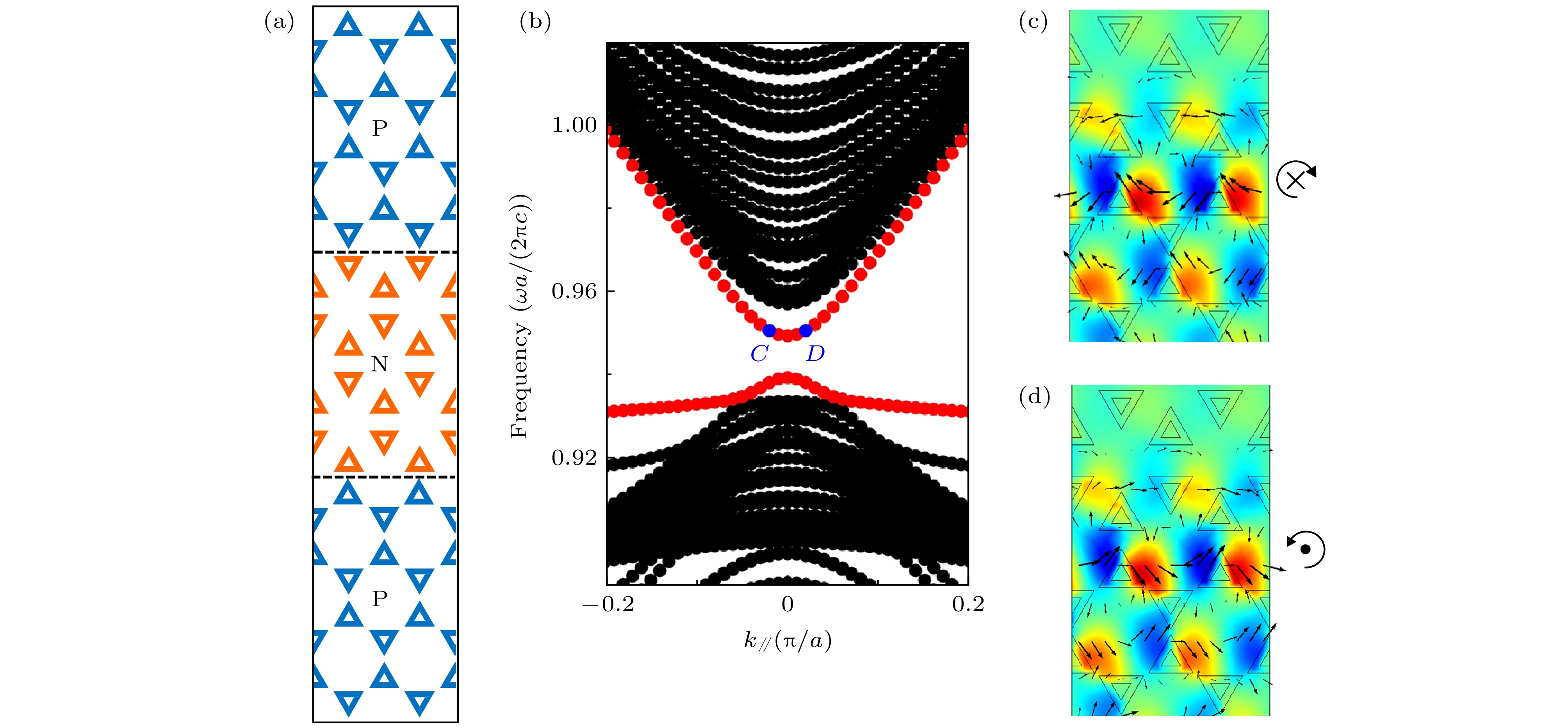
$\varGamma K$ 方向的投影带结构, 条带形的超原胞中间有20个非平庸原胞, 其两端各有10个平庸原胞, 红点和黑点分别表示边界态和体态; (c) C点所对应的磁场和平均能流密度在超原胞的下分界面上的分布; (d) 与图(c)相同, 但对应的是图(b)中的D点; 红色和蓝色分别代表磁场${H_z}$ 的正负最大值, 箭头显示能流的大小和方向Fig. 3. Project band structure and topological edge states: (a) Schematic of a ribbon-shaped supercell composed of topologically nontrivial crystal with its two edges cladded by topologically trivial crystals; (b) dispersion relation along ΓK direction for the ribbon-shaped supercell, the ribbon has 20 nontrivial unit cells in the middle and 10 trivial unit cells on both sides, the red and black dots display the edge and bulk states, respectively; (c) distribution of the magnetic field and time-averaged Poynting vector around the lower interface of the supercell, corresponding to point C indicated in panel (b); (d) the same as panel (c), but corresponding to the point D indicated in panel (b); the positive and negative maxima of the magnetic field,
${H_z}$ , are represented by dark red and dark blue, respectively, and the arrows show the direction and magnitude of the Poynting vector.图 5 赝自旋依赖的边界态沿zigzag型分界面的单向传输 (a) 由8个天线所组成的手性类点源示意图, 相邻天线的相位差为
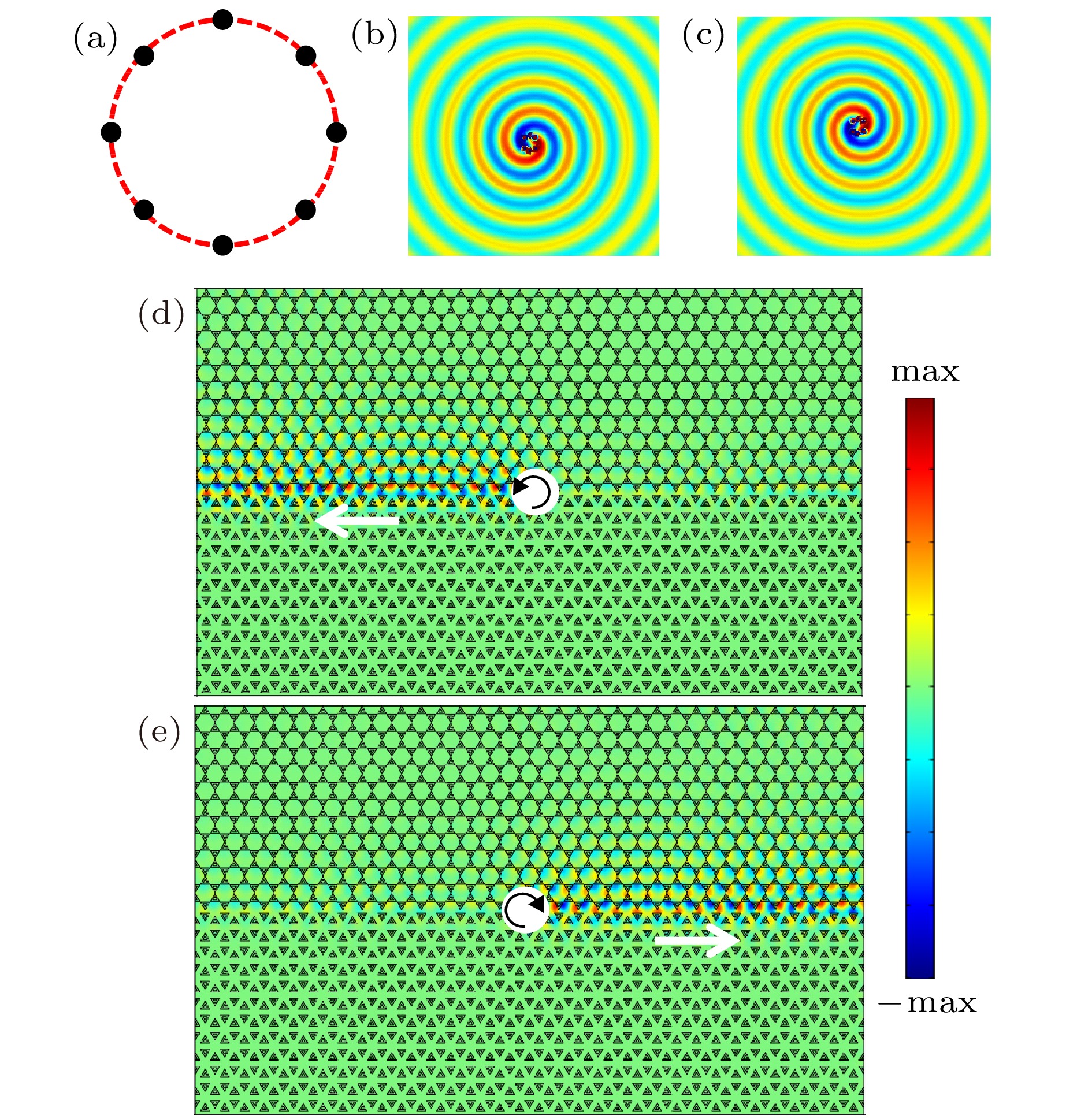
${{\text{π}} / 4}$ ; (b) 相位逆时针减小的手性类点源在空气中所激发的磁场分布; (c) 相位顺时针减小的手性类点源在空气中所激发的磁场分布; (d) 由(b)图中的源所激发的电磁波沿zigzag型分界面向左单向传输; (e) 由(c)图中的源所激发的电磁波沿zigzag型分界面向右单向传输. (d), (e)图所示结构的四周包围着完美匹配层; 手性类点源频率为$f \approx {{0.95 c} / a}$ , 白色圆标记源的位置, 其中的黑色箭头表示源的相位减小方向; 水平方向的白色箭头表示边界态的传输方向Fig. 5. Unidirectional propagation of the pseudospin-dependent edge states localized at the zigzag interface: (a) Schematic of a point-like chiral source made by an eight-antenna array with phase delay of
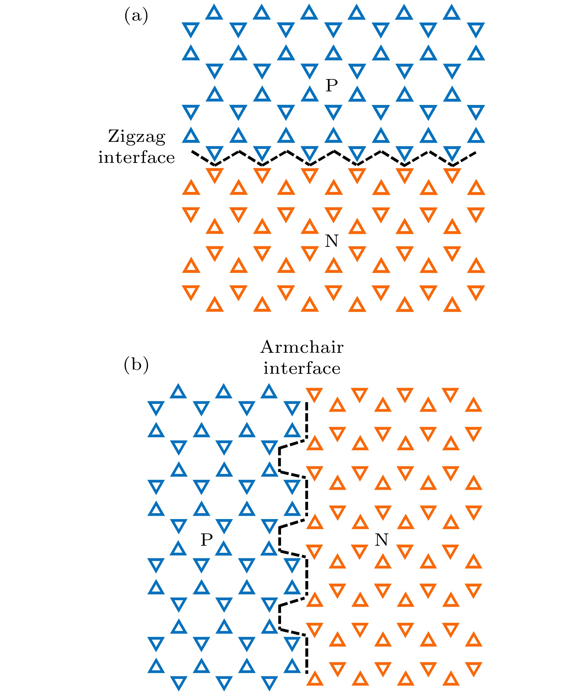
${{\text{π}} / 4}$ one by one; (b) magnetic field distribution stimulated by the point-like chiral source with an anticlockwise phase delay in the air; (c) magnetic field distribution stimulated by the point-like chiral source with a clockwise phase delay in the air; (d) leftward unidirectional electromagnetic wave propagation excited by the source in panel (b) along the zigzag interface; (e) rightward unidirectional electromagnetic wave propagation excited by the source in panel (c) along the zigzag interface. The structures in panel (d) and (e) are surrounded by the perfectly matched layers; the point-like chiral sources are marked as white circles with operating frequency$f \approx {{0.95 c} / a}$ , and their phase delay directions are repre-sented by black arrows; the white arrows along the horizontal direction indicate the propagation directions of the edge states.图 6 赝自旋依赖的边界态沿armchair型分界面的单向传输 (a) 相位逆时针减小的手性类点源所激发的电磁波沿armchair型分界面向下单向传输; (b) 相位顺时针减小的手性类点源所激发的电磁波沿armchair型分界面向上单向传输; 图中结构的四周包围着完美匹配层; 手性类点源频率为
$f \approx {{0.95 c} / a}$ , 白色圆标记源的位置, 其中的黑色箭头表示源的相位减小方向; 竖直方向的白色箭头表示边界态的传输方向Fig. 6. Unidirectional propagation of the pseudospin-dependent edge states localized at the armchair interface: (a) Downward unidirectional electromagnetic wave propagation excited by the point-like chiral source with an anticlockwise phase delay along the armchair interface; (b) upward unidirectional electromagnetic wave propagation excited by the point-like chiral source with a clockwise phase delay along the armchair interface. The structures are surrounded by the perfectly matched layers. The point-like chiral sources are marked as white circles with operating frequency
$f \approx {{0.95 c}/ a}$ , and their phase delay directions are represented by black arrows. The white arrows along the vertical direction indicate the propagation directions of the edge states.图 7 拓扑边界态的鲁棒性 (a) 频率
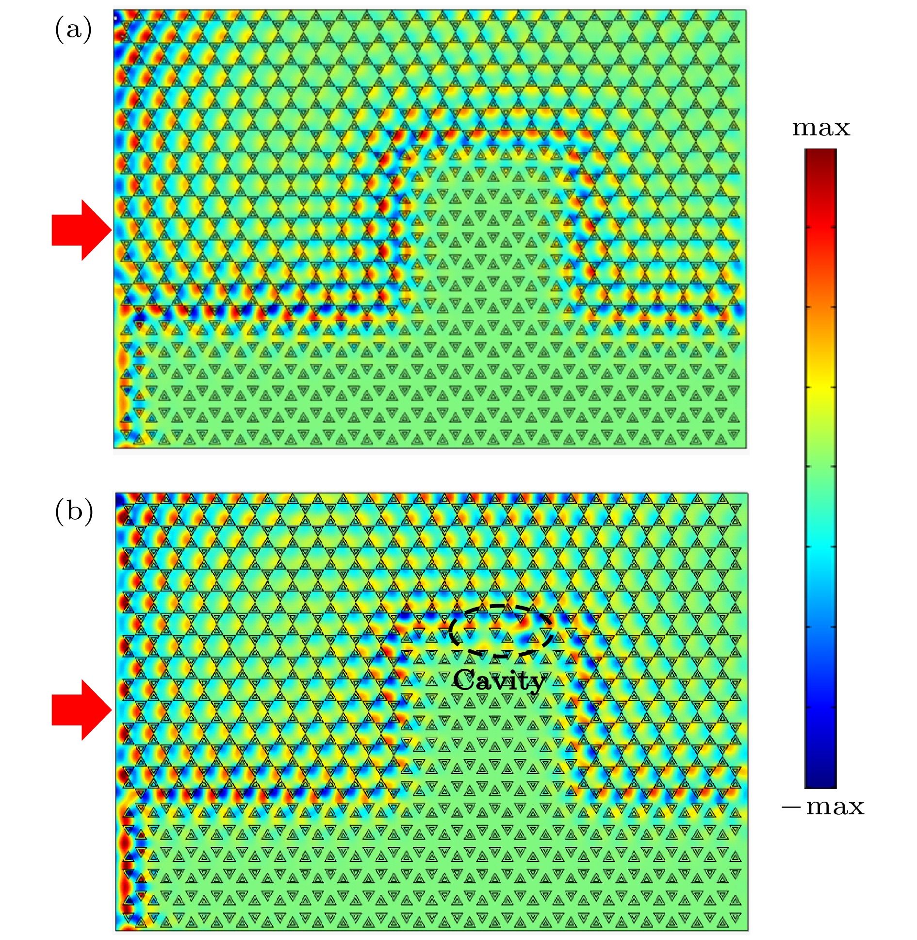
$f \approx {{0.95 c} / a}$ 的平面波入射到由P型和N型光子晶体组成的系统中所激发的磁场分布; (b) 与(a)图相同, 但在分界面上引入空穴缺陷(图中用椭圆形标出). 图中结构的四周包围着完美匹配层, 红色箭头表示入射方向, 拓扑边界态对分界面上的弯曲、空穴等缺陷免疫Fig. 7. Robustness of the topological edge states against defects: (a) Magnetic field distribution under the excitation of a plane wave with operating frequency
$f \approx {{0.95 c} / a}$ in the system consisting of P-type and N-type photonic crystals; (b) the same as panel (a), except that a cavity defect (displayed by ellipse) is introduced into the interface. The structures are surrounded by the perfectly matched layers. Red arrows represent the incident directions. The topological edge states are immune to various defects including sharp bend and cavity at the interface. -
[1] Klitzing K V, Dorda G, Pepper M 1980 Phys. Rev. Lett. 45 494
 Google Scholar
[2] König M, Wiedmann S, Brüne C, Roth A, Buhmann H, Molenkamp L W, Qi X L, Zhang S C 2007 Science 318 766
 Google Scholar
[3] Kane C L, Mele E J 2005 Phys. Rev. Lett. 95 226801
 Google Scholar
[4] Bernevig B A, Hughes T L, Zhang S C 2006 Science 314 1757
 Google Scholar
[5] Hasan M Z, Kane C L 2010 Rev. Mod. Phys. 82 3045
 Google Scholar
[6] Qi X L, Zhang S C 2011 Rev. Mod. Phys. 83 1057
 Google Scholar
[7] Haldane F D, Raghu S 2008 Phys. Rev. Lett. 100 013904
 Google Scholar
[8] Wang Z, Chong Y D, Joannopoulos J D, Soljačić M 2008 Phys. Rev. Lett. 100 013905
 Google Scholar
[9] Wang Z, Chong Y, Joannopoulos J D, Soljačić M 2009 Nature 461 772
 Google Scholar
[10] Skirlo S A, Lu L, Igarashi Y, Yan Q, Joannopoulos J, Soljačić M 2015 Phys. Rev. Lett. 115 253901
 Google Scholar
[11] Skirlo S A, Lu L, Soljačić M 2014 Phys. Rev. Lett. 113 113904
 Google Scholar
[12] Minkov M, Savona V 2016 Optica 3 200
 Google Scholar
[13] Liu K, Shen L, He S 2012 Opt. Lett. 37 4110
 Google Scholar
[14] Khanikaev A B, Mousavi S H, Tse W K, Kargarian M, MacDonald A H, Shvets G 2013 Nat. Mater. 12 233
 Google Scholar
[15] Chen W J, Jiang S J, Chen X D, Zhu B, Zhou L, Dong J W, Chan C T 2014 Nat. Commun. 5 5782
 Google Scholar
[16] He C, Sun X C, Liu X P, Lu M H, Chen Y, Feng L, Chen Y F 2016 Proc. Natl. Acad. Sci. USA 113 4924
 Google Scholar
[17] Hafezi M, Demler E A, Lukin M D, Taylor J M 2011 Nat. Phys. 7 907
 Google Scholar
[18] Fang K, Yu Z, Fan S 2012 Nat. Photonics 6 782
 Google Scholar
[19] Rechtsman M C, Zeuner J M, Plotnik Y, Lumer Y, Podolsky D, Dreisow F, Nolte S, Segev M, Szameit A 2013 Nature 496 196
 Google Scholar
[20] Lu L, Gao H, Wang Z 2018 Nat. Commun. 9 5384
 Google Scholar
[21] Lu L, Fang C, Fu L, Johnson S G, Joannopoulos J D, Soljačić M 2016 Nat. Phys. 12 337
 Google Scholar
[22] Yang Y, Gao Z, Xue H, Zhang L, He M, Yang Z, Singh R, Chong Y, Zhang B, Chen H 2019 Nature 565 622
 Google Scholar
[23] Wu L H, Hu X 2015 Phys. Rev. Lett. 114 223901
 Google Scholar
[24] Yang Y, Xu Y F, Xu T, Wang H X, Jiang J H, Hu X, Hang Z H 2018 Phys. Rev. Lett. 120 217401
 Google Scholar
[25] Zhu X, Wang H X, Xu C, Lai Y, Jiang J H, John S 2018 Phys. Rev. B 97 085148
 Google Scholar
[26] Chen Z G, Mei J, Sun X C, Zhang X, Zhao J, Wu Y 2017 Phys. Rev. A 95 043827
 Google Scholar
[27] Chen X D, Deng W M, Lu J C, Dong J W 2018 Phys. Rev. B 97 184201
 Google Scholar
[28] Kang Y, Ni X, Cheng X, Khanikaev A B, Genack A Z 2018 Nat. Commun. 9 3029
 Google Scholar
[29] Khanikaev A B, Fleury R, Mousavi S H, Alù A 2015 Nat. Commun. 6 8260
 Google Scholar
[30] Zhang Z, Tian Y, Cheng Y, Wei Q, Liu X, Christensen J 2018 Phys. Rev. Appl. 9 034032
 Google Scholar
[31] Wei Q, Tian Y, Zuo S Y, Cheng Y, Liu X J 2017 Phys. Rev. B 95 094305
 Google Scholar
[32] He H, Qiu C, Ye L, Cai X, Fan X, Ke M, Zhang F, Liu Z 2018 Nature 560 61
 Google Scholar
[33] Zhang Z, Tian Y, Cheng Y, Liu X, Christensen J 2017 Phys. Rev. B 96 241306
 Google Scholar
[34] Mei J, Chen Z, Wu Y 2016 Sci. Rep. 6 32752
 Google Scholar
[35] Neto A H C, Guinea F, Peres N M R, Novoselov K S, Geim A K 2009 Rev. Mod. Phys. 81 109
 Google Scholar
[36] Mei J, Wu Y, Chan C T, Zhang Z Q 2012 Phys. Rev. B 86 035141
 Google Scholar
[37] Li Y, Wu Y, Chen X, Mei J 2013 Opt. Express 21 7699
 Google Scholar
[38] Shen S Q, Shan W Y, Lu H Z 2011 Spin 1 33
 Google Scholar
计量
- 文章访问数: 20231
- PDF下载量: 638
- 被引次数: 0


 下载:
下载:


