-
AlGaN是制备深紫外光电器件和电子器件的重要材料. 随着Al组分的增加, AlGaN材料表面容易出现局域组分不均匀的相分离现象, 进而影响器件的性能. 为了探索相分离的微观机制, 本文采用了同位的共聚焦微区荧光光谱和扫描开尔文探针显微术对不同Al组分的AlGaN表面相分离现象进行了表征. 三片样品的Al组分比分别约为0.3, 0.5和0.7. 本文采用的基于双频锁相的单次扫描开尔文探针显微术, 可获得高空间分辨(约10 nm)的表面电势像. 在微区荧光光谱中出现明显相分离现象的区域, 利用此方法获得的表面电势像可以清晰地观察到犬牙交错的台阶及其表面凹坑边缘的电势变化, 对应组分的不均匀性. 随着台阶转入台阶流的形态, 表面凹坑逐渐缩小和合并, 台阶和凹坑边缘不再出现明显的电势畴界, 光谱中相分离的现象消失. 实验结果表明, AlGaN表面的台阶和凹坑边缘是产生组分不均匀性, 进而在光谱中产生相分离现象的主要原因; 结合同位微区荧光光谱, 高分辨的扫描开尔文探针显微术是一种有效的表征AlGaN相分离微观机制的方法.
-
关键词:
- 铝镓氮 /
- 相分离 /
- 扫描开尔文探针显微术 /
- 荧光光谱
AlGaN is a key material for deep ultraviolet optoelectronic and electronic devices. With the increase of the Al composition ratio, the phase separation on the surface, caused by small-scale compositional fluctuations, is prone to affecting the performance of the device. In order to explore the mechanism of the phase separation on a nanoscale, the AlGaN wafers with different quantities of Al compositions are investigated by the confocal photoluminescence spectroscopy and the single-pass Kelvin force probe microscopy. The composition ratios of Al for the three samples are about 0.3, 0.5, and 0.7, respectively. The single-pass Kelvin force probe microscopy based on dual-frequency phase-locking is used to obtain high spatially resolved (about 10 nm) surface potential images. In the area where the phase separation phenomenon is obvious in the photoluminescence spectrum, the sharp change of the surface potential can be observed at the irregular steps and the edges of the surface pits. The potential changes can be ascribed to the inhomogeneous composition distribution. In the area where the topography turns into step flow, the surface pits shrink and merge. No obvious surface potential domain boundaries appear at the steps nor on the edges of the surface pits. Meanwhile, the phase separation phenomenon in the photoluminescence spectrum almost disappears. Our experiments show that the steps and the edges of the surface pits on AlGaN surfaces are main reasons for small-scale compositional fluctuations and the phase separation in the spectrum. Combining with in-situ confocal photoluminescence spectra, high spatially resolved surface potential image by single-pass Kelvin force probe microscopy is an effective method to characterize the phase separation on AlGaN surface on a nanoscale.[1] Cai Q, Li Q, Li M, Tang Y, Wang J, Xue J J, Chen D J, Lu H, Zhang R, Zheng Y D 2019 IEEE Photonics J. 11 6801507
 Google Scholar
[2] Li D B, Jiang K, Sun X J, Guo C L 2018 Adv. Opt. Photonics 10 43
 Google Scholar
[3] Yang W H, Li J C, Lin W, Li S P, Chen H Y, Liu D Y, Yang X, Kang J Y 2013 AIP Adv. 3 052103
 Google Scholar
[4] 刘静, 王琳倩, 黄忠孝 2019 物理学报 68 248501
 Google Scholar
Liu J, Wang L Q, Huang Z X 2019 Acta Phys. Sin. 68 248501
 Google Scholar
[5] 张志荣, 房玉龙, 尹甲运, 郭艳敏, 王波, 王元刚, 李佳, 芦伟立, 高楠, 刘沛, 冯志红 2018 物理学报 67 076801
 Google Scholar
Zhang Z R, Fang Y L, Yin J Y, Guo Y M, Wang B, Wang Y G, Li J, Lu W L, Gao N, Liu P, Feng Z H 2018 Acta Phys. Sin. 67 076801
 Google Scholar
[6] 唐文昕, 郝荣晖, 陈扶, 于国浩, 张宝顺 2018 物理学报 67 198501
 Google Scholar
Tang W X, Hao R H, Chen F, Yu G H, Zhang B S 2018 Acta Phys. Sin. 67 198501
 Google Scholar
[7] 张力, 林志宇, 罗俊, 王树龙, 张进成, 郝跃, 戴扬, 陈大正, 郭立新 2017 物理学报 66 247302
 Google Scholar
Zhang L, Lin Z Y, Lou J, Wang S L, Zhang J C, Hao Y, Dai Y, Chen D Z, Guo L X 2017 Acta Phys. Sin. 66 247302
 Google Scholar
[8] 郭海君, 段宝兴, 袁嵩, 谢慎隆, 杨银堂 2017 物理学报 66 167301
 Google Scholar
Guo H J, Duan B X, Yuan S, Xie S L, Yang Y T 2017 Acta Phys. Sin. 66 167301
 Google Scholar
[9] Chen P, Chua S J, Miao Z L 2004 J. Cryst. Growth 273 74
 Google Scholar
[10] Pinos A, Liuolia V, Marcinkevicius S, Yang J, Gaska R, Shur M S 2011 J. Appl. Phys. 109 113516
 Google Scholar
[11] Wang X L, Zhao D G, Jiang D S, Yang H, Liang J W, Jahn U, Ploog K 2007 J. Phys. Condens. Matter 19 176005
 Google Scholar
[12] Bryan I, Bryan Z, Mita S, Rice A, Hussey L, Shelton C, Tweedie J, Maria J P, Collazo R, Sitar Z 2016 J. Cryst. Growth 451 65
 Google Scholar
[13] Jiang K, Sun X J, Ben J W, Shi Z M, Jia Y P, Wu Y, Kai C H, Wang Y, Li D B 2019 Crystengcomm 21 4864
 Google Scholar
[14] Luong T T, Ho Y-T, Wong Y Y, Chang S, Chang E Y 2018 Microelectron. Reliab. 83 286
 Google Scholar
[15] Knauer A, Kueller V, Zeimer U, Weyers M, Reich C, Kneissl M 2013 Phys. Status Solidi A 210 451
 Google Scholar
[16] Sun Q, Wang H, Jiang D S, Jin R Q, Huang Y, Zhang S M, Yang H, Jahn U, Ploog K H 2006 J. Appl. Phys. 100 123101
 Google Scholar
[17] Marcinkevicius S, Jain R, Shatalov M, Yang J, Shur M, Gaska R 2014 Appl. Phys. Lett. 105 241108
 Google Scholar
[18] Pinos A, Marcinkevicius S, Liuolia V, Yang J W, Gaska R, Shur M S 2012 Physica Status Solidi C: Current Topics in Solid State Physics Royal Inst Technol (KTH), Stockholm, Sweden, Jun 19–23, 2011 p1617
[19] Tamulaitis G 2011 Mater. Sci.-Medzg. 17 343
 Google Scholar
[20] Li G Y, Mao B, Lan F, Liu L M 2012 Rev. Sci. Instrum. 83 113701
 Google Scholar
[21] Liu Y, Li Q X, Wan L Y, Kucukgok B, Ghafari E, Ferguson I T, Zhang X, Wang S C, Feng Z C, Lu N 2017 Appl. Surf. Sci. 421 389
 Google Scholar
[22] Tauc J, Grigorovici R, Vancu A 1966 Phys. Status Solidi 15 627
 Google Scholar
[23] Koide Y, Itoh H, Khan M R H, Hiramatu K, Sawaki N, Akasaki I 1987 J. Appl. Phys. 61 4540
 Google Scholar
[24] Takeuchi K, Adachi S, Ohtsuka K 2010 J. Appl. Phys. 107 023306
 Google Scholar
[25] Nepal N, Li J, Nakarmi M L, Lin J Y, Jiang H X 2005 Appl. Phys. Lett. 87 242104
 Google Scholar
[26] Nepal N, Nakarmi M L, Lin J Y, Jiang H X 2006 Appl. Phys. Lett. 89 092107
 Google Scholar
[27] Sun Q, Huang Y, Wang H, Chen J, Jin R Q, Zhang S M, Yang H, Jiang D S, Jahn U, Ploog K H 2005 Appl. Phys. Lett. 87 121914
 Google Scholar
-
图 1 (a) Al0.3Ga0.7N样品剖面的SEM图; (b) Al0.5Ga0.5N样品剖面的SEM图; (c) Al0.7Ga0.3N样品剖面的SEM图; (a), (b)和(c)图中分别用红框和黄框标记了AlGaN层与AlN层的位置, 并在框中显示了测量得到的厚度; (d)中从左至右分别为Al0.3Ga0.7N, Al0.5Ga0.5N和Al0.7Ga0.3N样品利用椭偏仪测量得到的吸收系数拟合带隙的结果
Fig. 1. (a) The SEM image of the Al0.3Ga0.7N Sample; (b) the SEM image of the Al0.5Ga0.5N Sample; (c) the SEM image of the Al0.7Ga0.3N Sample. The AlGaN and AlN layers in (a), (b) and (c) are marked with red and yellow squares respectively, in addition with the thickness labeled. (d) From left to right, the curves show the absorption coefficients of Al0.3Ga0.7N, Al0.5Ga0.5N and Al0.7Ga0.3N samples, respectively. The absorption coefficients are measured by an ellipsometer and the band gaps are fitted out and labeled.
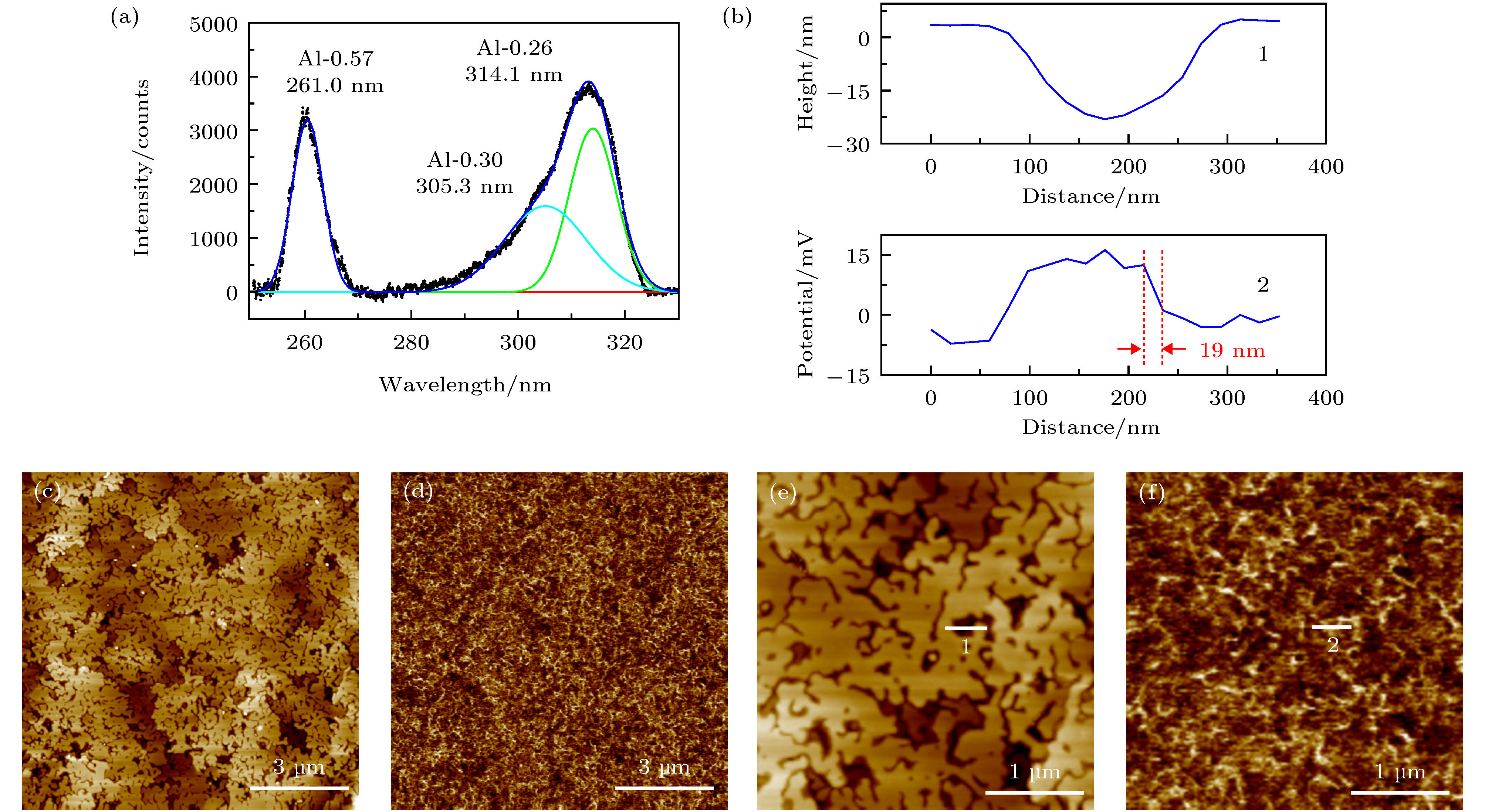
图 2 Al0.5Ga0.5N样品表面有明显相分离现象的区域 (a)该区域的典型荧光光谱; (b)上图和下图分别为形貌和表面电势的剖面图, 对应于图(e)中标记1的位置和图(f)中标记2的位置; 如红线所示, 下图中电势剖面图的下降沿宽度约为19 nm, 说明了我们采用的双频单次扫描开尔文探针显微术的典型空间分辨率; (c)和(d)扫描尺寸为10 μm时的表面形貌像及对应表面电势像; (e) 和 (f)扫描尺寸为3 μm时的表面形貌像及对应表面电势像; 图(e)中白色横线标记1和图(f)中标记2对应同一位置
Fig. 2. The area with obvious phase separation phenomenon on the Al0.5Ga0.5N sample surface. (a) A typical photoluminescence spectrum of the area. (b) Profiles of the topography and the surface potential shown in plot 1 and 2, respectively. The profile of the topography is extracted from mark 1 in panel (e). The profile of the surface potential is extracted from the mark 2 in panel (f). The width of the falling edge marked by red lines in the profile of the surface potential is about 19 nm. This value presents the typical spatial resolution of the single-pass Kelvin force probe microscopy we applied. (c) and (d) The topography image and the surface potential image, respectively, obtained at the same area with a scan size of 10 μm. (e) and (f) The topography image and the surface potential image, respectively, obtained at the same area with a scan size of 3 μm. The white lines marked by 1 in panel (e) and 2 in panel (f) are picked at the same position.
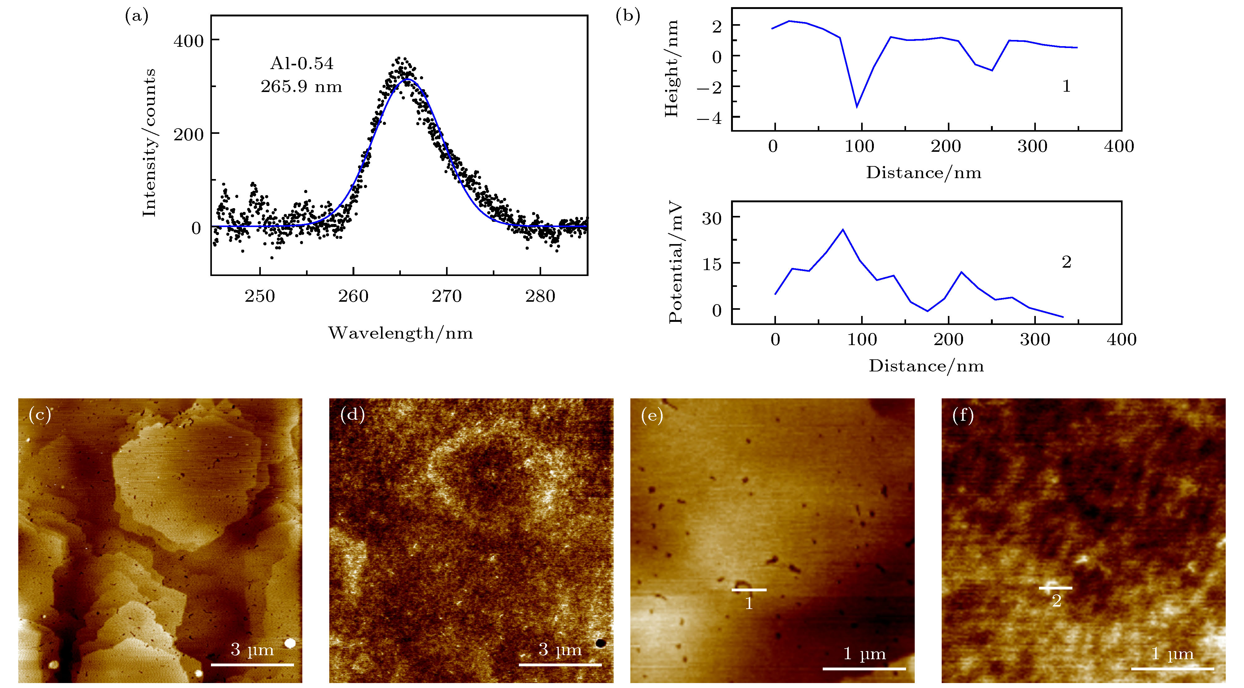
图 3 Al0.5Ga0.5N样品表面没有明显相分离现象的区域 (a) 该区域的典型荧光光谱; (b)上图和下图分别为形貌和表面电势的剖面图, 对应图(e)中标记1的位置和图(f)中标记2的位置; (c) 和 (d) 扫描尺寸为10 μm时的表面形貌像及对应表面电势像; (e)和(f) 扫描尺寸为3 μm时的表面形貌像及对应表面电势像; 图(e)中白色横线标记1和图(f)中标记2对应同一位置
Fig. 3. The area without phase separation phenomenon on the Al0.5Ga0.5N sample surface. (a) A typical photoluminescence spectrum of the area. (b) Profiles of the topography and the surface potential shown in the plot 1 and 2, respectively. The profile of the topography is extracted from mark 1 in panel (e). The profile of the surface potential is extracted from the mark 2 in panel (f). (c) and (d) The topography image and the surface potential image, respectively, obtained at the same area with a scan size of 10 μm. (e) and (f) The topography image and the surface potential image, respectively, obtained at the same area with a scan size of 3 μm. The white lines marked by 1 in panel (e) and 2 in panel (f) are picked at the same position.
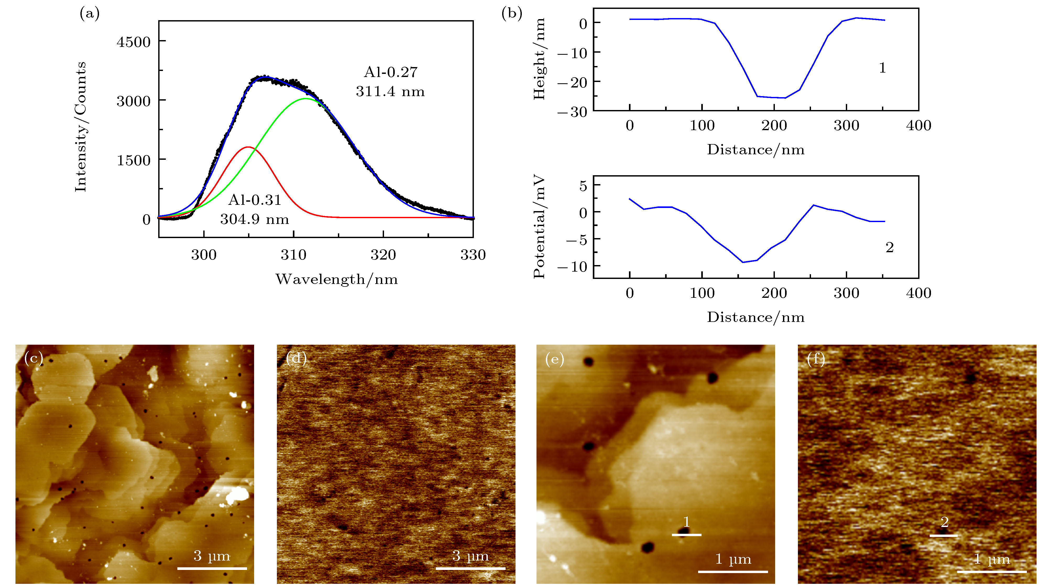
图 4 Al0.3Ga0.7N样品表面 (a) 该区域的典型荧光光谱; (b)上图和下图分别为形貌和表面电势的剖面图, 对应图(e)中标记1的位置和图(f)中标记2的位置; (c)和(d)扫描尺寸为10 μm时的表面形貌像及对应表面电势像; (e)和(f)扫描尺寸为3 μm时的表面形貌像及对应表面电势像; 图(e) 中白色横线标记1和图(f)中标记2对应同一位置
Fig. 4. The area on the Al0.3Ga0.7N sample surface. (a) A typical photoluminescence spectrum of the area. (b) Profiles of the topography and the surface potential shown in the plot 1 and 2, respectively. The profile of the topography is extracted from mark 1 in panel (e). The profile of the surface potential is extracted from the mark 2 in panel (f). (c) and (d) The topography image and the surface potential image, respectively, obtained at the same area with a scan size of 10 μm. (e) and (f) The topography image and the surface potential image, respectively, obtained at the same area with a scan size of 3 μm. The white lines marked by 1 in panel (e) and 2 in panel (f) are picked at the same position.
图 5 Al0.7Ga0.3N样品表面 (a) 该区域的典型荧光光谱; (b)上图和下图分别为形貌和表面电势的剖面图, 对应图(e)中标记1的位置和图(f)中标记2的位置; (c)和(d)扫描尺寸为10 μm的表面形貌像及对应表面电势像; (e) 和 (f)扫描尺寸为3 μm时的表面形貌像及对应表面电势像; 图(e) 中白色横线标记1和图(f)中标记2对应同一位置
Fig. 5. The area on the Al0.7Ga0.3N sample surface. (a) A typical photoluminescence spectrum of the area. (b) profiles of the topography and the surface potential shown in the plot 1 and 2, respectively. The profile of the topography is extracted from mark 1 in panel (e). the profile of the surface potential is extracted from the mark 2 in panel (f). (c) and (d) the topography image and the surface potential image, respectively, obtained at the same area with a scan size of 10 μm. (e) and (f) the topography image and the surface potential image, respectively, obtained at the same area with a scan size of 3 μm. The white lines marked by 1 in panel (e) and 2 in panel (f) are picked at the same position.
-
[1] Cai Q, Li Q, Li M, Tang Y, Wang J, Xue J J, Chen D J, Lu H, Zhang R, Zheng Y D 2019 IEEE Photonics J. 11 6801507
 Google Scholar
[2] Li D B, Jiang K, Sun X J, Guo C L 2018 Adv. Opt. Photonics 10 43
 Google Scholar
[3] Yang W H, Li J C, Lin W, Li S P, Chen H Y, Liu D Y, Yang X, Kang J Y 2013 AIP Adv. 3 052103
 Google Scholar
[4] 刘静, 王琳倩, 黄忠孝 2019 物理学报 68 248501
 Google Scholar
Liu J, Wang L Q, Huang Z X 2019 Acta Phys. Sin. 68 248501
 Google Scholar
[5] 张志荣, 房玉龙, 尹甲运, 郭艳敏, 王波, 王元刚, 李佳, 芦伟立, 高楠, 刘沛, 冯志红 2018 物理学报 67 076801
 Google Scholar
Zhang Z R, Fang Y L, Yin J Y, Guo Y M, Wang B, Wang Y G, Li J, Lu W L, Gao N, Liu P, Feng Z H 2018 Acta Phys. Sin. 67 076801
 Google Scholar
[6] 唐文昕, 郝荣晖, 陈扶, 于国浩, 张宝顺 2018 物理学报 67 198501
 Google Scholar
Tang W X, Hao R H, Chen F, Yu G H, Zhang B S 2018 Acta Phys. Sin. 67 198501
 Google Scholar
[7] 张力, 林志宇, 罗俊, 王树龙, 张进成, 郝跃, 戴扬, 陈大正, 郭立新 2017 物理学报 66 247302
 Google Scholar
Zhang L, Lin Z Y, Lou J, Wang S L, Zhang J C, Hao Y, Dai Y, Chen D Z, Guo L X 2017 Acta Phys. Sin. 66 247302
 Google Scholar
[8] 郭海君, 段宝兴, 袁嵩, 谢慎隆, 杨银堂 2017 物理学报 66 167301
 Google Scholar
Guo H J, Duan B X, Yuan S, Xie S L, Yang Y T 2017 Acta Phys. Sin. 66 167301
 Google Scholar
[9] Chen P, Chua S J, Miao Z L 2004 J. Cryst. Growth 273 74
 Google Scholar
[10] Pinos A, Liuolia V, Marcinkevicius S, Yang J, Gaska R, Shur M S 2011 J. Appl. Phys. 109 113516
 Google Scholar
[11] Wang X L, Zhao D G, Jiang D S, Yang H, Liang J W, Jahn U, Ploog K 2007 J. Phys. Condens. Matter 19 176005
 Google Scholar
[12] Bryan I, Bryan Z, Mita S, Rice A, Hussey L, Shelton C, Tweedie J, Maria J P, Collazo R, Sitar Z 2016 J. Cryst. Growth 451 65
 Google Scholar
[13] Jiang K, Sun X J, Ben J W, Shi Z M, Jia Y P, Wu Y, Kai C H, Wang Y, Li D B 2019 Crystengcomm 21 4864
 Google Scholar
[14] Luong T T, Ho Y-T, Wong Y Y, Chang S, Chang E Y 2018 Microelectron. Reliab. 83 286
 Google Scholar
[15] Knauer A, Kueller V, Zeimer U, Weyers M, Reich C, Kneissl M 2013 Phys. Status Solidi A 210 451
 Google Scholar
[16] Sun Q, Wang H, Jiang D S, Jin R Q, Huang Y, Zhang S M, Yang H, Jahn U, Ploog K H 2006 J. Appl. Phys. 100 123101
 Google Scholar
[17] Marcinkevicius S, Jain R, Shatalov M, Yang J, Shur M, Gaska R 2014 Appl. Phys. Lett. 105 241108
 Google Scholar
[18] Pinos A, Marcinkevicius S, Liuolia V, Yang J W, Gaska R, Shur M S 2012 Physica Status Solidi C: Current Topics in Solid State Physics Royal Inst Technol (KTH), Stockholm, Sweden, Jun 19–23, 2011 p1617
[19] Tamulaitis G 2011 Mater. Sci.-Medzg. 17 343
 Google Scholar
[20] Li G Y, Mao B, Lan F, Liu L M 2012 Rev. Sci. Instrum. 83 113701
 Google Scholar
[21] Liu Y, Li Q X, Wan L Y, Kucukgok B, Ghafari E, Ferguson I T, Zhang X, Wang S C, Feng Z C, Lu N 2017 Appl. Surf. Sci. 421 389
 Google Scholar
[22] Tauc J, Grigorovici R, Vancu A 1966 Phys. Status Solidi 15 627
 Google Scholar
[23] Koide Y, Itoh H, Khan M R H, Hiramatu K, Sawaki N, Akasaki I 1987 J. Appl. Phys. 61 4540
 Google Scholar
[24] Takeuchi K, Adachi S, Ohtsuka K 2010 J. Appl. Phys. 107 023306
 Google Scholar
[25] Nepal N, Li J, Nakarmi M L, Lin J Y, Jiang H X 2005 Appl. Phys. Lett. 87 242104
 Google Scholar
[26] Nepal N, Nakarmi M L, Lin J Y, Jiang H X 2006 Appl. Phys. Lett. 89 092107
 Google Scholar
[27] Sun Q, Huang Y, Wang H, Chen J, Jin R Q, Zhang S M, Yang H, Jiang D S, Jahn U, Ploog K H 2005 Appl. Phys. Lett. 87 121914
 Google Scholar
计量
- 文章访问数: 11496
- PDF下载量: 155
- 被引次数: 0


 下载:
下载:


