


-
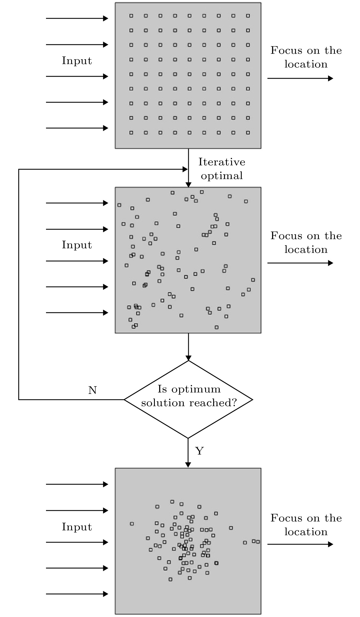
在光学材料与器件中, 由于不同波长的光会以不同速度传播, 因此一束复色光经过单个光学器件后会产生色散, 导致普通透镜不同波长的光无法合焦. 传统的聚焦系统可通过叠加多个透镜解决这一问题, 但这是以增加系统的复杂度、质量和成本为代价, 不适用于高集成度的纳米光学系统. 目前比较好的解决方法是平面超透镜, 即利用超表面对各点的振幅、相位、偏振等进行空间调控, 达到合焦的目的, 但这种平面超透镜难以直接片上集成. 本文将有限元法与遗传算法相组合发展出一种智能算法, 优化出一种宽带高效聚焦的片上集成纳米透镜. 该透镜尺寸只有2 μm × 2 μm, 可实现波长从470 nm至1734 nm的低色散聚焦, 能将大小为2 μm的激光光束通过透镜与波导的耦合聚焦成200 nm以下的光束, 耦合传播效率可达80%以上. 同时, 该智能算法能够适用于不同的纳米结构, 均可获得类似的聚焦效果和高效的耦合传播效率. 该工作为宽带高效的纳米透镜提供了重要思路, 也为实现高密度集成的纳米光子器件提供了新途径.As a basic optical element, optical lens is widely used for realizing the focusing, imaging and optical communication systems. Light of different wavelengths will propagate at different speeds. A beam of polychromatic light will produce chromatic dispersion after passing through a single optical device, which prevents the ordinary lenses from focusing the light of different wavelengths into a point. This means that the light of different wavelengths cannot be focused ideally. Traditional focusing systems can solve this problem by superimposing multiple lenses, but this is at the expense of increasing the complexity, weight, and cost of the system, and is not suitable for highly integrated nano-optical systems. At present, a better solution is to use the plane metalens, that is, using the metasurface to control the amplitude, phase and polarization at each point in space. However, the plane metalens is difficult to directly integrate on the chip. An intelligent algorithm developed by combining finite element method with genetic algorithm is used to optimize the design of multi-channel on-chip wavelength router devices and polarization router devices. In this paper, combining with years’ research results of the theory of multiple scattering coherent superposition of disordered media, the use of intelligent algorithm to design an on-chip integrated nano-lens that can achieve efficient focusing from the visible to the near infrared band. In the lens structure SiO2 serves as a substrate, and the arrangement structure of SiC rectangular column is designed. The substrate size is only 2 μm × 2 μm. The lens achieves low-dispersion focusing in the band from 470 nm to 1734 nm, with a focusing efficiency of over 55% at the highest level and 30% at the lowest level, and an average focusing efficiency of 42.1%. A 200-nm waveguide is added behind the focusing region. After refocusing through the waveguide, the laser beam with a size of 2 μm can be focused by the coupling of the lens and the waveguide into a beam below 200 nm in size. The focusing efficiency goes up to 80%. At the same time, the intelligent algorithm can be applied to different types of structures. The focusing lens structures composed of triangle, diamond, or circular nano columns are designed, which can achieve an approximate focusing effect and efficient coupling propagation efficiency. This work provides important ideas for developing broadband and efficient focusing nano-lens, as well as a new way to achieve the high-density integrated nanophotonic devices.
[1] Molesky S, Lin Z, Piggott A Y, Jin W, Vucković J, Rodriguez A W 2018 Nat. Photonics 12 659
 Google Scholar
[2] Tanemura T, Balram K C, Ly-Gagnon D S, Wahl P, White J S, Brongersma M L, Miller D A B 2011 Nano Lett. 11 2693
Google Scholar
[3] Yu N, Genevet P, Kats M A, Aieta F, Tetienne J, Capasso F, Gaburro Z 2011 Science 334 333
Google Scholar
[4] Khorasaninejad M, Chen W T, Devlin R C, Oh J, Zhu A Y, Capasso F 2016 Science 352 1190
Google Scholar
[5] Shrestha S, Overvig A C, Lu M, Stein A, Yu N 2018 Light Sci. Appl. 7 1081
Google Scholar
[6] Liu Z H, Liu X H, Xiao Z Y, Lu C C, Wang H Q, Wu Y, Hu X Y, Liu Y C, Zhang H Y, Zhang X D 2019 Optica 6 1367
Google Scholar
[7] Lu C C, Liu Z H, Wu Y, Xiao Z Y, Yu D Y, Zhang H Y, Wang C Y, Hu X Y, Liu Y C, Liu X Y, Zhang X D 2020 Adv. Opt. Mater. 8 1902018
Google Scholar
[8] 王慧琴, 龚旗煌 2013 物理学报 62 214202
Google Scholar
Wang H Q, Gong Q H 2013 Acta Phys. Sin. 62 214202
Google Scholar
[9] 王慧琴, 方利广, 王一凡, 余奥列 2011 物理学报 60 014203
Google Scholar
Wang H Q, Fang L G, Wang Y F, Yu A L 2011 Acta Phys. Sin. 60 014203
Google Scholar
[10] 刘正东, 王慧琴 2009 物理学报 58 1648
Google Scholar
Liu Z D, Wang H Q 2009 Acta Phys. Sin. 58 1648
Google Scholar
[11] Wang H Q, Ou Y H, Han D F, Wang Y F 2011 Optoelectronics Lett. 7 179
Google Scholar
[12] 王慧琴, 刘正东 2006 物理学报 55 2281
Google Scholar
Wang H Q, Liu Z D 2006 Acta Phys. Sin. 55 2281
Google Scholar
[13] Anderson P W 1958 Phys. Rev. 109 1492
Google Scholar
[14] John S 1991 Phys. Today 44 32
Google Scholar
[15] Cao H, Xu J Y, Seelig E W, Chang R P H 2000 Appl. Phys. Lett. 76 2997
Google Scholar
[16] Lu J, Vucković J 2013 Opt. Express 21 13351
Google Scholar
[17] Forrest S 1993 Science 261 872
Google Scholar
[18] Goh J, Fushman I, Englund D, Vucković J 2007 Opt. Express 15 8218
Google Scholar
[19] 张静娟, 姬扬, 姚德成, 陈俊本 1996 物理学报 45 789
Google Scholar
Zhang J J, Ji Y, Yao D C, Chen J B 1996 Acta Phys. Sin. 45 789
Google Scholar
-
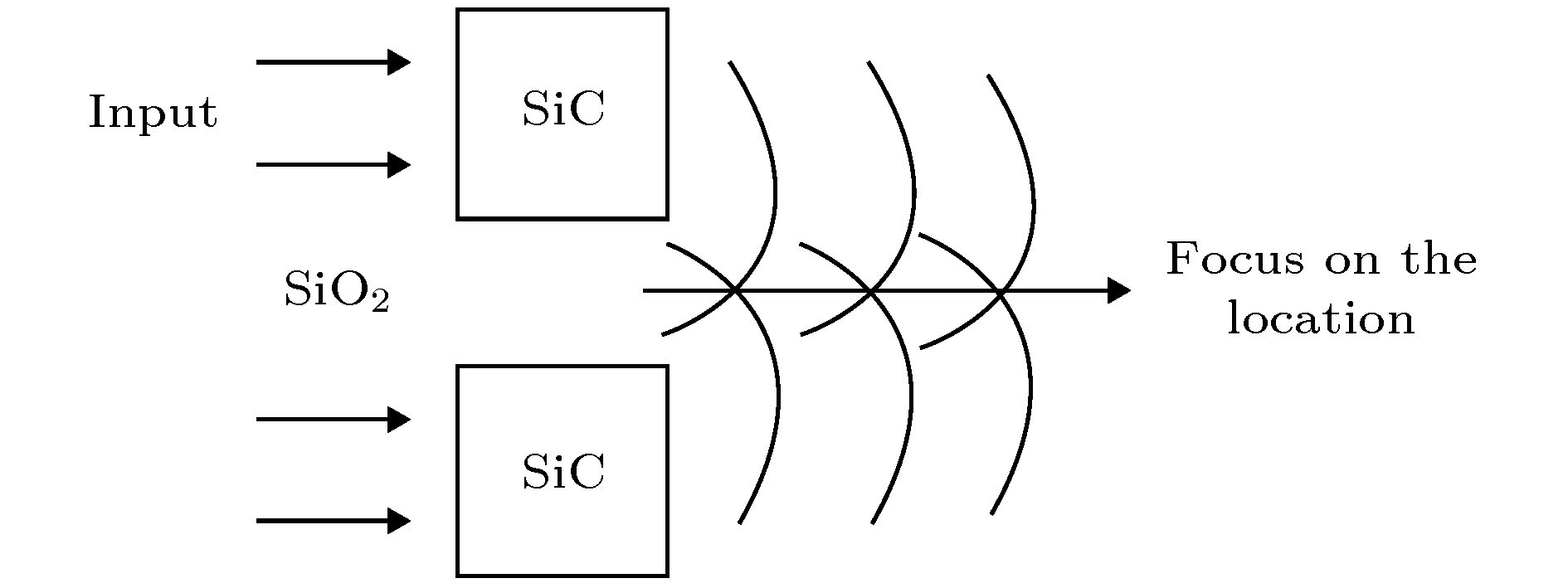
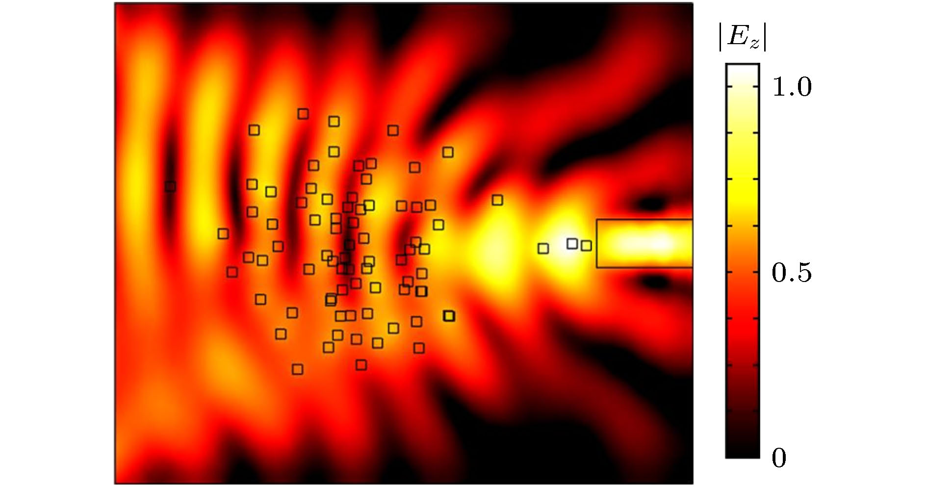
图 1 光经过碳化硅矩形后的衍射与干涉
Fig. 1. Diffraction and interference of light after passing through the silicon carbide rectangle.
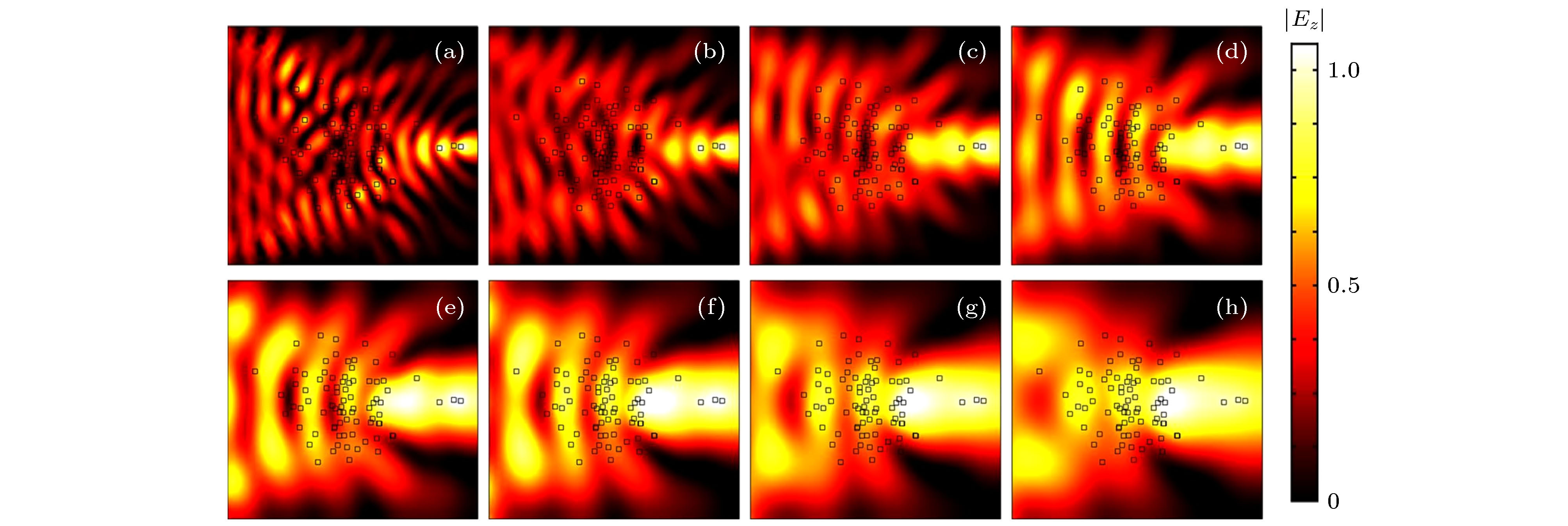
图 3 不同波长下电场幅值分布图 (a) 500 nm; (b) 650 nm; (c) 800 nm; (d) 950 nm; (e) 1100 nm; (f) 1250 nm; (g) 1400 nm; (h) 1550 nm
Fig. 3. Distribution of the electric field intensity of different wavelength: (a) 500 nm; (b) 650 nm; (c) 800 nm; (d) 950 nm; (e) 1100 nm; (f) 1250 nm; (g) 1400 nm; (h) 1550 nm.
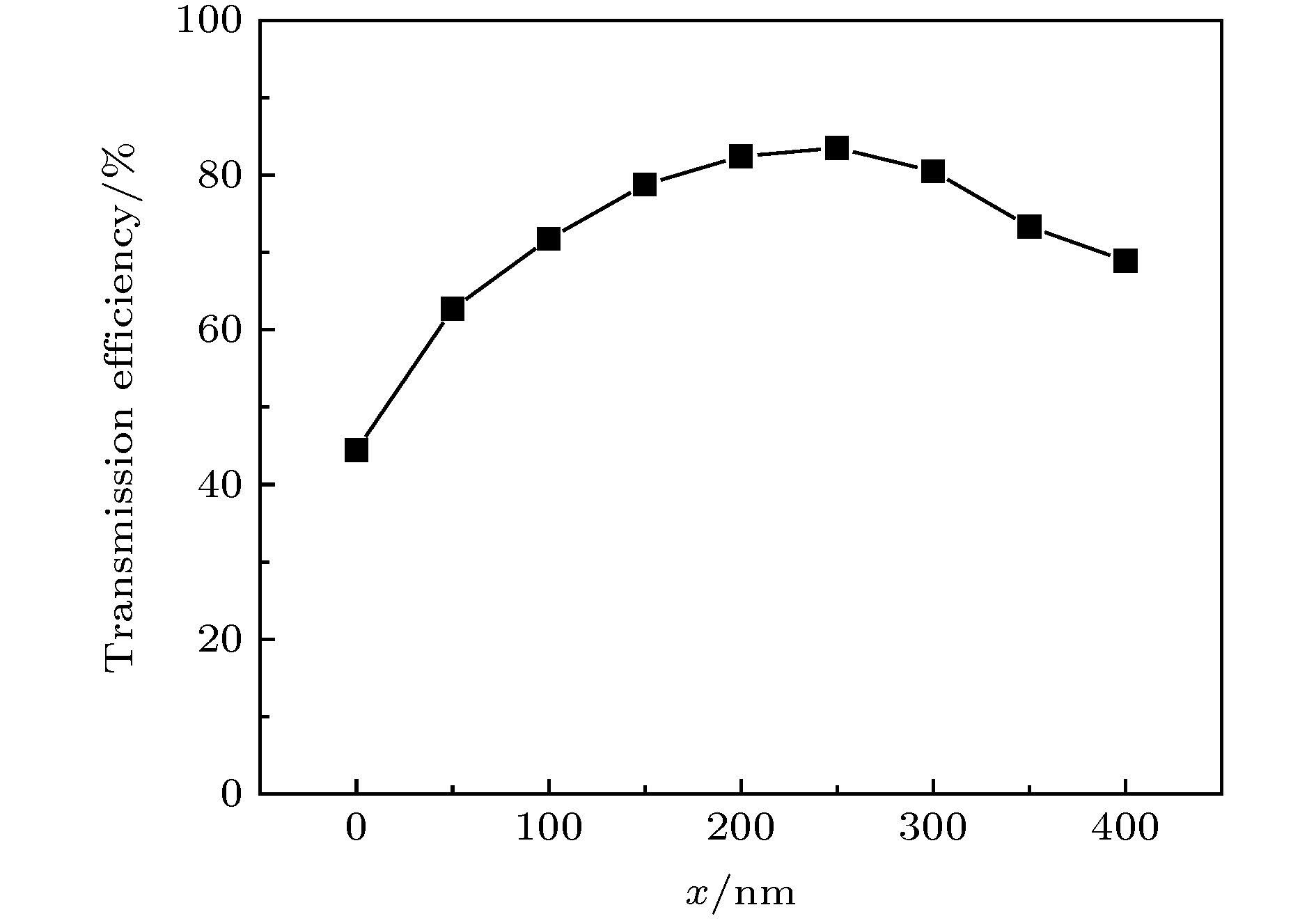
图 6 光经透镜后在波导中的传播效率
Fig. 6. Propagation efficiency of light in a waveguide after passing through the lens.

图 7 纳米柱结构与800 nm场幅值分布 (a) 三角形结构; (b) 菱形结构; (c) 圆形结构; (d) 三角形结构场幅值分布; (e) 菱形结构场幅值分布; (f) 圆形结构场幅值分布
Fig. 7. Nanoparticle structure and distribution of the electric field intensity at 800 nm: (a) Triangular structure; (b) rhombic structure; (c) circular structure; (d) the electric field intensity distribution of triangular structure; (e) the electric field intensity distribution of rhombic structure; (f) the electric field intensity distribution of circular structure.

图 8 聚焦效率 (a) 三角形结构; (b) 菱形结构; (c) 圆形结构
Fig. 8. Focusing efficiency: (a) Triangular structure; (b) rhombic structure; (c) circular structure.
-
[1] Molesky S, Lin Z, Piggott A Y, Jin W, Vucković J, Rodriguez A W 2018 Nat. Photonics 12 659
Google Scholar
[2] Tanemura T, Balram K C, Ly-Gagnon D S, Wahl P, White J S, Brongersma M L, Miller D A B 2011 Nano Lett. 11 2693
Google Scholar
[3] Yu N, Genevet P, Kats M A, Aieta F, Tetienne J, Capasso F, Gaburro Z 2011 Science 334 333
Google Scholar
[4] Khorasaninejad M, Chen W T, Devlin R C, Oh J, Zhu A Y, Capasso F 2016 Science 352 1190
Google Scholar
[5] Shrestha S, Overvig A C, Lu M, Stein A, Yu N 2018 Light Sci. Appl. 7 1081
Google Scholar
[6] Liu Z H, Liu X H, Xiao Z Y, Lu C C, Wang H Q, Wu Y, Hu X Y, Liu Y C, Zhang H Y, Zhang X D 2019 Optica 6 1367
Google Scholar
[7] Lu C C, Liu Z H, Wu Y, Xiao Z Y, Yu D Y, Zhang H Y, Wang C Y, Hu X Y, Liu Y C, Liu X Y, Zhang X D 2020 Adv. Opt. Mater. 8 1902018
Google Scholar
[8] 王慧琴, 龚旗煌 2013 物理学报 62 214202
Google Scholar
Wang H Q, Gong Q H 2013 Acta Phys. Sin. 62 214202
Google Scholar
[9] 王慧琴, 方利广, 王一凡, 余奥列 2011 物理学报 60 014203
Google Scholar
Wang H Q, Fang L G, Wang Y F, Yu A L 2011 Acta Phys. Sin. 60 014203
Google Scholar
[10] 刘正东, 王慧琴 2009 物理学报 58 1648
Google Scholar
Liu Z D, Wang H Q 2009 Acta Phys. Sin. 58 1648
Google Scholar
[11] Wang H Q, Ou Y H, Han D F, Wang Y F 2011 Optoelectronics Lett. 7 179
Google Scholar
[12] 王慧琴, 刘正东 2006 物理学报 55 2281
Google Scholar
Wang H Q, Liu Z D 2006 Acta Phys. Sin. 55 2281
Google Scholar
[13] Anderson P W 1958 Phys. Rev. 109 1492
Google Scholar
[14] John S 1991 Phys. Today 44 32
Google Scholar
[15] Cao H, Xu J Y, Seelig E W, Chang R P H 2000 Appl. Phys. Lett. 76 2997
Google Scholar
[16] Lu J, Vucković J 2013 Opt. Express 21 13351
Google Scholar
[17] Forrest S 1993 Science 261 872
Google Scholar
[18] Goh J, Fushman I, Englund D, Vucković J 2007 Opt. Express 15 8218
Google Scholar
[19] 张静娟, 姬扬, 姚德成, 陈俊本 1996 物理学报 45 789
Google Scholar
Zhang J J, Ji Y, Yao D C, Chen J B 1996 Acta Phys. Sin. 45 789
Google Scholar

 下载:
下载:


计量
- 文章访问数: 8315
- PDF下载量: 171
- 被引次数: 0
