


-
“双极型退化”现象严重阻碍了4H-SiC双极型器件如PiN二极管等的产品化, 其微观机理是电子-空穴复合条件下层错由基面位错处的扩展. 为遏制“双极型退化”现象, 不仅要消除漂移层中的基面位错, 还需要通过生长复合增强缓冲层的方法阻止少子空穴到达含高密度基面位错片段的外延层/衬底界面. 本文采用钛、氮共掺杂的方式进行缓冲层的生长, 通过钛掺杂进一步降低缓冲层中的少子寿命. 首先确定了钛掺杂浓度和钛源摩尔流量之间的定量关系, 在此基础上制备了含钛、氮共掺杂缓冲层结构的4H-SiC PiN二极管, 并在正向电流密度100 A/cm2的条件下保持10 min, 测量其正向压降随时间的变化. 与无缓冲层结构、仅含高浓度氮掺杂缓冲层结构的4H-SiC PiN二极管相比, 含钛、氮共掺杂缓冲层的二极管的正向压降稳定性得到了明显改善.“Bipolar degradation” phenomenon has severely impeded the development of 4H-SiC bipolar devices. Their defect mechanism is the expansion of Shockley-type stacking faults from basal plane dislocations under the condition of electron-hole recombination. To suppress the “bipolar degradation” phenomenon, not only do the basal plane dislocations in the 4H-SiC drift layer need eliminating, but also a recombination-enhancing buffer layer is required to prevent the minority carriers of holes from reaching the epilayer/substrate interface where high-density basal plane dislocation segments exist. In this paper, Ti and N co-doped 4H-SiC buffer layers are grown to further shorten the minority carrier lifetime. Firstly, the dependence of Ti doping concentration on TiCl4 flow rate in 4H-SiC epilayers is determined by using single-dilution gas line and double-dilution gas line. Then the p+ layer and p++ layer in PiN diode are obtained by aluminum ion implantation at room temperature and 500 ℃ followed by high temperature activation annealing. Finally, 4H-SiC PiN diodes with a Ti, N co-doped buffer layer are fabricated and tested with a forward current density of 100 A/cm2 for 10 min. Comparing with the PiN diodes without a buffer layer and with a buffer layer only doped with high concentration of nitrogen, the forward voltage drop stability of those diodes with a 2 μm-thick Ti, N co-doped buffer layer (Ti: 3.70 × 1015 cm–3 and N: 1.01 × 1019 cm–3) is greatly improved.
-
Keywords:
- 4H-SiC /
- Ti doping /
- recombination-enhancing buffer layer /
- bipolar degradation
[1] Lendenmann H, Dahlquist F, Johansson N, Soderholm R, Nilsson P A, Bergman J P, Skytt P 2001 Mater. Sci. Forum. 353–356 727
 Google Scholar
[2] Skowronski M, Liu J Q, Vetter W M, Dudley M, Hallin C, Lendenmann H 2002 J. Appl. Phys. 92 4699
Google Scholar
[3] Caldwell J D, Stahlbush R E, Ancona M G, Glembocki O J, Hobart K D 2010 J. Appl. Phys. 108 044503
Google Scholar
[4] Maeda K, Hirano R, Sato Y, Tajima M 2012 Mater. Sci. Forum. 725 35
Google Scholar
[5] Ha S, Mieszkowski P, Skowronski M, Rowland L B 2002 J. Cryst. Growth 244 257
Google Scholar
[6] Tsuchida H, Kamata I, Miyazawa T, Ito M, Zhang X, Nagano M 2018 Mater. Sci. Semicond. Process. 78 2
Google Scholar
[7] Tanaka A, Matsuhata H, Kawabata N, Mori D, Inoue K, Ryo M, Fujimoto T, Tawara T, Miyazato M, Miyajima M, Fukuda K, Ohtsuki A, Tomohisa T, Tsuchida H, Yonezawa Y, Kimoto T 2016 J. Appl. Phys. 119 095711
Google Scholar
[8] Sumakeris J J, Bergman P, Das M K, Hallin C, Hull B A, Janzen E, Lendenmann H, O’Loughlin M J, Paisley M J, Ha S Y, Skowronski M, Palmour J W, Carter Jr C H 2006 Mater. Sci. Forum. 527-529 141
Google Scholar
[9] Hori T, Danno K, Kimoto T 2007 J. Cryst. Growth. 306 297
Google Scholar
[10] Stahlbush R E, VanMil B L, Myers Ward R L, Lew K K, Gaskill D K, Eddy Jr C R 2009 Appl. Phys. Lett. 94 041916
Google Scholar
[11] Mahadik N A, Stahlbush R E, Ancona M G, Lmhoff E A, Hobart K D, Myers-Ward R L, Eddy Jr C R, Gaskill D K, Kub F J 2012 Appl. Phys. Lett. 100 042102
Google Scholar
[12] Tawara T, Miyazawa T, Ryo M, Miyazato M, Fujimoto T, Takenaka K, Matsunaga S, Miyajima M, Otsuki A, Yonezawa Y, Kato T, Okumura H, Kimoto T, Tsuchida H 2016 J. Appl. Phys. 120 115101
Google Scholar
[13] Miyazawa T, Tawara T, Tsuchida H 2017 Mater. Sci. Forum. 897 67
Google Scholar
[14] Miyazawa T, Tawara T, Takanashi R, Tsuchida H 2016 Appl. Phys. Express 9 111301
Google Scholar
[15] Murata K, Tawara T, Yang A, Takanashi R, Miyazawa T, Tsuchida H 2019 J. Appl. Phys. 126 045711
Google Scholar
[16] Tawara T, Miyazawa T, Ryo M, Miyazato M, Fujimoto T, Takenaka K, Matsunaga S, Miyajima M, Otsuki A, Yonezawa Y, Kato T, Okumura H, Kimoto T, Tsuchida H 2017 Mater. Sci. Forum. 897 419
Google Scholar
[17] Dalibor T, Pensl G, Matsunami H, Kimoto T, Choyke W J, Schoner A, Nordell N 1997 Phys. Status Solidi A 162 199
Google Scholar
[18] Hobgood H M, Glass R C, Augustine G, Hopkins R H, Jenny J, Skowronski M, Mitchel W C, Roth M 1995 Appl. Phys. Lett. 66 1364
Google Scholar
[19] Dalibor T, Pensl G, Nordell N, Schoner A 1997 Phys. Rev. B 55 13618
Google Scholar
[20] Maier K, Muller H D, Schneider J 1992 Mater. Sci. Forum. 83–87 1183
Google Scholar
-
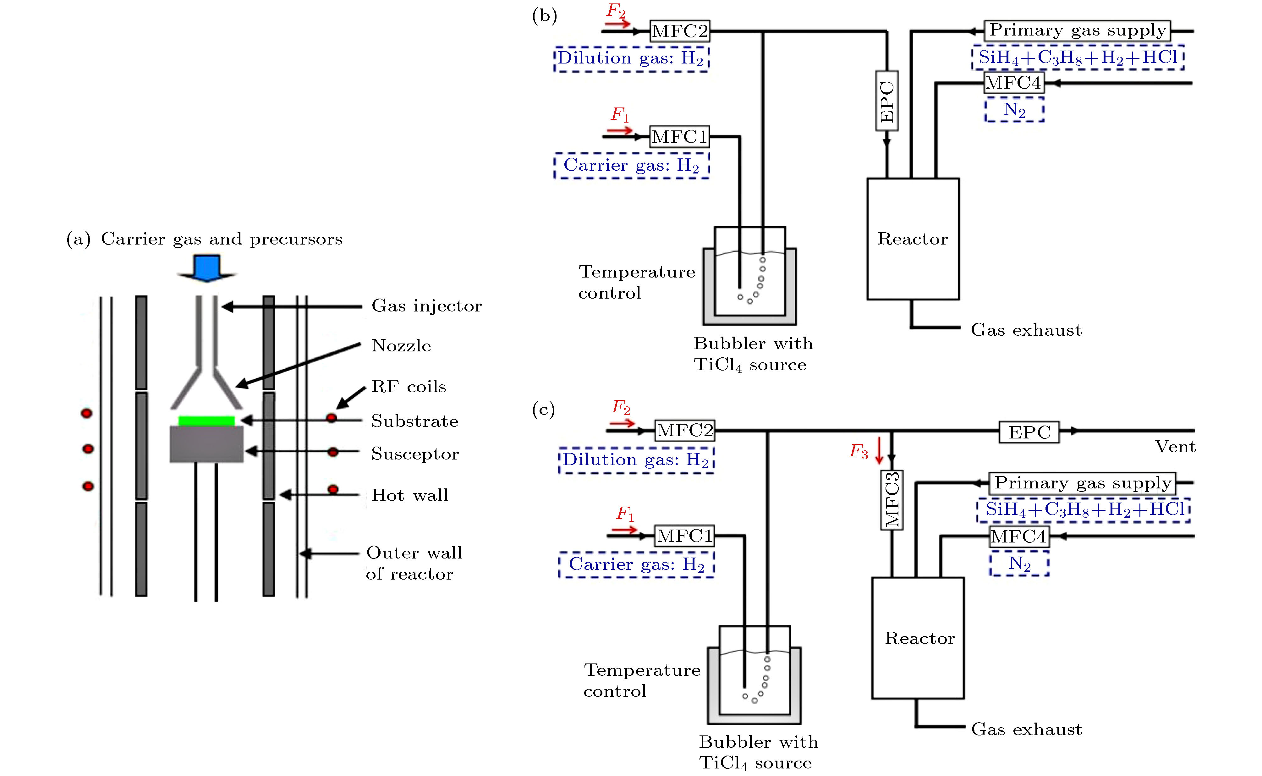
图 1 (a) 4H-SiC CVD外延设备示意图; Ti掺杂(b)单稀释和(c)双稀释管路示意图
Fig. 1. Schematics of (a) the CVD reactor for 4H-SiC epitaxial growth, (b) single-dilution pipe and (c) double-dilution pipe of TiCl4 gas delivery.
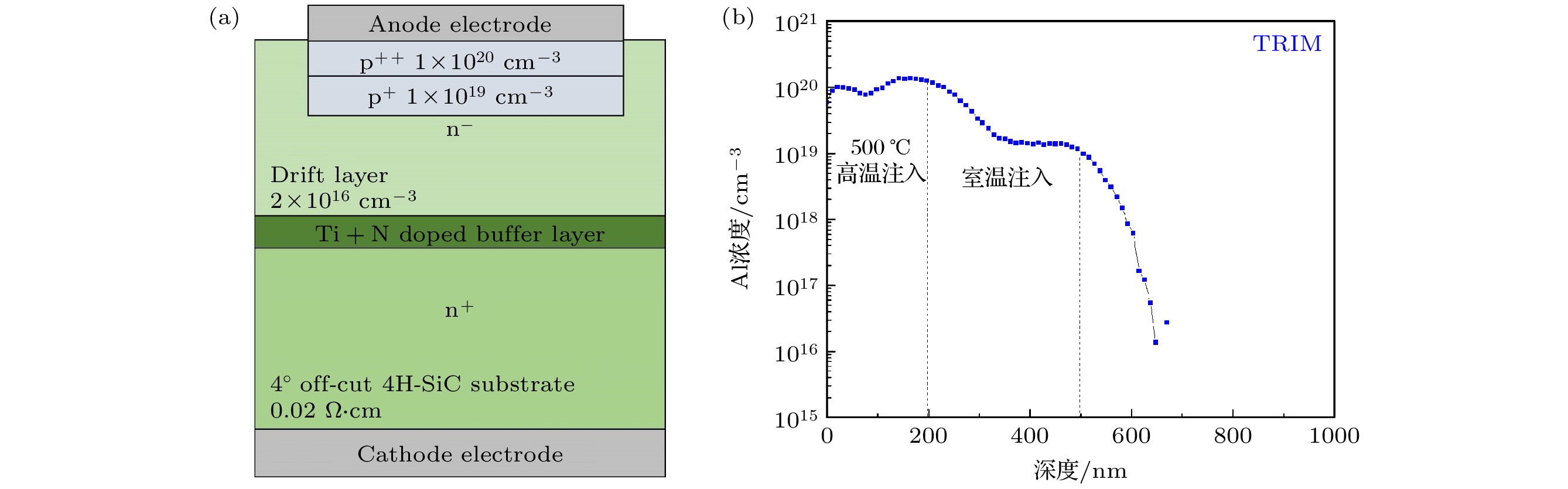
图 2 (a) 含Ti, N共掺杂缓冲层结构的SiC PiN二极管结构示意图; (b) TRIM模拟的Al注入浓度箱型分布
Fig. 2. (a) Schematic of the cross-sectional structure of a 4H-SiC PiN diode with Ti and N co-doped buffer layer; (b) box-profile of Al concentration by TRIM simulation.

图 3 Ti掺杂浓度随TiCl4摩尔流量的变化
Fig. 3. Relationship between Ti doping concentration and TiCl4 mole flow rate.
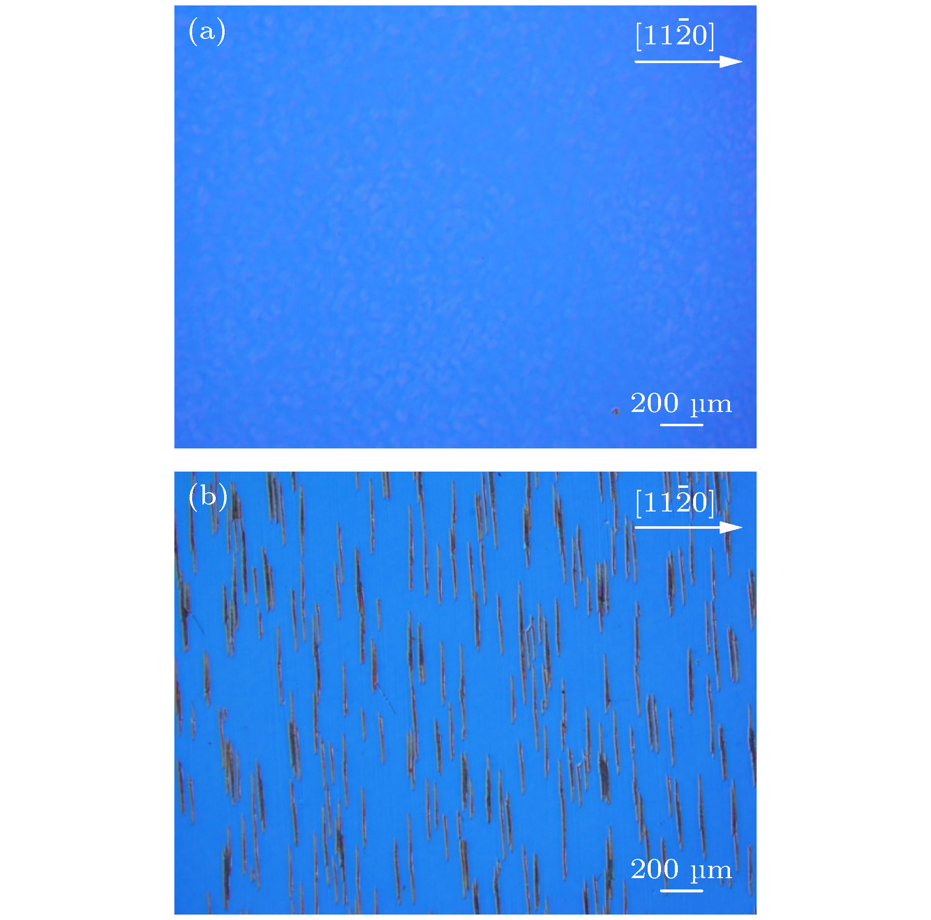
图 4 Ti, N共掺杂4H-SiC缓冲层表面形貌(Nd = 1.01 × 1019 cm–3) (a) Ti掺杂浓度为3.70 × 1015 cm–3; (b) Ti掺杂浓度为3.71 × 1016 cm–3
Fig. 4. Optical microscope images of the Ti and N co-doped 4H-SiC buffer layer surface with Ti doping concentrations of (a) 3.70 × 1015 cm–3 and (b) 3.71 × 1016 cm–3. Both with Nd = 1.01 × 1019 cm–3.

图 5 无缓冲层、仅含高浓度N掺杂缓冲层、含Ti和N共掺杂缓冲层的4H-SiC PiN二极管的正向特性 (a), (c), (e)在100 A/cm2电流密度下10 min, 正向压降随时间的变化; (b), (d), (f)正向偏置前后正向电流-电压曲线的对比
Fig. 5. (a), (c), (e) Change of forward voltage drop vs. time and (b), (d), (f) comparison between the forward I-V characteristics before and after being biased for 10 min at a current density of 100 A/cm2 for 4H-SiC PiN diodes without a buffer layer, with a highly N-doped buffer layer, and with a Ti and N co-doped buffer layer.
表 1 Ti掺杂实验参数
Table 1. Experimental parameters of Ti doping.
稀释管路 MFC1 MFC2 MFC3 TiCl4掺杂摩尔流量 /sccm /slm /sccm /(mol·min–1) 单稀释 1.25 9.800 — 7.25 × 10⁻⁷ 5 9.800 — 2.90 × 10⁻⁶ 50 9.800 — 2.90 × 10⁻⁵ 双稀释 50 0.100 5 8.95 × 10⁻⁷ 50 0.075 5 1.14 × 10⁻⁶ 50 0.040 5 1.62 × 10⁻⁶  下载: 导出CSV
-
[1] Lendenmann H, Dahlquist F, Johansson N, Soderholm R, Nilsson P A, Bergman J P, Skytt P 2001 Mater. Sci. Forum. 353–356 727
Google Scholar
[2] Skowronski M, Liu J Q, Vetter W M, Dudley M, Hallin C, Lendenmann H 2002 J. Appl. Phys. 92 4699
Google Scholar
[3] Caldwell J D, Stahlbush R E, Ancona M G, Glembocki O J, Hobart K D 2010 J. Appl. Phys. 108 044503
Google Scholar
[4] Maeda K, Hirano R, Sato Y, Tajima M 2012 Mater. Sci. Forum. 725 35
Google Scholar
[5] Ha S, Mieszkowski P, Skowronski M, Rowland L B 2002 J. Cryst. Growth 244 257
Google Scholar
[6] Tsuchida H, Kamata I, Miyazawa T, Ito M, Zhang X, Nagano M 2018 Mater. Sci. Semicond. Process. 78 2
Google Scholar
[7] Tanaka A, Matsuhata H, Kawabata N, Mori D, Inoue K, Ryo M, Fujimoto T, Tawara T, Miyazato M, Miyajima M, Fukuda K, Ohtsuki A, Tomohisa T, Tsuchida H, Yonezawa Y, Kimoto T 2016 J. Appl. Phys. 119 095711
Google Scholar
[8] Sumakeris J J, Bergman P, Das M K, Hallin C, Hull B A, Janzen E, Lendenmann H, O’Loughlin M J, Paisley M J, Ha S Y, Skowronski M, Palmour J W, Carter Jr C H 2006 Mater. Sci. Forum. 527-529 141
Google Scholar
[9] Hori T, Danno K, Kimoto T 2007 J. Cryst. Growth. 306 297
Google Scholar
[10] Stahlbush R E, VanMil B L, Myers Ward R L, Lew K K, Gaskill D K, Eddy Jr C R 2009 Appl. Phys. Lett. 94 041916
Google Scholar
[11] Mahadik N A, Stahlbush R E, Ancona M G, Lmhoff E A, Hobart K D, Myers-Ward R L, Eddy Jr C R, Gaskill D K, Kub F J 2012 Appl. Phys. Lett. 100 042102
Google Scholar
[12] Tawara T, Miyazawa T, Ryo M, Miyazato M, Fujimoto T, Takenaka K, Matsunaga S, Miyajima M, Otsuki A, Yonezawa Y, Kato T, Okumura H, Kimoto T, Tsuchida H 2016 J. Appl. Phys. 120 115101
Google Scholar
[13] Miyazawa T, Tawara T, Tsuchida H 2017 Mater. Sci. Forum. 897 67
Google Scholar
[14] Miyazawa T, Tawara T, Takanashi R, Tsuchida H 2016 Appl. Phys. Express 9 111301
Google Scholar
[15] Murata K, Tawara T, Yang A, Takanashi R, Miyazawa T, Tsuchida H 2019 J. Appl. Phys. 126 045711
Google Scholar
[16] Tawara T, Miyazawa T, Ryo M, Miyazato M, Fujimoto T, Takenaka K, Matsunaga S, Miyajima M, Otsuki A, Yonezawa Y, Kato T, Okumura H, Kimoto T, Tsuchida H 2017 Mater. Sci. Forum. 897 419
Google Scholar
[17] Dalibor T, Pensl G, Matsunami H, Kimoto T, Choyke W J, Schoner A, Nordell N 1997 Phys. Status Solidi A 162 199
Google Scholar
[18] Hobgood H M, Glass R C, Augustine G, Hopkins R H, Jenny J, Skowronski M, Mitchel W C, Roth M 1995 Appl. Phys. Lett. 66 1364
Google Scholar
[19] Dalibor T, Pensl G, Nordell N, Schoner A 1997 Phys. Rev. B 55 13618
Google Scholar
[20] Maier K, Muller H D, Schneider J 1992 Mater. Sci. Forum. 83–87 1183
Google Scholar

 下载:
下载:
计量
- 文章访问数: 10446
- PDF下载量: 145
- 被引次数: 0
