


-
现有计算机体系架构下的神经网络难以对多任务复杂数据进行高效处理, 成为制约人工智能技术发展的瓶颈之一, 而人脑的并行运算方式具有高效率、低功耗和存算一体的特点, 被视为打破传统冯·诺依曼计算体系最具潜力的运算体系. 突触仿生器件是指从硬件层面上实现人脑神经拟态的器件, 它可以模拟脑神经对信息的处理方式, 即“记忆”和“信息处理”过程在同一硬件上实现, 这对于构建新的运算体系具有重要的意义. 近年, 制备仿生突触器件的忆阻材料已获得进展, 但多聚焦于神经突触功能的模拟, 对于时空信息感知和传递的关键研究较为缺乏. 本文通过制备一种双层结构忆阻器, 实现了突触仿生器件的基本功能包括双脉冲易化和抑制、脉冲时间依赖突触可塑性(spiking time dependent plasticity, STDP)和经验式学习等, 还对器件的信息感知、传递特性和稳定性进行了研究, 发现该器件脉冲测试结果满足神经网络处理时空信息的基本要求, 这一结果可以为忆阻器在类脑芯片中的应用提供参考.
-
关键词:
- 双层结构忆阻器 /
- 神经网络 /
- 脉冲时间依赖突触可塑性 /
- 时空信号处理
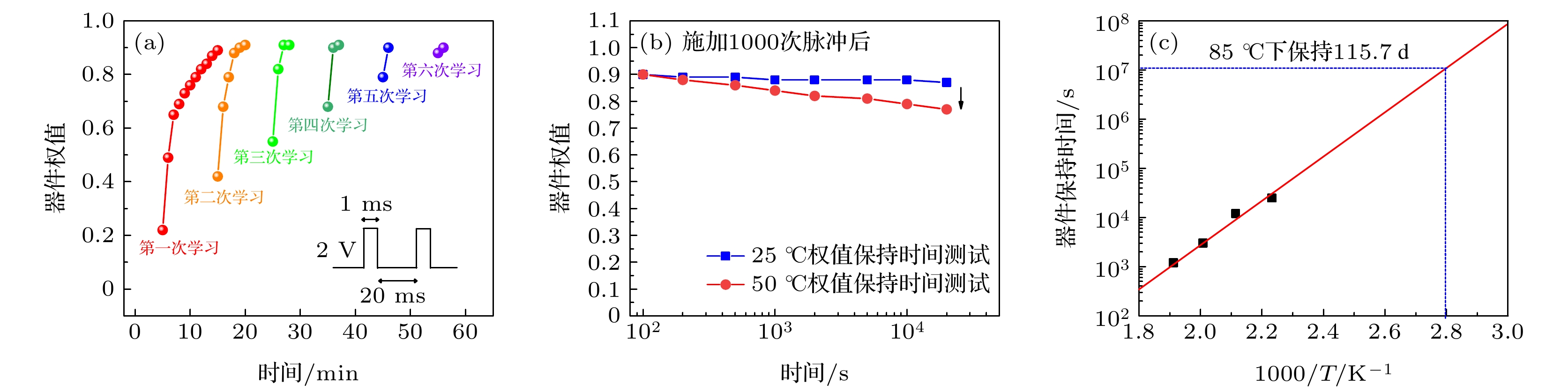
The neural network under the current computer architecture is difficult to process complex data efficiently, thus becoming one of the bottlenecks restricting the development of artificial intelligence technology. The human brain has the characteristics of high efficiency, low power consumption and integration of memory and computing, and is regarded as a most potential computing system to break the traditional von Neumann computing system. Synaptic biomimetic device is to realize the neural mimicry of human brain from the hardware level. It can simulate the information processing mode of brain nerve, that is, the process of “memory” and “calculation” can be realized on the same device, which is of great significance in building a new computing system. In recent years, the fabrication of memristor materials for bio-mimetic synaptic devices has made progress, but most of them focus on the simulation of synaptic function. The key research of pulse signal perception and information transmission is relatively lacking. In this paper, an bi-layer memristor with structure Al/nc-Al AlN/A2O3/Ag is fabricated by rf sputtering method to realize the basic functions of bionic synaptic devices. It is found that this bio-mimetic memristor exhibits bipolar switching property which is the basic condition to produce memristor based neural synapse. Both of PPF and PPD process can be observed and there will be no firing signal observed if the pulse interval is as large as 350 ms. The change of device conductance should be related to pulse voltage, frequency and pulse number applied. The larger pulse voltage, frequency and number will cause device conductance to increase sharply in both positive and negative pulse voltage region. The STDP measurement is executed with different sequence pulses from post and previous neuron separately. If the pulse of previous synapse comes in front of pulse from post synapse, the conductance will increase, which is so-called LTP process. If the pulse of previous neuron comes behind of pulse from post neuron, the conductance will be reduced as well. Triplet STDP measurement is executed with at least three pulses from previous and post neuron at the meanwhile. It is concluded that if the interval time of the first two pulses is fixed, the device conductance more depends on the value of the second and third pulse interval. Ebbinghaus forgetting curve can be used to explain the reason why the device conductance declines with time going by. The stability study of this memristor includes endurance and retention properties at both room and high temperature. It is found this biomimetic memristor can maintain its conductance for over 115.7 days at 85 ℃, which is long enough for current neural network design.-
Keywords:
- bi-layer memristor /
- neural network /
- spiking time dependent plasticity /
- spatiotemporal signal processing
[1] Pei J, Deng L, Song S, et al. 2019 Nature 572 106
 Google Scholar
[2] Krestinskaya O, Salama K N, James A P 2020 Adv. Intell. Syst. 2 2000075
Google Scholar
[3] Shastri B J, Tait A N, Ferreira L T, Pernice W H P, Bhaskaran H, Wright C D, Prucnal P R 2021 Nat. Photonics 15 102
Google Scholar
[4] Abrol A, Fu Z, Salman M, Silva R, Du Y, Plis S, Calhoun V 2021 Nat. Commun. 12 353
Google Scholar
[5] Xia Q F, Yang J J, Publisher C 2019 Nat. Mater. 18 518
Google Scholar
[6] Lim D H, Wu S, Zhao R, Lee J H, Jeong H, Shi L 2021 Nat. Commun. 12 319
Google Scholar
[7] Demin V A, Nekhaev D V, Surazhevsky I A, Nikiruy K E, Emelyanov A V, Nikolaev S N, Rylkov V V, Kovalchuk M V 2021 Neural Networks 134 64
Google Scholar
[8] Irem B, Manuel L G, Nandakumar S R, Timoleon M, Thomas P, Tomas T, Bipin R, Yusuf L, Abu S, Evangelos E 2018 Nat. Commun. 9 25141
[9] Wang Z Q, Xu H Y, Li X H, Yu H, Liu Y C, Zhu X J 2012 Adv. Funct. Mater. 22 2758
Google Scholar
[10] Zhang Y N, Tang J S, Li X Y, Gao B, He Q, Wu H Q 2021 Nat. Commun. 12 408
Google Scholar
[11] Liu L F, Yu D, Ma W J, Chen B, Zhang F F, Gao B, Kang J F 2015 Jpn. J Appl Phys 54 021802
Google Scholar
[12] Chen C, Yang Y C, Zeng F, Pan F 2010 Appl. Phys. Lett. 97 083502
Google Scholar
[13] Zhu W, Chen T P, Yang M, Liu Y, Fung S 2012 IEEE Trans. Electron Devices 59 2363
[14] Zhao B, Xiao M, Zhou Y N 2019 Nanotechnology 30 425202
Google Scholar
[15] Gul F, Efeoglu H 2017 Ceram. Int. 43 10770
Google Scholar
[16] Bae S H, Lee S, Koo H, Lin L, Jo B H, Park C, Wang Z L 2013 Adv. Mater. 25 5098
Google Scholar
[17] Rodriguez F A, Cagli C, Perniola L, Miranda E, Sune J 2018 Microelectron. Eng. 195 101
Google Scholar
[18] Krishna K P, Dhanashri V D, Shraddha M B, Harshada S P, Suraj M M, Ajay S N, Sawanta S M, Chang K H, Sungjun K, Pramod S P, Tukaram D D 2019 J. Phys. D: Appl. Phys 52 175306
Google Scholar
[19] 陈义豪, 徐威, 王钰琪, 万相, 李岳峰, 梁定康, 陆立群, 刘鑫伟, 连晓娟, 胡二涛, 郭宇峰, 许剑光, 童祎, 肖建 2019 物理学报 68 098501
Google Scholar
Chen Y H, Xue W, Wang Y Q, Wan X, Li Y F, Liang D K, Lu L Q, Liu X W, Lian X J, Hu E T, Guo Y F, Xu J G, Tong Y, Xiao J 2019 Acta Phys. Sin 68 098501
Google Scholar
[20] Sahu D P, Jetty P, Jammalamadaka S N 2020 Nanotechnology 32 155701
[21] Fyrigos I A, Ntinas V, Sirakoulis G C, Dimitrakis P, Karafyllidis I G 2021 IEEE Trans Nanotechnol. 20 113
Google Scholar
[22] Bai N, Tian B Y, Miao G Q, Xue K H, Wang T, Yuan J H, Liu X X, Li Z N, Guo S, Zhou Z P, Liu N, Lu H, Tang X D, Sun H J, Miao X S 2021 Appl. Phys. Lett. 118 043502
Google Scholar
[23] Yoon J H, Wang Z, Kim K M, Wu H, Ravichandran V, Xia Q, Hwang C S, Yang J J 2018 Nat. Commun. 9 417
Google Scholar
[24] Jiang H, Belkin D, Savelev S E, Wang Z R, Li Y N, Joshi S, Midya R, Li C, Rao M Y, Barnell M, Wu Q, Yang J J, Xia Q F 2017 Nat. Commun. 8 882
Google Scholar
[25] Zhu W, Chen T P, Liu Y, Sun F 2012 J. Appl. Phys. 112 063706
Google Scholar
[26] Zhu W, Chen T P, Liu Z, Yang M, Liu Y, Sun F 2009 J. Appl. Phys. 106 093706
Google Scholar
[27] Zhang X, Wang W, Liu Q, Zhao X, Wei J, Cao R, Yao Z, Zhu X, Zhang F, Lü H 2018 IEEE Electron Device Lett. 39 308
Google Scholar
[28] Chen Y, Wang Y, Luo Y, Liu X, Tong Y 2019 IEEE Electron Device Lett. 40 1686
Google Scholar
[29] Jo S H, Chang T, Idongesit E, Bhavitavya B B, Pinaki M, Wei L 2010 Nano Lett. 10 1297
Google Scholar
[30] Wang Z R, Joshi S, , Savel’ev S E, Jiang H, Midya R, Lin P, Hu M, Ge N, Strachan J P, Li Z Y, Wu Q, Barne M, Li G L, Xin H L, Williams R S, Xia Q F, Yang J J 2017 Nat. Mater. 16 101
Google Scholar
[31] Pan X, Zheng Y, Shi Y M, Chen W 2021 ACS Materials lett. 3 235
Google Scholar
[32] 张晨曦, 陈艳, 仪明东, 朱颖, 李腾飞, 刘露涛, 王来源, 解令海, 黄维 2018 中国科学: 信息科学 48 115
Google Scholar
Zhang C X, Chen Y, Yi D M, Zhu Y, Li T F, Liu L T, Wang L Y, Xie L H, Huang W 2018 Sci. Sin. Informationis 48 115
Google Scholar
[33] Neeraj P, Bipin R, Udayan G 2017 IEEE Electron Device Lett. 38 740
Google Scholar
[34] Cai W R, Frank E, Ronald T 2015 IEEE Trans. Biomed. Circuits. Syst. 9 87
Google Scholar
[35] Yang R, Huang H M, Hong Q H, Yin X B, Tan Z H, Shi T, Zhou Y X, Miao X S, Wang X P, Mi S B, Jia C L, Guo X 2018 Adv. Funct. Mater. 28 1704455
Google Scholar
[36] Rubin D C, Wenzel A E 1996 Psychol. Rev. 103 734
Google Scholar
-
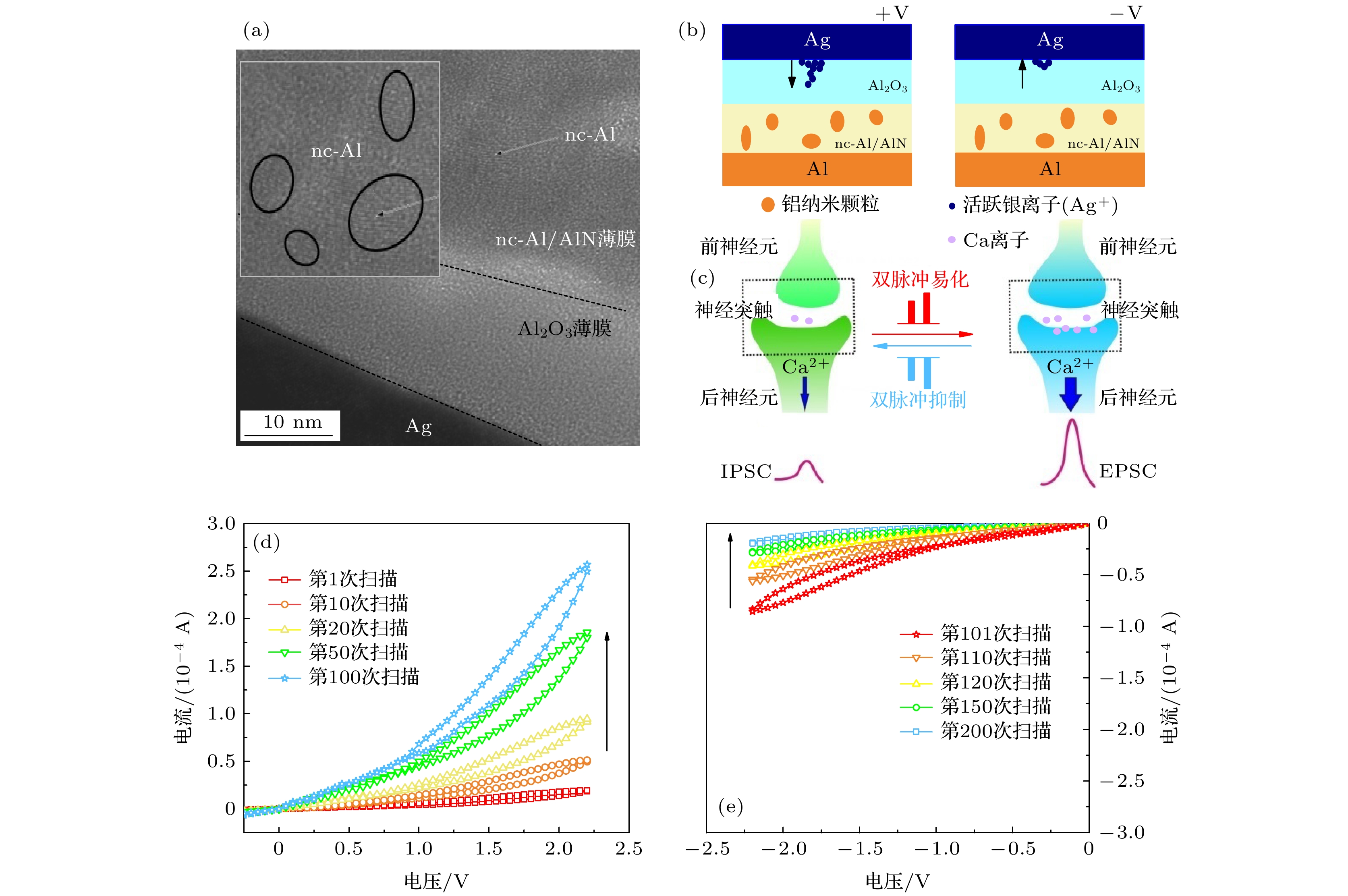
图 1 (a) 器件TEM图; (b) 器件结构图; (c) 神经突触工作原理; (d) 连续100次正向电压扫描测试; (e) 连续100次负向电压扫描测试
Fig. 1. (a) TEM result of bi-layer memristor; (b) structure of memristor; (c) mechanisms of synapse working; (d) continued positive I-V biasing with 100 times; (e) continued negative I-V biasing with another 100 times.
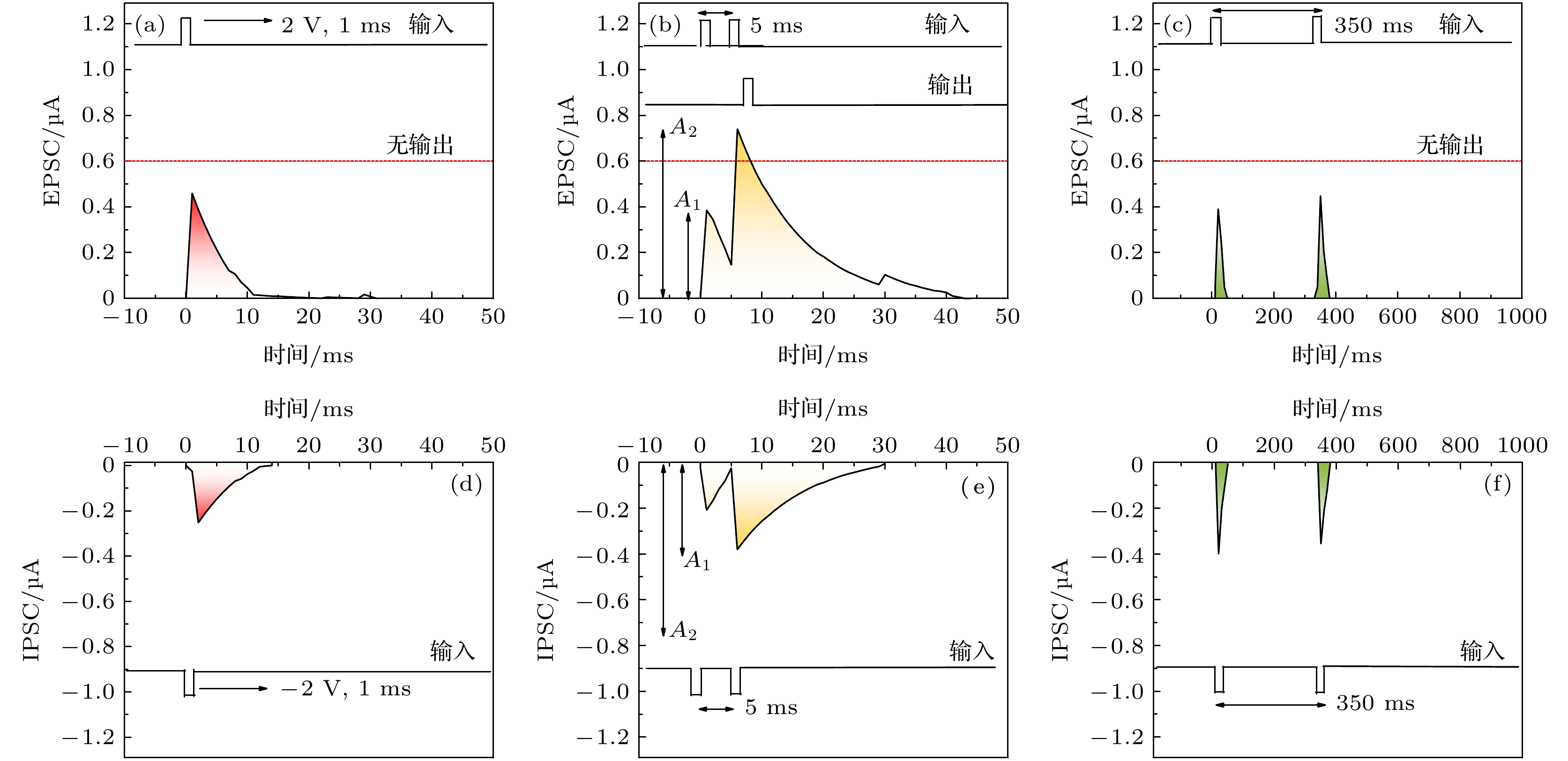
图 2 器件内EPSC和IPSC的脉冲测 (a) 施加单个正向脉冲的EPSC; (b) 双脉冲易化的EPSC; (c) 施加双正向脉冲但间隔时间350 ms的EPSC; (d) 施加单个负向脉冲的IPSC; (e) 双脉冲抑制的IPSC; (f) 施加双负向脉冲但间隔时间350 ms的IPSC
Fig. 2. Pulse voltage measurement of memristor: (a) EPSC with single positive pulse applied; (b) EPSC of PPF; (c) two positive pulses applied with 350 ms interval; (d) EPSC with single negative pulse applied; (e) IPSC of PPD; (f) two negative pulses applied with 350 ms interval.

图 3 (a) 以100 Hz频率施加幅值和宽度为2 V和5 ms的正向脉冲, 器件权值随时间增加; (b) 以100 Hz频率施加幅值和宽度为–2 V和5 ms的负向脉冲, 器件权值随时间减小; (c) 以2 Hz频率施加幅值和宽度为2 V和5 ms的正向脉冲, 器件权值也会随时间减小
Fig. 3. (a) Device conductance increased with 100 Hz, 2 V in amplitude and 5 ms in width positive voltage pulse applied; (b) device conductance decreased with 100 Hz, -2 V in amplitude and 5 ms in width positive voltage pulse applied; (c) device conductance will decrease with 2 Hz, 2 V in amplitude and 5 ms in width positive voltage pulse applied.
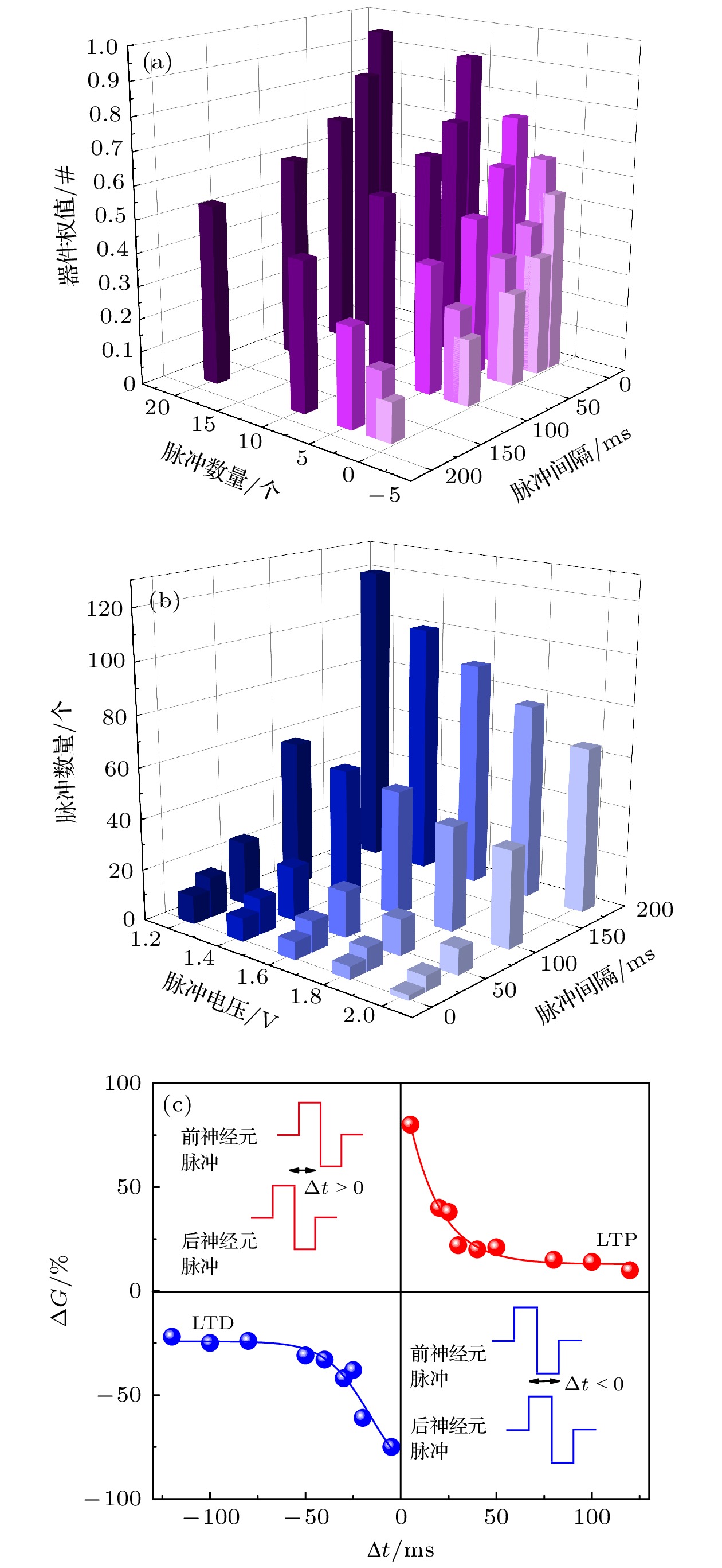
图 4 (a) 器件权值与施加脉冲数量和脉冲间隔的关系; (b) 器件达到最大权值所需脉冲数量与脉冲电压和间隔的关系; (c) STDP特性
Fig. 4. (a) The relationship of device conductance with pulse number and interval; (b) the pulse number needed to make device conductance maximized with different pulse voltage and interval; (c) STDP.
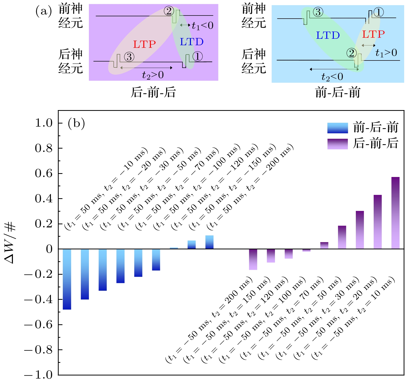
图 5 (a) 后-前-后和前-后-前时序的神经元信号; (b) 三脉冲STDP器件权值的变化
Fig. 5. (a) Singal with post-pre-post and pre-post-pre sequence; (b) triplet-STDP.
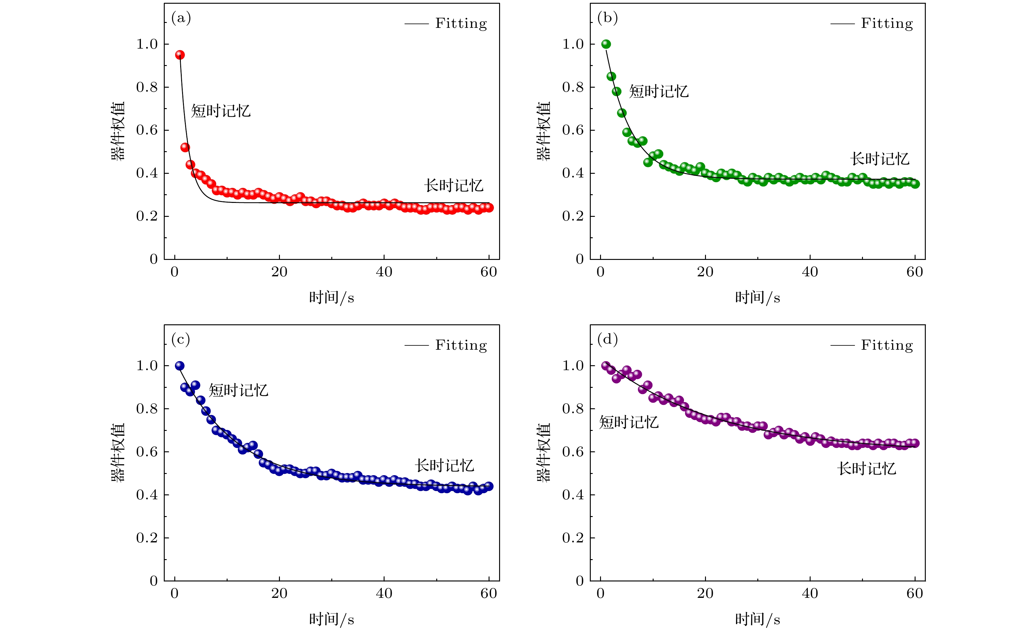
图 6 分别施加10个(a), 50个(b), 100个(c)和200个(d) 幅值为1.2 V、宽度为5 ms的脉冲电压后器件权值随时间减弱的特性
Fig. 6. The device conductance changed with time after applied (a) 10, (b) 50, (c) 100 and (d) 200 positive voltage pulses with the amplitude of 1.2 V and pulse width of 5 ms.
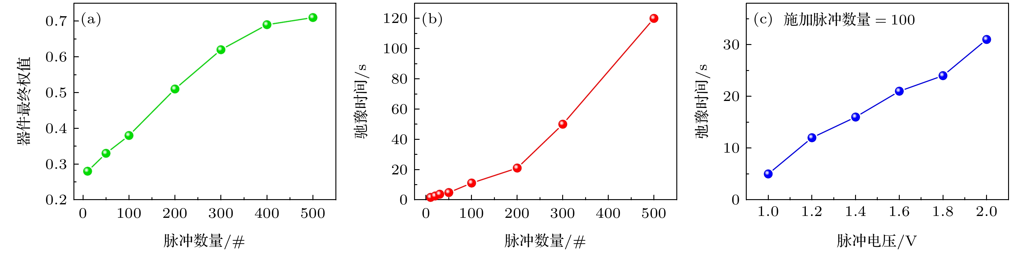
图 7 (a) 器件最终权值与施加脉冲数量的关系; (b) 器件弛豫时间与施加脉冲数量的关系; (c) 器件弛豫时间与施加脉冲电压的关系
Fig. 7. (a) The relationship between device conductance and applied pulse number; (b) the relationship between device relaxation time and applied pulse number; (c) the relationship between device relaxation time and applied pulse voltage.
-
[1] Pei J, Deng L, Song S, et al. 2019 Nature 572 106
Google Scholar
[2] Krestinskaya O, Salama K N, James A P 2020 Adv. Intell. Syst. 2 2000075
Google Scholar
[3] Shastri B J, Tait A N, Ferreira L T, Pernice W H P, Bhaskaran H, Wright C D, Prucnal P R 2021 Nat. Photonics 15 102
Google Scholar
[4] Abrol A, Fu Z, Salman M, Silva R, Du Y, Plis S, Calhoun V 2021 Nat. Commun. 12 353
Google Scholar
[5] Xia Q F, Yang J J, Publisher C 2019 Nat. Mater. 18 518
Google Scholar
[6] Lim D H, Wu S, Zhao R, Lee J H, Jeong H, Shi L 2021 Nat. Commun. 12 319
Google Scholar
[7] Demin V A, Nekhaev D V, Surazhevsky I A, Nikiruy K E, Emelyanov A V, Nikolaev S N, Rylkov V V, Kovalchuk M V 2021 Neural Networks 134 64
Google Scholar
[8] Irem B, Manuel L G, Nandakumar S R, Timoleon M, Thomas P, Tomas T, Bipin R, Yusuf L, Abu S, Evangelos E 2018 Nat. Commun. 9 25141
[9] Wang Z Q, Xu H Y, Li X H, Yu H, Liu Y C, Zhu X J 2012 Adv. Funct. Mater. 22 2758
Google Scholar
[10] Zhang Y N, Tang J S, Li X Y, Gao B, He Q, Wu H Q 2021 Nat. Commun. 12 408
Google Scholar
[11] Liu L F, Yu D, Ma W J, Chen B, Zhang F F, Gao B, Kang J F 2015 Jpn. J Appl Phys 54 021802
Google Scholar
[12] Chen C, Yang Y C, Zeng F, Pan F 2010 Appl. Phys. Lett. 97 083502
Google Scholar
[13] Zhu W, Chen T P, Yang M, Liu Y, Fung S 2012 IEEE Trans. Electron Devices 59 2363
[14] Zhao B, Xiao M, Zhou Y N 2019 Nanotechnology 30 425202
Google Scholar
[15] Gul F, Efeoglu H 2017 Ceram. Int. 43 10770
Google Scholar
[16] Bae S H, Lee S, Koo H, Lin L, Jo B H, Park C, Wang Z L 2013 Adv. Mater. 25 5098
Google Scholar
[17] Rodriguez F A, Cagli C, Perniola L, Miranda E, Sune J 2018 Microelectron. Eng. 195 101
Google Scholar
[18] Krishna K P, Dhanashri V D, Shraddha M B, Harshada S P, Suraj M M, Ajay S N, Sawanta S M, Chang K H, Sungjun K, Pramod S P, Tukaram D D 2019 J. Phys. D: Appl. Phys 52 175306
Google Scholar
[19] 陈义豪, 徐威, 王钰琪, 万相, 李岳峰, 梁定康, 陆立群, 刘鑫伟, 连晓娟, 胡二涛, 郭宇峰, 许剑光, 童祎, 肖建 2019 物理学报 68 098501
Google Scholar
Chen Y H, Xue W, Wang Y Q, Wan X, Li Y F, Liang D K, Lu L Q, Liu X W, Lian X J, Hu E T, Guo Y F, Xu J G, Tong Y, Xiao J 2019 Acta Phys. Sin 68 098501
Google Scholar
[20] Sahu D P, Jetty P, Jammalamadaka S N 2020 Nanotechnology 32 155701
[21] Fyrigos I A, Ntinas V, Sirakoulis G C, Dimitrakis P, Karafyllidis I G 2021 IEEE Trans Nanotechnol. 20 113
Google Scholar
[22] Bai N, Tian B Y, Miao G Q, Xue K H, Wang T, Yuan J H, Liu X X, Li Z N, Guo S, Zhou Z P, Liu N, Lu H, Tang X D, Sun H J, Miao X S 2021 Appl. Phys. Lett. 118 043502
Google Scholar
[23] Yoon J H, Wang Z, Kim K M, Wu H, Ravichandran V, Xia Q, Hwang C S, Yang J J 2018 Nat. Commun. 9 417
Google Scholar
[24] Jiang H, Belkin D, Savelev S E, Wang Z R, Li Y N, Joshi S, Midya R, Li C, Rao M Y, Barnell M, Wu Q, Yang J J, Xia Q F 2017 Nat. Commun. 8 882
Google Scholar
[25] Zhu W, Chen T P, Liu Y, Sun F 2012 J. Appl. Phys. 112 063706
Google Scholar
[26] Zhu W, Chen T P, Liu Z, Yang M, Liu Y, Sun F 2009 J. Appl. Phys. 106 093706
Google Scholar
[27] Zhang X, Wang W, Liu Q, Zhao X, Wei J, Cao R, Yao Z, Zhu X, Zhang F, Lü H 2018 IEEE Electron Device Lett. 39 308
Google Scholar
[28] Chen Y, Wang Y, Luo Y, Liu X, Tong Y 2019 IEEE Electron Device Lett. 40 1686
Google Scholar
[29] Jo S H, Chang T, Idongesit E, Bhavitavya B B, Pinaki M, Wei L 2010 Nano Lett. 10 1297
Google Scholar
[30] Wang Z R, Joshi S, , Savel’ev S E, Jiang H, Midya R, Lin P, Hu M, Ge N, Strachan J P, Li Z Y, Wu Q, Barne M, Li G L, Xin H L, Williams R S, Xia Q F, Yang J J 2017 Nat. Mater. 16 101
Google Scholar
[31] Pan X, Zheng Y, Shi Y M, Chen W 2021 ACS Materials lett. 3 235
Google Scholar
[32] 张晨曦, 陈艳, 仪明东, 朱颖, 李腾飞, 刘露涛, 王来源, 解令海, 黄维 2018 中国科学: 信息科学 48 115
Google Scholar
Zhang C X, Chen Y, Yi D M, Zhu Y, Li T F, Liu L T, Wang L Y, Xie L H, Huang W 2018 Sci. Sin. Informationis 48 115
Google Scholar
[33] Neeraj P, Bipin R, Udayan G 2017 IEEE Electron Device Lett. 38 740
Google Scholar
[34] Cai W R, Frank E, Ronald T 2015 IEEE Trans. Biomed. Circuits. Syst. 9 87
Google Scholar
[35] Yang R, Huang H M, Hong Q H, Yin X B, Tan Z H, Shi T, Zhou Y X, Miao X S, Wang X P, Mi S B, Jia C L, Guo X 2018 Adv. Funct. Mater. 28 1704455
Google Scholar
[36] Rubin D C, Wenzel A E 1996 Psychol. Rev. 103 734
Google Scholar

 下载:
下载:
计量
- 文章访问数: 9131
- PDF下载量: 200
- 被引次数: 0
