


-
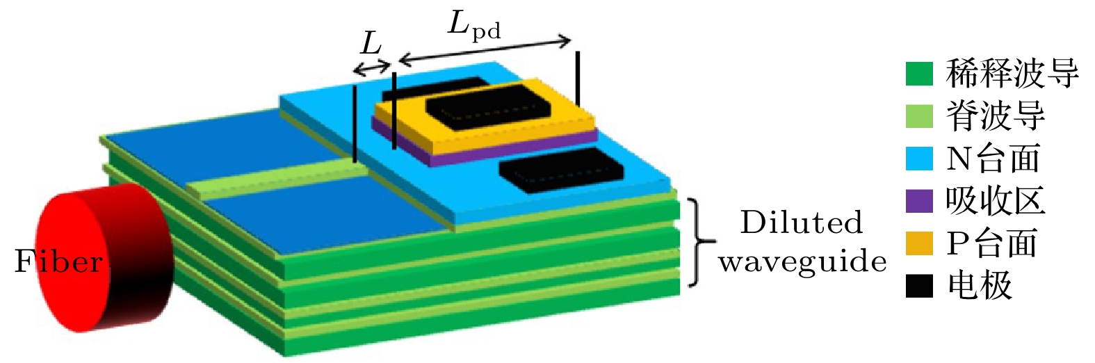
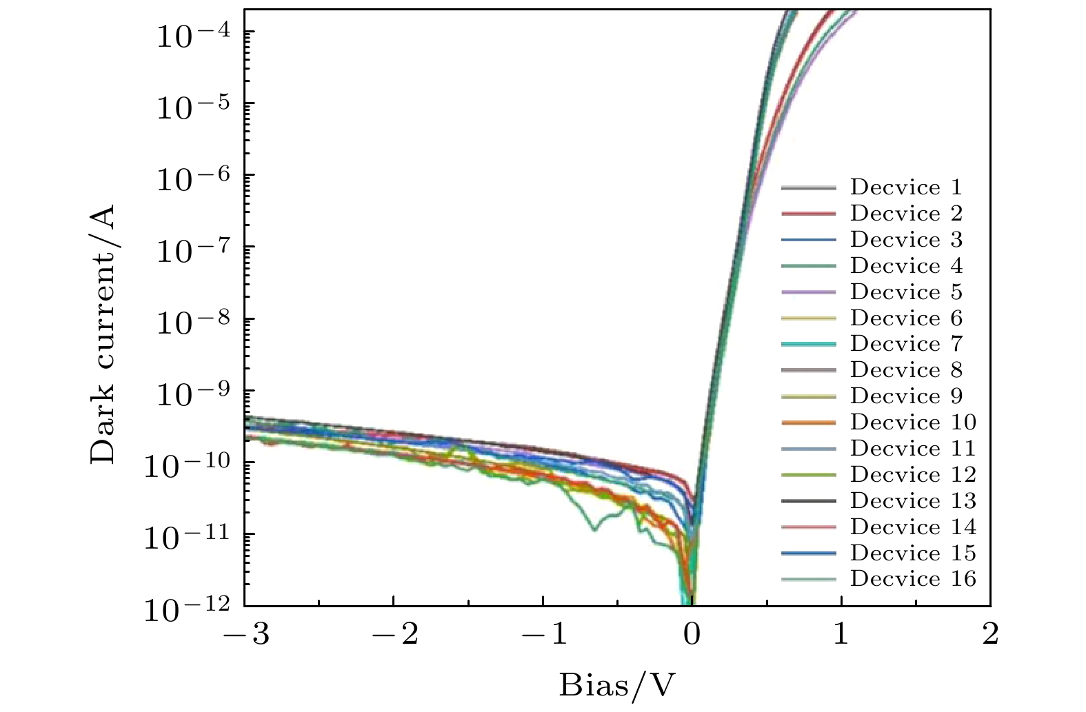
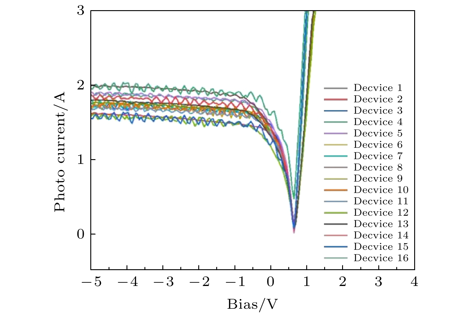
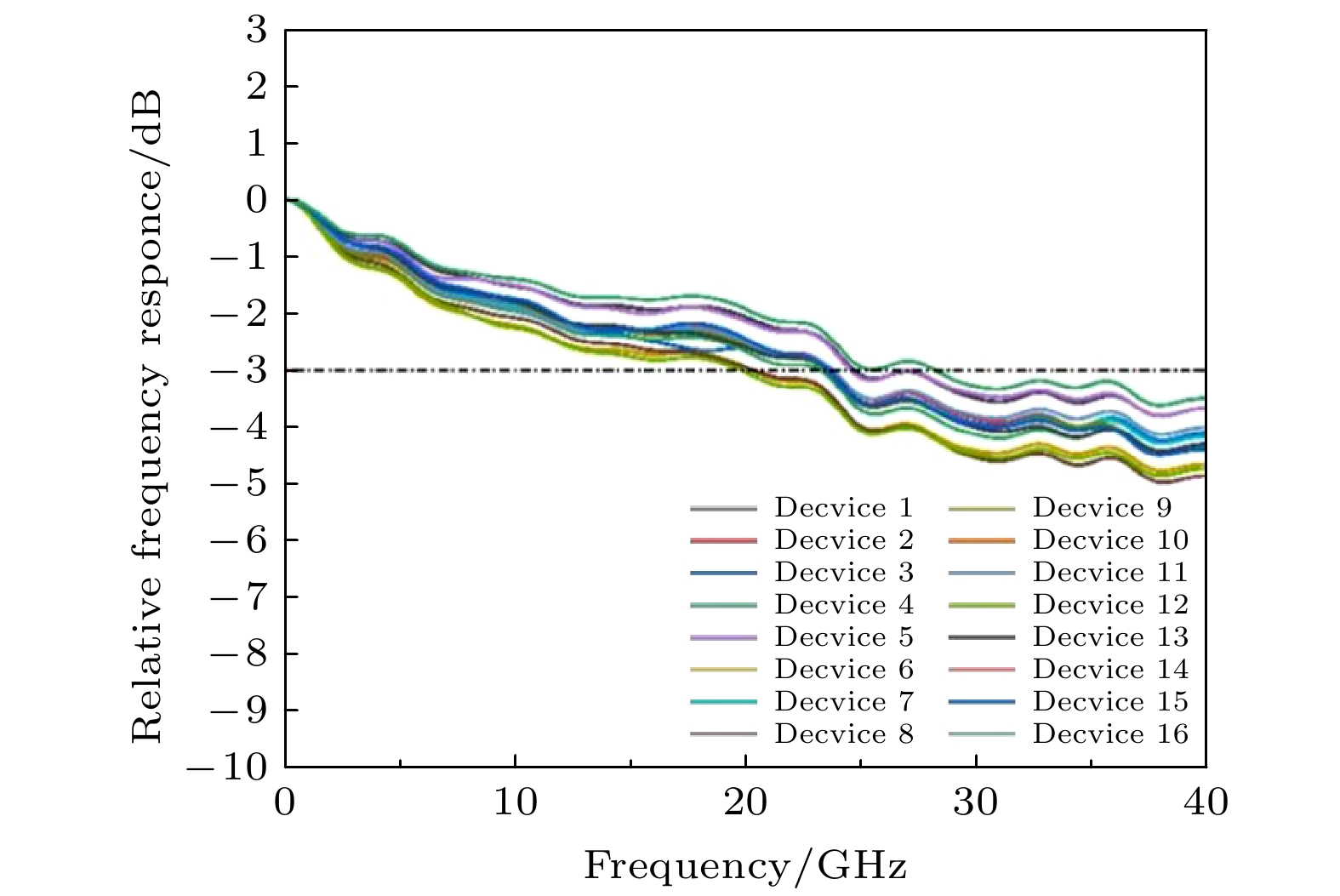
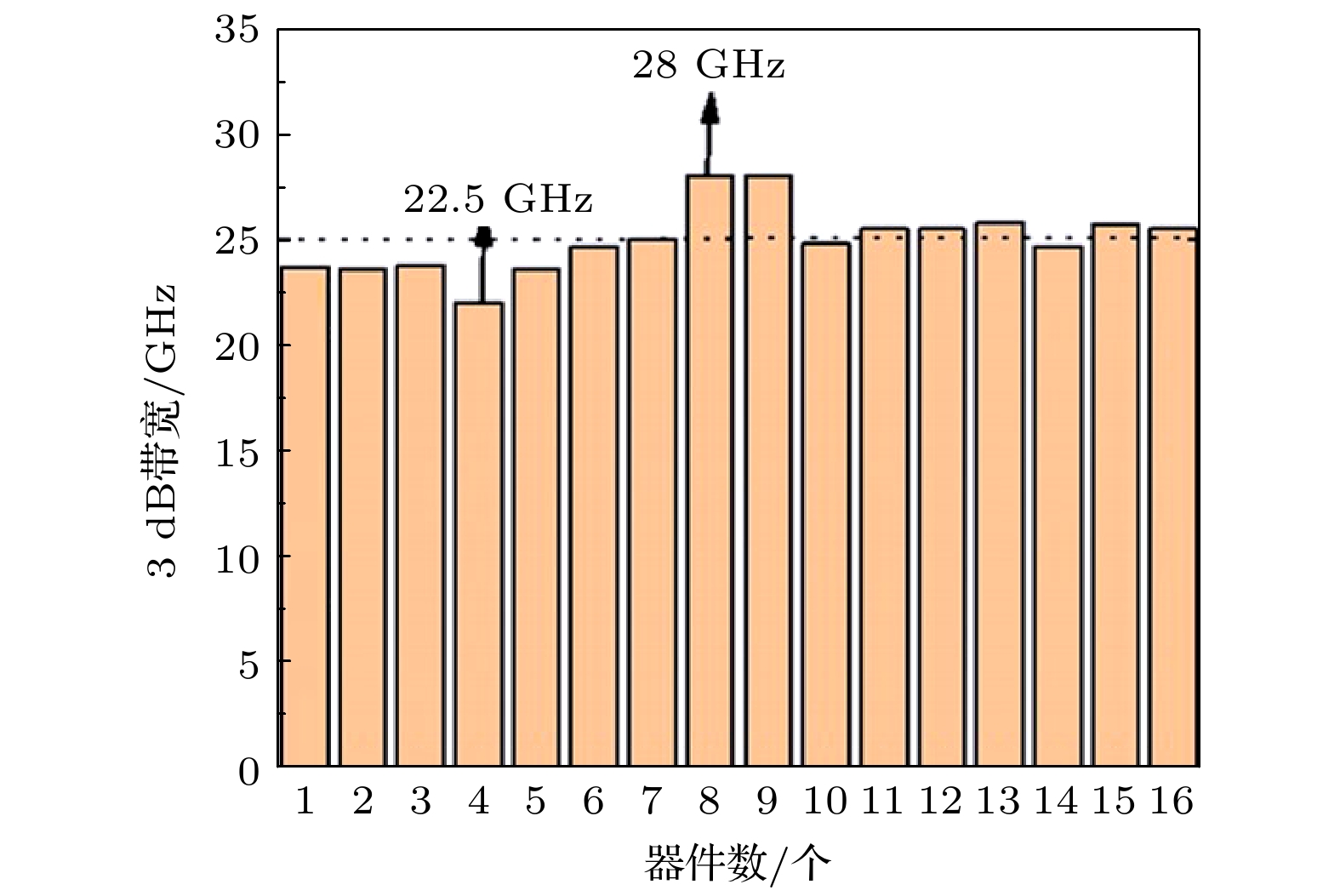
相较于面入射型和边入射型光电探测器, 倏逝波耦合型光电探测器(evanescent coupling photodetector, ECPD)能够同时具备高带宽和高量子效率, 因此在高速光通信领域有着广袤的应用前景. ECPD由稀释波导、单模脊波导和PIN光电二极管组成, 通过倏逝波定向耦合提高光纤入射光到探测器吸收芯层的耦合效率. 本文详细介绍了一种铟磷基ECPD阵列的结构设计、实验制备和测试结果. 测试结果表明, 制备的ECPD暗电流较低, 在–3和0 V外加偏压下探测器暗电流低至215和1.23 pA. 在有源区面积为5 μm × 20 μm的情况下, 器件仍能有较高响应度, 为0.5 A/W (无增透膜). 对探测器进行高频性能测试, 探测器阵列的所有探测器带宽均超过25 GHz, 总带宽400 GHz, 可以集成任意光学器件.Compared with surface and edge incident photodetectors, evanescent coupling photodetector (ECPD) has high bandwidth and high quantum efficiency, so it has a broad application prospect in the field of high-speed optical communication. The evanescent wave coupled photodetector is composed of a diluted waveguide, a single-mode ridge waveguide and a PIN photodiode. By directional evanescent wave coupling, the coupling efficiency of the incident light from the fiber to the absorption core of the photodetector is improved. In this paper, the structure design, experimental preparation and test results of an indium phosphorus based evanescent wave coupled photodetector array are introduced in detail. The test results show that the dark current of the evanescent wave coupled photodetector array is as low as 215 pA and 1.23 pA under –3 and 0 V bias, respectively. When the active area is 5 μm × 20 μm, the device still has a high responsivity of 0.5 A/W (without antireflection film). The high frequency performance of the detector is tested. The bandwidth of each detector is more than 25 GHz, and the total bandwidth is more than 400 GHz. Any optical device can be integrated. The detector array can be applied to the WDM receiving system of 400 Gbit/s and coherent receiving system of 200 Gbit/s.
-
Keywords:
- evanescent wave coupling /
- pin detector array /
- low dark current /
- 400 GHz
[1] Poon W A, Luo X, Xu F, Chen H 2009 IEEE J. Proc. 97 1216
 Google Scholar
[2] Lira H L R, Manipatruni S, Lipson M 2009 IEEE J. Opt. Express 17 22271
Google Scholar
[3] Xu Q, Schmidt B, Shakya J, Lipson M 2006 Opt. Express 14 9431
Google Scholar
[4] Bosco G, Curri V, Carena A, Poggiolini P, Forghieri F 2011 J. Lightwave Technol. 29 53
Google Scholar
[5] 喻松, 张华, 申静, 张永军, 顾畹仪 2008 物理学报 57 909
Google Scholar
Yu S, Zhang H, Shen J, Zhang Y J, Gu W Y 2008 Acta Phys. Sin. 57 909
Google Scholar
[6] 万峰, 武保剑, 曹亚敏, 王瑜浩, 文峰, 邱昆 2019 物理学报 68 114207
Google Scholar
Wang F, Wu B J, Cao Y M, Wang Y H, Wen F, Qiu K 2019 Acta Phys. Sin. 68 114207
Google Scholar
[7] Heck M J R, Bauters J F, Davenport, M L, Doylend J K 2013 IEEE J. Sel. Top. Quantum Electron. 19 6100117
Google Scholar
[8] Huang B, Xu Z, Wei W, Zan D, Ning G, Zhang Z, Chen H 2011 Opt. Commun. 284 3924
Google Scholar
[9] Kwack M J, Tanemura T, Higo A, Nakano Y 2012 Opt. Express 20 28734
Google Scholar
[10] Zhang X L, Liu S T, Lu D, Zhang R K, Ji C 2015 Chin. Phys. Lett. 32 054202
[11] Nagarajan R, Joyner C H, Schneider R P 2005 IEEE J. Sel. Top. Quantum Electron. 11 50
Google Scholar
[12] ShengZ, Liu L, Joost B, He S L, Dries V T 2010 Opt. Express 18 1756
Google Scholar
[13] Kato K, Hata S, Kozen A, Yoshida J I, Kawano K 1991 J. IEEE Photonics Technol. Lett. 3 473
Google Scholar
[14] Ohnaka K, Inoue U T, Hasegawa H N, Serizawa H 1985 IEEE J. Quantum Electron. 21 1236
Google Scholar
[15] Demiguel S, Li N, Li X W, Zheng X G, Kim J, Champbell J C, Lu H F, Anselm A 2003 IEEE Photonics Technol. Lett. 15 1761
[16] Liu S Q, Yang X H, Liu Y, Li B, Han Q 2013 Chin. Phys. B 22 108503
Google Scholar
[17] Giraudet L, Banfi F, Demiguel S, Herve-Gruyer G 1999 IEEE Photonics Technol. Lett. 11 111
[18] Magnin V, Giraudet L, Harari J, Decobert J, Pagnot P, Boucherez E, Decoster D 2002 J. Lightwave Technol. 20 477
Google Scholar
[19] Yang C D, Lei P H, Pong D J, Wu M Y, Ho C L, Ho W J 2004 IEEE J. Quantum Electron. 40 1607
Google Scholar
[20] Wang Y S, Chang S J, Chiou Y Z, Lin W 2009 J. Electrochem. Soc. 155 307
-
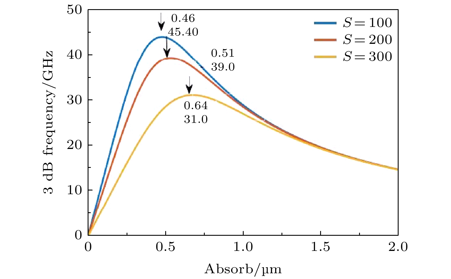
图 1 数值计算的不同吸收区厚度和面积对探测器带宽的影响
Fig. 1. Influence of different thickness and area of absorption region on detector bandwidth is obtained by numerical calculation.
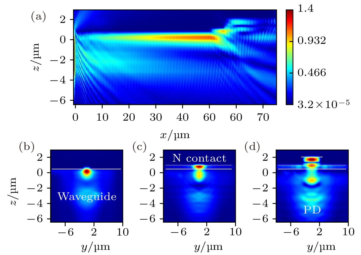
图 3 (a) 倏逝波耦合波导型探测器光场纵向传输强度分布; (b) 光场传输到脊波导时横向电场截面图; (c) 光场传输到光学匹配层时的横向电场截面; (d) 光场被探测器吸收区吸收时的横向电场截面图
Fig. 3. (a) Longitudinal propagation intensity distribution of evanescent coupled waveguide detector; (b) cross section of transverse electric field when light field propagates to ridge waveguide; (c) cross section of transverse electric field in optical matching layer; (d) cross section of transverse electric field when light field is absorbed by absorption region of detector.
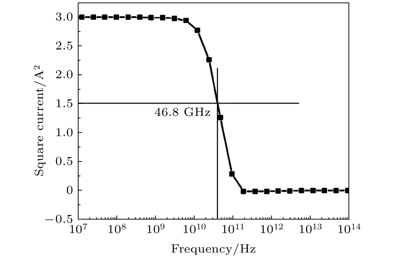
图 4 –5 V偏压, 1 mW/cm2小信号下器件的高频响应
Fig. 4. High frequency response of the device under –5 V bias and 1 mW/cm2 small signal.
表 1 倏逝波导耦合PIN探测器外延结构
Table 1. Epitaxial structure of evanescent waveguide coupled PIN detector.
Function Component $ {\lambda }_{\mathrm{g}} $ Doping Thickness/nm P contact P-In0.53Ga0.47As 1.69 Zn: 1019 80 Grading 1 P-In0.3Ga0.64AsP 1.32 Zn: 5×10¹⁸ 5 Cladding P-In0.18Ga0.39AsP 1.14 Zn: 1018 410 Spacer P-In0.18Ga0.39AsP 1.14 Zn: 5×10¹⁷ 30 Grading 2 P-In0.34Ga0.73AsP 1.396 Zn: 1017 5 Absoption In0.53Ga0.47As 1.69 460 Ethc stop 1 InP 10 n-contact N-In0.3Ga0.64AsP 1.32 Si: 2×10¹⁸ 320 Ethc stop 2 InP 10 Diluted waveguide Substrate InP 500000  下载: 导出CSV
-
[1] Poon W A, Luo X, Xu F, Chen H 2009 IEEE J. Proc. 97 1216
Google Scholar
[2] Lira H L R, Manipatruni S, Lipson M 2009 IEEE J. Opt. Express 17 22271
Google Scholar
[3] Xu Q, Schmidt B, Shakya J, Lipson M 2006 Opt. Express 14 9431
Google Scholar
[4] Bosco G, Curri V, Carena A, Poggiolini P, Forghieri F 2011 J. Lightwave Technol. 29 53
Google Scholar
[5] 喻松, 张华, 申静, 张永军, 顾畹仪 2008 物理学报 57 909
Google Scholar
Yu S, Zhang H, Shen J, Zhang Y J, Gu W Y 2008 Acta Phys. Sin. 57 909
Google Scholar
[6] 万峰, 武保剑, 曹亚敏, 王瑜浩, 文峰, 邱昆 2019 物理学报 68 114207
Google Scholar
Wang F, Wu B J, Cao Y M, Wang Y H, Wen F, Qiu K 2019 Acta Phys. Sin. 68 114207
Google Scholar
[7] Heck M J R, Bauters J F, Davenport, M L, Doylend J K 2013 IEEE J. Sel. Top. Quantum Electron. 19 6100117
Google Scholar
[8] Huang B, Xu Z, Wei W, Zan D, Ning G, Zhang Z, Chen H 2011 Opt. Commun. 284 3924
Google Scholar
[9] Kwack M J, Tanemura T, Higo A, Nakano Y 2012 Opt. Express 20 28734
Google Scholar
[10] Zhang X L, Liu S T, Lu D, Zhang R K, Ji C 2015 Chin. Phys. Lett. 32 054202
[11] Nagarajan R, Joyner C H, Schneider R P 2005 IEEE J. Sel. Top. Quantum Electron. 11 50
Google Scholar
[12] ShengZ, Liu L, Joost B, He S L, Dries V T 2010 Opt. Express 18 1756
Google Scholar
[13] Kato K, Hata S, Kozen A, Yoshida J I, Kawano K 1991 J. IEEE Photonics Technol. Lett. 3 473
Google Scholar
[14] Ohnaka K, Inoue U T, Hasegawa H N, Serizawa H 1985 IEEE J. Quantum Electron. 21 1236
Google Scholar
[15] Demiguel S, Li N, Li X W, Zheng X G, Kim J, Champbell J C, Lu H F, Anselm A 2003 IEEE Photonics Technol. Lett. 15 1761
[16] Liu S Q, Yang X H, Liu Y, Li B, Han Q 2013 Chin. Phys. B 22 108503
Google Scholar
[17] Giraudet L, Banfi F, Demiguel S, Herve-Gruyer G 1999 IEEE Photonics Technol. Lett. 11 111
[18] Magnin V, Giraudet L, Harari J, Decobert J, Pagnot P, Boucherez E, Decoster D 2002 J. Lightwave Technol. 20 477
Google Scholar
[19] Yang C D, Lei P H, Pong D J, Wu M Y, Ho C L, Ho W J 2004 IEEE J. Quantum Electron. 40 1607
Google Scholar
[20] Wang Y S, Chang S J, Chiou Y Z, Lin W 2009 J. Electrochem. Soc. 155 307

 下载:
下载:

计量
- 文章访问数: 8365
- PDF下载量: 136
- 被引次数: 0
