


-
近年来, 二维铁电异质结在高密度存储及光电器件等领域展现了应用潜能, 开发新颖二维铁电异质结是当前的一个重要研究方向. 本论文采用第一性原理计算研究二维铁电材料α-In2Se3与二维单层InSe组成的In2Se3/InSe垂直异质结的能带结构及应力调控. 计算表明, In2Se3/InSe异质结为间接带隙半导体, 具有II型能带匹配. 当In2Se3的极化方向垂直表面朝外时, 带隙大小为0.50 eV, 价带顶和导带底分别来自于InSe和In2Se3; 当In2Se3的极化方向指向面内时, 带隙降低0.04 eV, 价带顶和导带底的来源互换. 在面内拉伸下, 拉伸度越大, 带隙越小. 当极化方向指向面外(内)时, 在双轴拉伸应变达到6%(8%)及以上时会使异质结由半导体转变为导体; 在双轴压缩应变为–6%(–8%)下还可使异质结由间接带隙变为直接带隙; 对于单轴拉伸及压缩, 定性结果与双轴应变一致. 本论文的研究结果表明改变极化方向和施加应力是调控二维In2Se3/InSe铁电异质结的有效方式, 可为设计相关铁电器件提供理论参考.In recent years, two-dimensional ferroelectric heterojunctions have shown potential applications in the fields of high-density storage and optoelectronic devices. The development of novel two-dimensional ferroelectric heterojunctions is an important current research direction. In this work, first-principles calculations are used to study the band structure and stress control of In2Se3/InSe vertical heterojunction composed of two-dimensional ferroelectric material α-In2Se3 and monolayer InSe. The calculations show that the In2Se3/InSe heterojunction is an indirect band gap semiconductor with type-II band matching. When the polarization direction of In2Se3 is perpendicular to the surface facing outward, the band gap is 0.50 eV, and the top and bottom of the valence band originate from InSe and In2Se3 respectively; when the polarization direction of In2Se3 points inward the plane, the band gap decreases by 0.04 eV, and the sources of the top of the valence band and the bottom of the conduction band are interchanged. Under in-plane stretching, the greater the degree of stretching, the smaller the band gap is. After a certain threshold is exceeded, the heterojunction changes from a semiconductor into a conductor, which can also change the heterojunction with an indirect band gap into that with a direct band gap. The research results of this work show that changing the polarization direction and applying stress is an effective way to control the two-dimensional In2Se3/InSe ferroelectric heterojunction, which can provide a theoretical reference for designing the relevant ferroelectric devices.
-
Keywords:
- two-dimensional ferroelectric heterojunction /
- band modulation /
- mechanical strain /
- first principles
[1] Novoselov K S, Geim A K, Morozov S V, Jiang D, Zhang Y, Dubonos S V, Grigorieva I V, Firsov A A 2004 Science 306 666
 Google Scholar
[2] Lu W, Nan H, Hong J, Chen Y, Zhu C, Liang Z, Ma X, Ni Z, Jin C, Zhang Z 2014 Nano Res. 7 853
Google Scholar
[3] Lalmi B, Oughaddou H, Enriquez H, Kara A, Vizzini S, Ealet B, Aufray B 2010 Appl. Phys. Lett. 97 183
[4] Guo J, Chen X, Jin S, Zhang M, Liang C 2015 Catal. Today 246 165
Google Scholar
[5] Haigh S J, Gholinia A, Jalil R, Romani S, Britnell L, Elias D C, Novoselov K S, Ponomarenko L A, Geim A K, Gorbachev R 2012 Nat. Mater. 11 764
Google Scholar
[6] Bertolazzi S, Krasnozhon D, Kis A 2013 ACS Nano 7 3246
Google Scholar
[7] Tongay S, Fan W, Kang J, Park J, Koldemir U, Suh J, Narang D S, Liu K, Ji J, Li J, Sinclair R, Wu J 2014 Nano Lett. 14 3185
Google Scholar
[8] Shim G W, Yoo K, Seo S B, Shin J, Jung D Y, Kang I S, Ahn C W, Cho B J, Choi S Y 2014 Acs Nano 8 6655
Google Scholar
[9] Zhao Z, Xu K, Ryu H, Zhu W 2020 ACS Appl. Mater. Interf. 12 51820
Google Scholar
[10] Ayadi T, Debbichi L, Badawi M, Said M, Kim H, Rocca D, Lebègue S 2019 Physica E: Low-dimens. Syst. Nanostruct. 114 113582
Google Scholar
[11] Li Y, Chen C, Li W, Mao X, Liu H, Xiang J, Nie A, Liu Z, Zhu W, Zeng H 2020 Adv. Electron. Mater. 6 2000061
Google Scholar
[12] Zheng Z, Yao J, Yang G 2017 ACS Appl. Mater. Interf. 9 7288
Google Scholar
[13] Ayadi T, Debbichi L, Badawi M, Said M, Rocca D, Lebègue S 2021 Appl. Surf. Sci. 538 148066
Google Scholar
[14] Zhou B, Jiang K, Shang L, Zhang J, Li Y, Zhu L, Gong S J, Hu Z, Chu J 2020 J. Mater. Chem. C 8 11160
Google Scholar
[15] Dhakal K P, Roy S, Jang H, Chen X, Yun W S, Kim H, Lee J, Kim J, Ahn J H 2017 Chem. Mater. 29 5124
Google Scholar
[16] Desai S B, Seol G, Kang J S, Fang H, Battaglia C, Kapadia R, Ager J W, Guo J, Javey A 2014 Nano Lett. 14 4592
Google Scholar
[17] Guo Y, Li B, Huang Y, Du S, Sun C, Luo H, Liu B, Zhou X, Yang J, Li J, Gu C 2020 Nano Res. 13 2072
Google Scholar
[18] Liu X, Song C, Wu Z, Wang J, Pan J, Li C 2020 J. Phys. D: Appl. Phys. 53 385002
Google Scholar
[19] Rahimi K 2021 Mater. Lett. 282 128680
Google Scholar
[20] Grimme S, Antony J, Ehrlich S, Krieg H 2010 J. Chem. Phys. 132 154104
Google Scholar
[21] Ding Y M, Shi J J, Xia C, Zhang M, Du J, Huang P, Wu M, Wang H, Cen Y L, Pan S H 2017 Nanoscale 9 14682
Google Scholar
[22] Hu T, Zhou J, Dong J 2017 Phys. Chem. Chem. Phys. 19 21722
Google Scholar
[23] Ding W, Zhu J, Wang Z, Gao Y, Xiao D, Gu Y, Zhang Z, Zhu W 2017 Nat. Commun. 8 14956
Google Scholar
[24] Zhou B, Gong SJ, Jiang K, Xu L, Zhu L, Shang L, Li Y, Hu Z, Chu J 2019 J. Phys.: Condens. Matter. 32 055703
[25] Bultinck P 2007 Faraday Discuss. 135 347
Google Scholar
[26] Catalan G, Lubk A, Vlooswijk A H G, et al. 2011 Nat. Mater. 10 963
Google Scholar
[27] Cao Y, Chen L Q, Kalinin S V 2017 Appl. Phys. Lett. 110 202903
Google Scholar
-
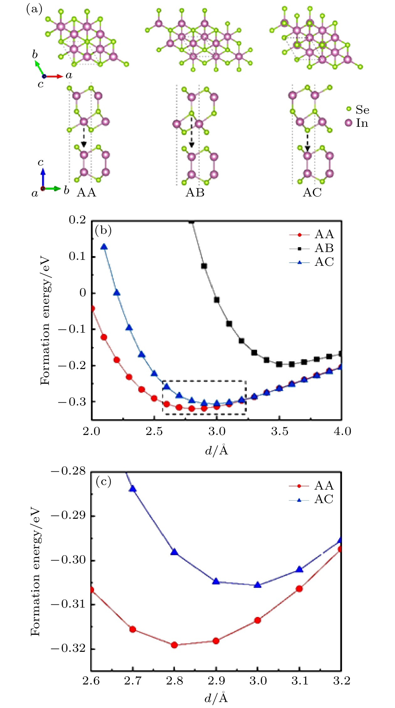
图 1 (a) InSe/In2Se3异质结的3种堆叠方式, 黑色虚线箭头标注了异质结不同层的In原子的位置关系; (b) 3种结构在不同层间距下的能量; (c)图1(b)中黑色虚框部分的局部放大图
Fig. 1. (a) Three stacking methods of InSe/In2Se3heterojunctions, where black dashed arrows mark the positional relationship of In atoms in different layers of the heterojunction; (b) formation energy of the three structures at different layer spacings; (c) a partial enlarged view of the black dashed part in Fig.1 b).
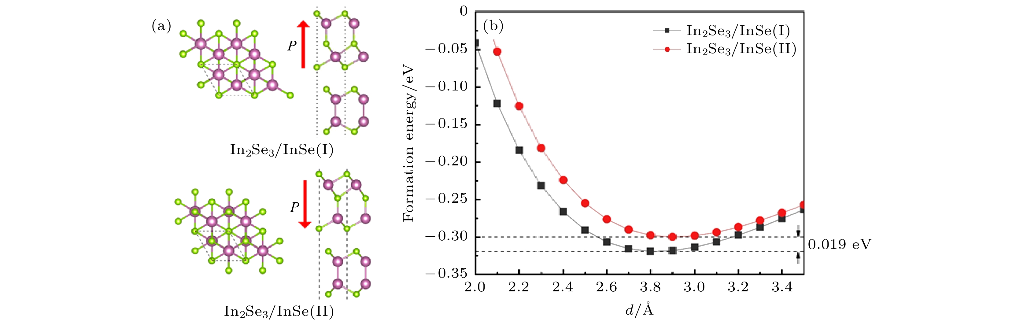
图 2 (a) In2Se3/InSe (I)和In2Se3/InSe (II)的晶格结构, 黑色虚框表示晶格, 红色箭头表示异质结中In2Se3的自发极化方向; (b) In2Se3/InSe (I)和In2Se3/InSe (II)的结合能对比
Fig. 2. (a) Lattice structure of In2Se3/InSe (I) and In2Se3/InSe (II), where the black dashed frame represents the crystal lattice, and the red arrow represents the spontaneous polarization direction of In2Se3; (b) binding energy comparison of In2Se3/InSe (I) and In2Se3/InSe (II).
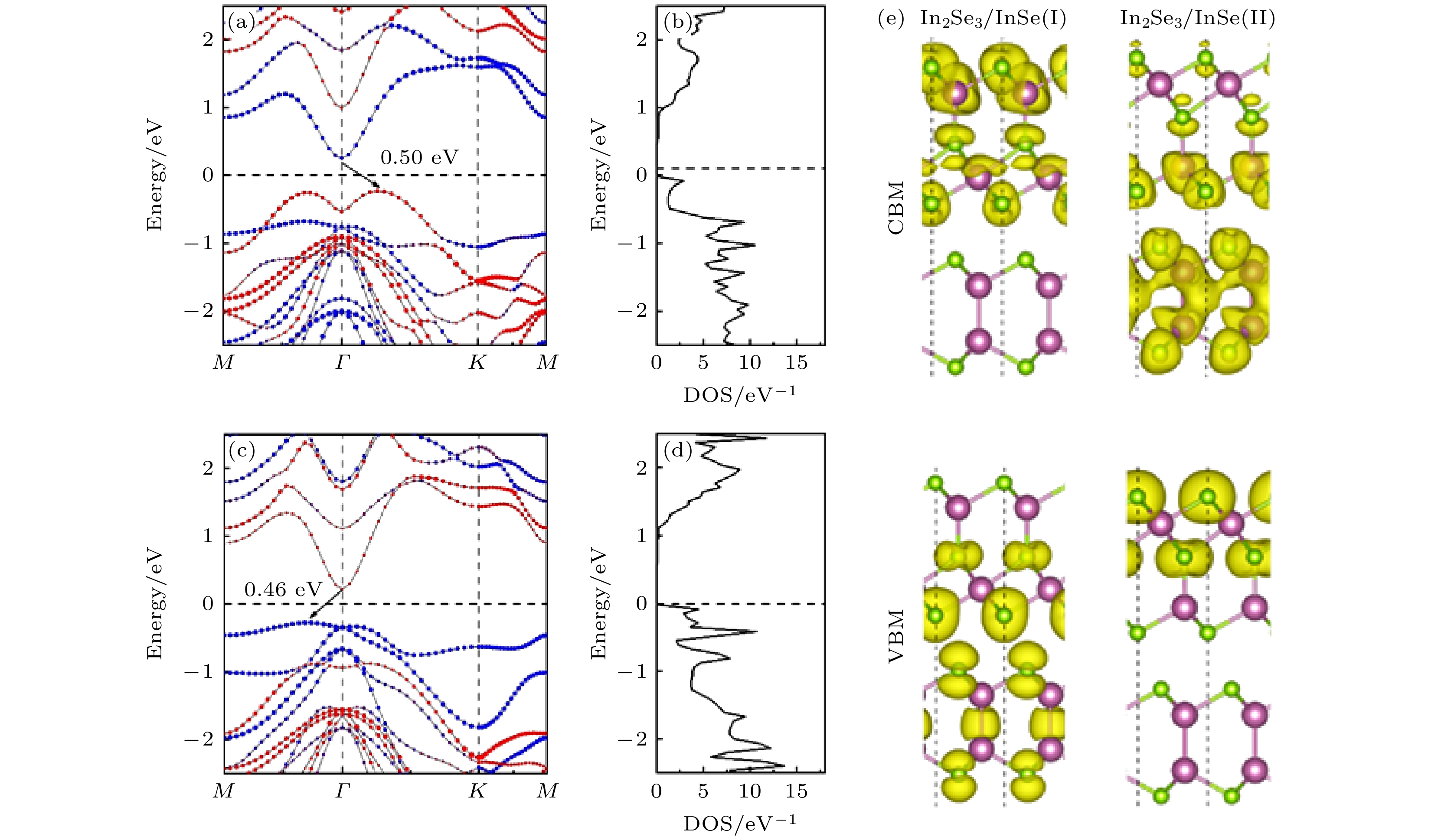
图 3 (a) In2Se3/InSe (I)的能带结构及(b)态密度; (c) In2Se3/InSe (II)的能带结构及(d)态密度. 能带图中红色和蓝色表示InSe及In2Se3对能带的贡献, 黑色箭头表示带隙, 由CBM指向VBM;(e)In2Se3/InSe (I)和In2Se3/InSe (II) CBM和VBM所在能带的电荷空间分布
Fig. 3. (a) Band structure of In2Se3/InSe (I) and (b) density of states; (c) band structure of In2Se3/InSe (II) and (d) density of states, where the red and blue in the energy band diagram indicate the contribution of InSe and In2Se3 to the energy band, and the black arrow indicates the band gap, pointing from CBM to VBM; (e) decomposed charge densities of CBM and VBM for In2Se3/InSe (I) and In2Se3/InSe (II).

图 4 (a) In2Se3/InSe (I) 和 (b) In2Se3/InSe (II)沿Z方向的平面平均差分电荷密度. 图中黄色和青色包络面分别表示电子的聚集和耗尽区
Fig. 4. (a) Plane-averaged charge density difference forIn2Se3/InSe (I) and (b) In2Se3/InSe (II) at equilibrium distance along the Z direction, where the yellow and cyan envelope areas representelectron accumulation and depletion, respectively.

图 5 双轴应变(左)和单轴应变(右)的晶胞选取以及应变施加方向.
Fig. 5. Unit cell selection and strain application direction of biaxial strain (left) and uniaxial strain (right).

图 6 (a) 不同双轴应变下In2Se3/InSe (I)的带隙; (b)不同双轴应变下In2Se3/InSe (II)的带隙
Fig. 6. (a) Band gap of In2Se3/InSe (I) under biaxial strain; (b) band gap of In2Se3/InSe (II) under biaxial strain.
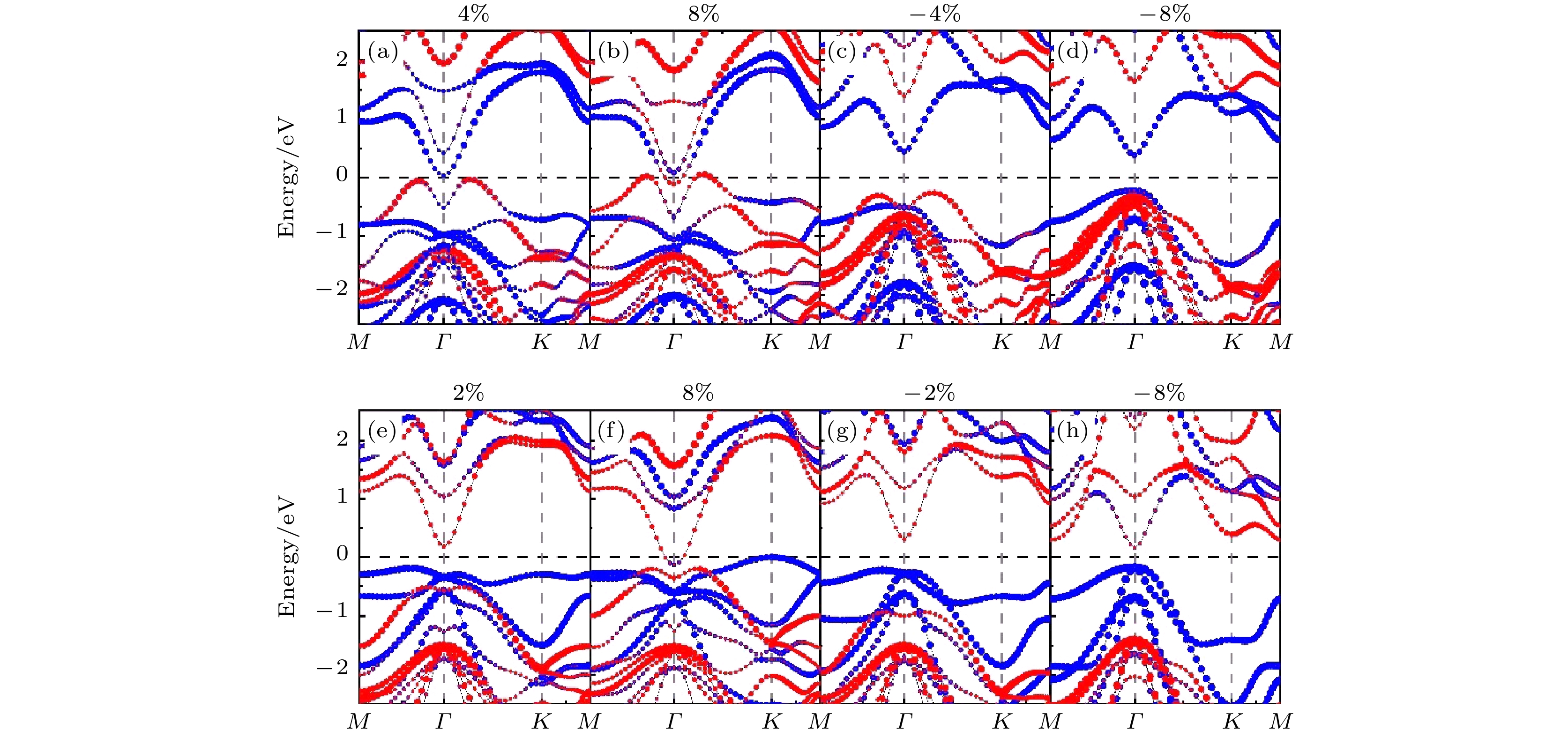
图 7 (a)−(d)4%、8%、–4%和–8%双轴应变下In2Se3/InSe (I)的投影能带结构; (e)−(h) 2%、8%、–2%和–8%双轴应变下In2Se3/InSe (II)的投影能带结构. 能带图中红色部分表示InSe对能带的贡献, 蓝色部分表示In2Se3对能带的贡献
Fig. 7. (a)−(d) The projected band structure of In2Se3/InSe (I) under 4%, 8%, –4% and –8% biaxial strain; (e)−(h) Projected band structure of In2Se3/InSe (II) under 2%, 8%, –2% and –8% biaxial strain. The red part of the energy band indicates the contribution of InSe, the blue part indicates the contribution of In2Se3.
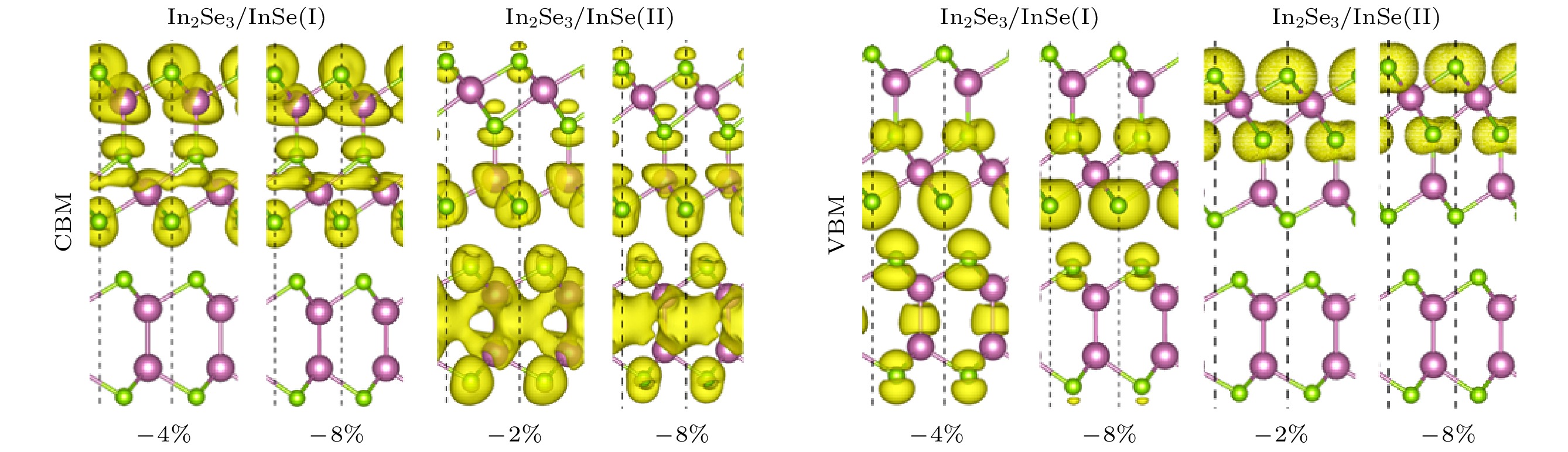
图 8 –4%和–8%双轴应变下In2Se3/InSe(I)CBM和VBM所在能带的电荷空间分布以及–2%及–8%双轴应变下In2Se3/InSe (II)CBM和VBM所在能带的电荷空间分布
Fig. 8. Decomposed charge densities of CBM and VBM for In2Se3/InSe (I) under –4% and –8% biaxial strain and thedecomposed charge densities of CBM and VBM for In2Se3/InSe (II) under –2% and –8% biaxial strain.
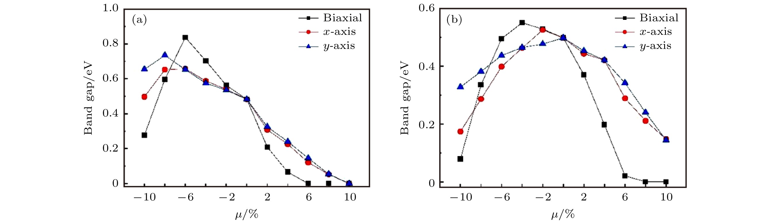
图 9 (a) x方向与y方向单轴应变和双轴应变下In2Se3/InSe (I)的带隙; (b) x方向与y方向单轴应变和双轴应变下In2Se3/InSe (II)的带隙
Fig. 9. (a) Band gap of In2Se3/InSe (I) under x-axis strain, y-axis strain and biaxial strain; (b) band gap of In2Se3/InSe (II) under x-axis strain, y-axis strain and biaxial strain.
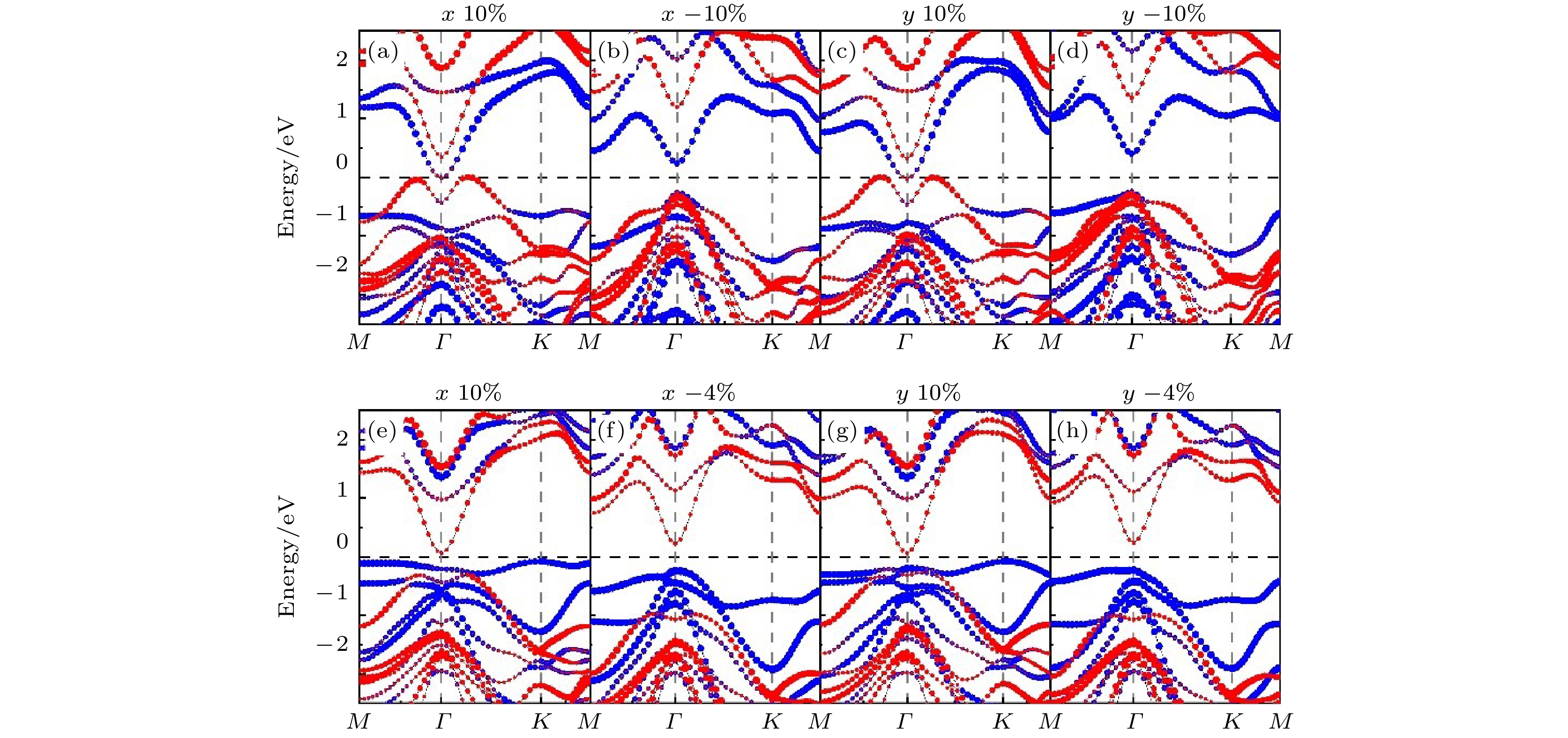
图 10 (a)−(d)x和y方向10%、–10%应变下In2Se3/InSe (I)的投影能带结构; (e)−(h)x和y方向10%、–4%应变下In2Se3/InSe (II)的投影能带结构. 能带图中红色部分表示InSe对能带的贡献, 蓝色部分表示In2Se3对能带的贡献
Fig. 10. (a)−(d) Projected band structure of In2Se3/InSe (I) under 10%, –10% x-axis strain and 10%, –10% y-axis strain; (e)−(h) projected band structure of In2Se3/InSe (II) under 10%, –4% x-axis strain and 10%, –4% y-axis strain. The red part of the energy band indicates the contribution of InSe, the blue part indicates the contribution of In2Se3.
表 1 双轴应变下In2Se3/InSe (II)及In2Se3/InSe (I)的带隙.
Table 1. Band gap of In2Se3/InSe (I) and In2Se3/ InSe(II) under biaxial strain.
μ/% In2Se3/InSe (I) In2Se3/InSe (II) Gap/eV Character Gap/eV Character –10 0.28 direct 0.08 direct –8 0.60 direct 0.34 direct –6 0.84 direct 0.50 indirect –4 0.70 indirect 0.55 indirect –2 0.56 indirect 0.53 indirect 0 0.50 indirect 0.46 indirect 2 0.21 indirect 0.37 indirect 4 0.07 indirect 0.20 indirect 6 — metallic 0.02 indirect 8 — metallic — metallic 10 — metallic — metallic  下载: 导出CSV
-
[1] Novoselov K S, Geim A K, Morozov S V, Jiang D, Zhang Y, Dubonos S V, Grigorieva I V, Firsov A A 2004 Science 306 666
Google Scholar
[2] Lu W, Nan H, Hong J, Chen Y, Zhu C, Liang Z, Ma X, Ni Z, Jin C, Zhang Z 2014 Nano Res. 7 853
Google Scholar
[3] Lalmi B, Oughaddou H, Enriquez H, Kara A, Vizzini S, Ealet B, Aufray B 2010 Appl. Phys. Lett. 97 183
[4] Guo J, Chen X, Jin S, Zhang M, Liang C 2015 Catal. Today 246 165
Google Scholar
[5] Haigh S J, Gholinia A, Jalil R, Romani S, Britnell L, Elias D C, Novoselov K S, Ponomarenko L A, Geim A K, Gorbachev R 2012 Nat. Mater. 11 764
Google Scholar
[6] Bertolazzi S, Krasnozhon D, Kis A 2013 ACS Nano 7 3246
Google Scholar
[7] Tongay S, Fan W, Kang J, Park J, Koldemir U, Suh J, Narang D S, Liu K, Ji J, Li J, Sinclair R, Wu J 2014 Nano Lett. 14 3185
Google Scholar
[8] Shim G W, Yoo K, Seo S B, Shin J, Jung D Y, Kang I S, Ahn C W, Cho B J, Choi S Y 2014 Acs Nano 8 6655
Google Scholar
[9] Zhao Z, Xu K, Ryu H, Zhu W 2020 ACS Appl. Mater. Interf. 12 51820
Google Scholar
[10] Ayadi T, Debbichi L, Badawi M, Said M, Kim H, Rocca D, Lebègue S 2019 Physica E: Low-dimens. Syst. Nanostruct. 114 113582
Google Scholar
[11] Li Y, Chen C, Li W, Mao X, Liu H, Xiang J, Nie A, Liu Z, Zhu W, Zeng H 2020 Adv. Electron. Mater. 6 2000061
Google Scholar
[12] Zheng Z, Yao J, Yang G 2017 ACS Appl. Mater. Interf. 9 7288
Google Scholar
[13] Ayadi T, Debbichi L, Badawi M, Said M, Rocca D, Lebègue S 2021 Appl. Surf. Sci. 538 148066
Google Scholar
[14] Zhou B, Jiang K, Shang L, Zhang J, Li Y, Zhu L, Gong S J, Hu Z, Chu J 2020 J. Mater. Chem. C 8 11160
Google Scholar
[15] Dhakal K P, Roy S, Jang H, Chen X, Yun W S, Kim H, Lee J, Kim J, Ahn J H 2017 Chem. Mater. 29 5124
Google Scholar
[16] Desai S B, Seol G, Kang J S, Fang H, Battaglia C, Kapadia R, Ager J W, Guo J, Javey A 2014 Nano Lett. 14 4592
Google Scholar
[17] Guo Y, Li B, Huang Y, Du S, Sun C, Luo H, Liu B, Zhou X, Yang J, Li J, Gu C 2020 Nano Res. 13 2072
Google Scholar
[18] Liu X, Song C, Wu Z, Wang J, Pan J, Li C 2020 J. Phys. D: Appl. Phys. 53 385002
Google Scholar
[19] Rahimi K 2021 Mater. Lett. 282 128680
Google Scholar
[20] Grimme S, Antony J, Ehrlich S, Krieg H 2010 J. Chem. Phys. 132 154104
Google Scholar
[21] Ding Y M, Shi J J, Xia C, Zhang M, Du J, Huang P, Wu M, Wang H, Cen Y L, Pan S H 2017 Nanoscale 9 14682
Google Scholar
[22] Hu T, Zhou J, Dong J 2017 Phys. Chem. Chem. Phys. 19 21722
Google Scholar
[23] Ding W, Zhu J, Wang Z, Gao Y, Xiao D, Gu Y, Zhang Z, Zhu W 2017 Nat. Commun. 8 14956
Google Scholar
[24] Zhou B, Gong SJ, Jiang K, Xu L, Zhu L, Shang L, Li Y, Hu Z, Chu J 2019 J. Phys.: Condens. Matter. 32 055703
[25] Bultinck P 2007 Faraday Discuss. 135 347
Google Scholar
[26] Catalan G, Lubk A, Vlooswijk A H G, et al. 2011 Nat. Mater. 10 963
Google Scholar
[27] Cao Y, Chen L Q, Kalinin S V 2017 Appl. Phys. Lett. 110 202903
Google Scholar

 下载:
下载:
计量
- 文章访问数: 15959
- PDF下载量: 805
- 被引次数: 0
