


-
超导涡旋运动引起的棘齿效应可以广泛应用于磁通泵、整流器和超导开关等装置. 金兹堡-朗道理论是研究超导磁通涡旋问题强有力的工具和手段. 本文采用有限差分法数值求解时间相关的金兹堡-朗道方程, 利用快速傅里叶变换方法求解耦合的热传导方程, 数值模拟了临界温度梯度超导薄膜磁通涡旋动力学行为, 提出了一种新的调节超导整流效应的方式, 并研究了临界温度梯度大小和缺陷位置对超导整流电压反转现象的影响规律. 由于超导边界势垒和缺陷吸引势对磁通涡旋的共同作用, 当缺陷位置偏向临界温度较高的一侧或者临界温度梯度较小时有利于观察到整流电压随交流幅值增大发生的反转现象.The ratchet effect caused by superconducting vortex motion can be widely used in flux pumps, rectifiers and superconducting switches. Ginzburg-Landau theory provides a powerful tool to investigate superconducting vortex matter. In this paper, the finite difference method is used to numerically solve the time-dependent Ginzburg-Landau equation, and the fast Fourier transform method is used to solve the coupled heat conduction equation. The vortex dynamic behavior of the superconducting thin film with a linear change of critical temperature is simulated numerically, and a new way to regulate the superconducting rectification effect is proposed. The effect of critical temperature gradient and slit location on the reversal phenomenon of rectified voltage are studied. Because of the influence of edge barrier and the defect attraction potential on vortex motion, it is beneficial to observing the reversal rectified voltage with increasing AC amplitude that the defect location is near to the side of the higher critical temperature or the gradient of the critical temperature is small.
-
Keywords:
- superconducting film /
- rectified voltage /
- critical temperature gradient /
- slit
[1] Silhanek A V, van Look L, Raedts S, Jonckheere R, Moshchalkov V V 2003 Phys. Rev. B 68 214504
 Google Scholar
[2] Silhanek A V, Gillijns W, Moshchalkov V V, Metlushko V, Ilic B 2006 Appl. Phys. Lett. 89 182505
Google Scholar
[3] Milošević M V, Gillijns W, Silhanek A V, Libál A, Peeters F M, Moshchalkov V V 2010 Appl. Phys. Lett. 96 032503
Google Scholar
[4] Hänggi P, Marchesoni F 2009 Rev. Mod. Phys. 81 387
Google Scholar
[5] Ooi S, Savel’ev S, Gaifullin M B, Mochiku T, Hirata K, Nori F 2007 Phys. Rev. Lett. 99 207003
Google Scholar
[6] Marrocco N, Pepe G P, Capretti A, Parlato L, Pagliarulo V, Peluso G, Barone A, Cristiano R, Ejrnaes M, Casaburi A, Kashiwazaki N, Taino T, Myoren H, Sobolewski R 2010 Appl. Phys. Lett. 97 092504
Google Scholar
[7] Kremen A, Wissberg S, Haham N, Persky E, Frenkel Y, Kalisky B 2016 Nano Lett. 16 1626
Google Scholar
[8] Semenov A, Charaev I, Lusche R, Ilin K, Siegel M, Hübers H W, Bralović N, Dopf K, Vodolazov D Y 2015 Phys. Rev. B 92 174518
Google Scholar
[9] Berdiyorov G R, MiloševićM V, Peeters F M 2012 Appl. Phys. Lett. 100 262603
Google Scholar
[10] Lee C S, Jankó B, Derényi I, Barabá si A L 1999 Nature 400 337
Google Scholar
[11] Zhu B Y, Marchesoni F, Nori F 2004 Phys. Rev. Lett. 92 180602
Google Scholar
[12] Olson C J, Reichhardt C, Janko B, Nori F 2001 Phys. Rev. Lett. 87 177002
Google Scholar
[13] van de Vondel J, Gladilin V N, Silhanek A V, Gillijns W, Tempere J, Devreese J T, Moshchalkov V V 2011 Phys. Rev. Lett. 106 137003
Google Scholar
[14] Lu Q M, Olson Reichhardt C J, Reichhardt C 2007 Phys. Rev. B 75 054502
Google Scholar
[15] Berdiyorov G R, Milošević M V, Covaci L, Peeters F M 2011 Phys. Rev. Lett. 107 177008
Google Scholar
[16] He A, Xue C, Zhou Y H 2018 Chin. Phys. B 27 057402
Google Scholar
[17] Ooi S, Mochikua T, Hirataa K 2008 Physica C 468 1291
Google Scholar
[18] Wu T C, Horng L, Wu J C, Cao R, Koláček J, Yang T J 2007 J. Appl. Phys. 102 033918
Google Scholar
[19] Reichhardt C, Ray D, Olson Reichhardt C J 2015 Phys. Rev. B 91 184502
Google Scholar
[20] Gillijns W, Silhanek A V, Moshchalkov V V, Olson Reichhardt C J, Reichhardt C 2007 Phys. Rev. Lett. 99 247002
Google Scholar
[21] Adami O A, Cerbu D, Cabosart D, Motta M, Cuppens J, Ortiz W A, Moshchalkov V V, Hackens B, Delamare R, Van de Vondel J, Silhanek A V 2013 Appl. Phys. Lett. 102 052603
Google Scholar
[22] Ji J D, Yuan J, He G, Jin B H, Zhu B Y, Kong X D, Jia X Q, Kang L, Jin K, Wu P H 2016 Appl. Phys. Lett. 109 242601
Google Scholar
[23] Wang Y L, Ma X Y, Xu J, Xiao Z L, Snezhko A, Divan R, Ocola L E, Pearson J E, Janko B Wai K K 2018 Nat. Nanotechnol. 13 560
Google Scholar
[24] Villegas J E, Savel’ev S, Nori F, Gonzalez E M, Anguita J V, Garcia R, Vicent J L 2003 Science 302 1188
Google Scholar
[25] de Souza Silva C C, van de Vondel J, Morelle M, Moshchalkov V V 2006 Nature 440 651
Google Scholar
[26] de Souza Silva C C, Silhanek A V, van de Vondel J, Gillijns W, Metlushko V, Ilic B, Moshchalkov V V 2007 Phys. Rev. Lett. 98 117005
Google Scholar
[27] He A, Xue C, Zhou Y H 2019 Appl. Phys. Lett. 115 032602
Google Scholar
[28] He A, Xue C 2020 Chin. Phys. B 29 127401
Google Scholar
[29] Kramer L, Watts-Tobin R J 1978 Phys. Rev. Lett. 40 1041
Google Scholar
[30] Berdiyorov G, Harrabi K, Oktasendra F, Gasmi K, Mansour A I, Maneval J P, Peeters F M 2014 Phys. Rev. B 90 054506
Google Scholar
[31] Sadovskyya I A, Kosheleva A E, Phillipsb C L, Karpeyevc D A, Glatz A 2015 J. Comput. Phys. 294 639
Google Scholar
[32] Berdiyorov G R, MiloševićM V, Latimer M L, Xiao Z L, Kwok W K, Peeters F M 2012 Phys. Rev. Lett. 109 057004
Google Scholar
[33] Vodolazov D Y, Peeters F M, Morelle M, Moshchalkov V V 2005 Phys. Rev. B 71 184502
Google Scholar
[34] Adami O A, Jelić Ž L, Xue C, Abdel-Hafiez M, Hackens B, Moshchalkov V V, Milošević M V, Van de Vondel J, Silhanek A V 2015 Phys. Rev. B 92 134506
Google Scholar
[35] Sadovskyy I A, Koshelev A E, Glatz A, Ortalan V, Rupich M W, Leroux M 2016 Phys. Rev. Appl. 5 014011
Google Scholar
-

图 1 含长方形缺陷的临界温度梯度超导薄膜示意图, 临界温度沿着y轴从
$T_{{\rm{cmin}}}$ 线性增大到$T_{{\rm{cmax}}}$ . 超导薄膜宽为w, 沿着x轴无限长, 缺陷的长度和宽度分别为$c_{\rm{l}}$ 和$c_{\rm{w}}$ , 缺陷中心距离临界温度较低$T_{{\rm{cmin}}}$ 的下边界为$C_{\rm{p}}$ . 沿着x轴的一方形波交流电$I_{{\rm{a}}}(t)$ 和沿着z轴的垂直磁场加载于超导薄膜, 沿着电流加载方向计算直流电压$V_{{\rm{dc}}}$ , 磁通涡旋沿着y轴方向运动.Fig. 1. Schematic diagram of critical temperature gradient superconducting film with slit. The critical temperature increases linearly from
$T_{{\rm{cmin}}}$ upward to$T_{{\rm{cmax}}}$ along the y axis. The superconducting film of width w is infinite along x axis. The slit length and width are$c_{\rm{l}}$ and$c_{\rm{w }}$ , respectively. The distance of defect center to sample upper boundary is$C_{\rm{P}}$ . Superconducting film is applied by a square-wave ac current$I_{{\rm{a}}}(t)$ along x axis and a perpendicular magnetic field$H_{\rm{a}}$ along z axis, and the DC voltage$V_{{\rm{dc}}}$ is calculated along the direction of applied current. The direction of vortex motion is along y axis.
图 2 (a)不同磁场和正反电流下电流-电压(I-V)特征曲线, 插图1—插图6表示I-V曲线上对应点的超导电子密度. 红色箭头表示输运电流的加载方向, 黑色箭头代表涡旋的运动方向. (b)缺陷位于样品中心
$ C_{\rm{p}} = w/2 $ 时整流电压随交流幅值的变化规律. 超导样品上下边界的临界温度分别为$T_{{\rm{cmax}}} = 12\; {\rm{K }}$ 和$T_{{\rm{cmin}}} = 4.7 \;{\rm{K}}$ (见多媒体动画A1 )Fig. 2. (a) Characteristic curves of current-voltage (I-V) at several magnetic fields for
$ +I_{\rm{a}} $ and$ -I_{\rm{a}} $ . Snapshots 1–6 indicate the corresponding cooper-pair density shown in the I-V curves; (b) variations of rectified voltage as a function of ac amplitude for slit located at the middle of the sample$ C_{\rm{p}} = w/2 $ . The critical temperature of superconducting film at the top and bottom boundary are$T_{{\rm{cmax}}} = 12\;{\rm{ K}}$ and$T_{{\rm{cmin}}} = 4.7\; {\rm{K}}$ , respectively (multimedia viewA1 of the supplementary materials).
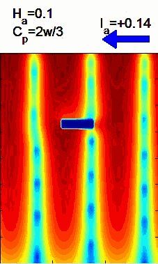
图 3 不同磁场下(a)缺陷靠近样品下边界
$ C_{\rm{p}} = w/3 $ 和(b)缺陷靠近样品上边界$ C_{\rm{p }}= 2 w/3 $ 时整流电压随交流幅值的变化规律. 超导样品上下边界的临界温度分别为$T_{{\rm{cmax}}} = 12 \;{\rm{K}}$ 和$T_{{\rm{cmin}}} = 4.7\; {\rm{K}}$ (见补充材料动画A2 和A3 )Fig. 3. Variations of rectified voltage as a function of ac amplitude for several magnetic fields with defect located at (a)
$ C_{\rm{p}} = w/3 $ and (b)$ C_{\rm{p}} = 2 w/3 $ . The critical temperature of superconducting film at the top and bottom boundary are$T_{{\rm{cmax}}} {=} 12\; {\rm{K}}$ and$T_{{\rm{cmin}}} {=} 4.7\; {\rm{K}}$ , respectively (multimedia viewA2 andA3 of the supplementary materials).
图 4 缺陷靠近样品上边界(
$ C_{\rm{p}} = 2 w/3 $ )和磁场$ H_{{\rm{a}}} = 0.1 $ 时超导处于平衡状态下, 当电流幅值(a)$I_{{\rm{ac}}} = 0.13$ 和(b)$I_{{\rm{ac}}} = $ $ 0.14$ 时电压随时间的周期振荡曲线. 插图表示V-t曲线上对应点的超导电子密度云图, 黑色箭头代表涡旋的运动方向. 超导样品上下边界的临界温度分别为$T_{{\rm{cmax}}} = 12\;{\rm{ K}}$ 和$T_{{\rm{cmin}}} = 4.7\; {\rm{K}}$ Fig. 4. Variations of equilibrated voltage as a function of ac amplitude time with magnetic field
$ H_{{\rm{a}}} = 0.1 $ and slit location$ C_{\rm{p}} = 2 w/3 $ for (a)$ I_{{\rm{ac}}} = 0.13 $ and (b)$ I_{{\rm{ac}}} = 0.14 $ . Snapshots indicate the corresponding Cooper-pair density shown in the V-t curves. The black arrows indicate the direction of vortex motion. The critical temperature of superconducting film at the top and bottom boundary are$T_{{\rm{cmax}}} = 12 \;{\rm{K}}$ and$T_{{\rm{cmin}}} = 4.7\; {\rm{K}}$ , respectively.
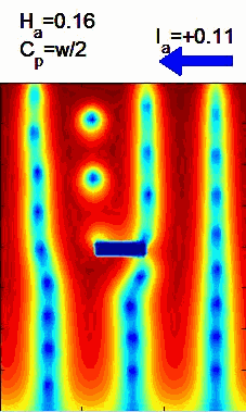
图 5 缺陷位置为(a)
$ C_{\rm{p}} = w/2 $ 和(b)$ C_{\rm{p}} = 2 w/3 $ 时整流电压随磁场和电流变化的相图. 白色虚线代表整流电压发生反转的区域. 插图表示缺陷位置$ C_{\rm{p}} = 2 w/3 $ 时不同磁场下和电流下的超导电子密度, 左栏表示正方向加载电流的情形, 右栏表示负方向加载电流的情形, 黑色箭头表示涡旋的运动方向. 超导样品上下边界的临界温度分别为$T_{{\rm{cmax}}} = 12\; {\rm{K}}$ 和$T_{{\rm{cmin}}} = 4.7\;{\rm{ K}}$ Fig. 5. Contour plot of
$ V_{{\rm{dc}}} $ as a function of magnetic field and current amplitude with slit location (a)$ C_{\rm{p}} = w/2 $ and (b)$ C_{\rm{p}} = $ $ 2 w/3 $ . The white dotted lines represent the area of reversal rectified voltage. Snapshots show the superconducting Cooper-pair density at the defect location$ C_{\rm{p}} = 2 w/3 $ under different magnetic fields and currents. The left column represents the condition of applied current along the positive direction, and the right column represents that of applied current along the negative direction. The black arrows represent the direction of vortex motion. The critical temperature of superconducting film at the top and bottom boundary are$T_{{\rm{cmax}}} = 12 \;{\rm{K}}$ and$T_{{\rm{cmin}}} = 4.7\; {\rm{K}}$ , respectively.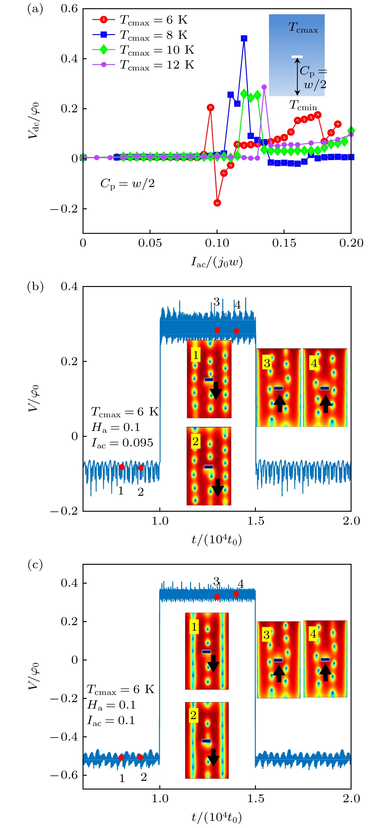
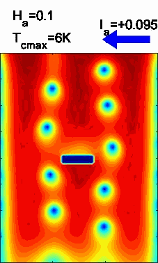
图 6 (a)缺陷处于样品中心(
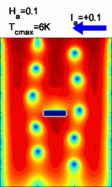
$ C_{\rm{p}} = w/2 $ )、最低临界温度$T_{{\rm{cmin}}} = 4.7\; {\rm{K }}$ 和磁场$ H_{{\rm{a}}} = 0.1 $ , 超导样品上边界的最高临界温度分别为$ T_{{\rm{cmax}}} $ = 6, 8, 10和12 K时整流电压随交流幅值的变化规律; (b)$ I_{{\rm{ac}}} = 0.095 $ 和(c)$I_{{\rm{ac}}} = 0.1$ 超导处于平衡状态时电压随时间的周期振荡曲线. 插图表示V-t曲线上对应点的超导电子密度, 黑色箭头代表涡旋的运动方向(见补充材料多媒体动画A4和A5 )Fig. 6. (a) Variations of rectified voltage as a function of ac amplitude with slit location
$ C_{\rm{p}} = w/2 $ ,$T_{{\rm{cmin}}} = 4.7\; {\rm{K}}$ and magnetic field$ H_{{\rm{a}}} = 0.1 $ for several maximum critical temperature$ T_{{\rm{cmax}}} $ = 6, 8, 10 and 12 K. Dependencies of equilibrated voltage versus time for (b)$ I_{{\rm{ac}}} = 0.095 $ and (c)$ I_{{\rm{ac}}} = $ $ 0.1 $ . Snapshots indicate the corresponding cooper-pair density shown in the V-t curves. The black arrows indicate the direction of vortex motion (multimedia viewA4 and A5 of supplementary materials) -
[1] Silhanek A V, van Look L, Raedts S, Jonckheere R, Moshchalkov V V 2003 Phys. Rev. B 68 214504
Google Scholar
[2] Silhanek A V, Gillijns W, Moshchalkov V V, Metlushko V, Ilic B 2006 Appl. Phys. Lett. 89 182505
Google Scholar
[3] Milošević M V, Gillijns W, Silhanek A V, Libál A, Peeters F M, Moshchalkov V V 2010 Appl. Phys. Lett. 96 032503
Google Scholar
[4] Hänggi P, Marchesoni F 2009 Rev. Mod. Phys. 81 387
Google Scholar
[5] Ooi S, Savel’ev S, Gaifullin M B, Mochiku T, Hirata K, Nori F 2007 Phys. Rev. Lett. 99 207003
Google Scholar
[6] Marrocco N, Pepe G P, Capretti A, Parlato L, Pagliarulo V, Peluso G, Barone A, Cristiano R, Ejrnaes M, Casaburi A, Kashiwazaki N, Taino T, Myoren H, Sobolewski R 2010 Appl. Phys. Lett. 97 092504
Google Scholar
[7] Kremen A, Wissberg S, Haham N, Persky E, Frenkel Y, Kalisky B 2016 Nano Lett. 16 1626
Google Scholar
[8] Semenov A, Charaev I, Lusche R, Ilin K, Siegel M, Hübers H W, Bralović N, Dopf K, Vodolazov D Y 2015 Phys. Rev. B 92 174518
Google Scholar
[9] Berdiyorov G R, MiloševićM V, Peeters F M 2012 Appl. Phys. Lett. 100 262603
Google Scholar
[10] Lee C S, Jankó B, Derényi I, Barabá si A L 1999 Nature 400 337
Google Scholar
[11] Zhu B Y, Marchesoni F, Nori F 2004 Phys. Rev. Lett. 92 180602
Google Scholar
[12] Olson C J, Reichhardt C, Janko B, Nori F 2001 Phys. Rev. Lett. 87 177002
Google Scholar
[13] van de Vondel J, Gladilin V N, Silhanek A V, Gillijns W, Tempere J, Devreese J T, Moshchalkov V V 2011 Phys. Rev. Lett. 106 137003
Google Scholar
[14] Lu Q M, Olson Reichhardt C J, Reichhardt C 2007 Phys. Rev. B 75 054502
Google Scholar
[15] Berdiyorov G R, Milošević M V, Covaci L, Peeters F M 2011 Phys. Rev. Lett. 107 177008
Google Scholar
[16] He A, Xue C, Zhou Y H 2018 Chin. Phys. B 27 057402
Google Scholar
[17] Ooi S, Mochikua T, Hirataa K 2008 Physica C 468 1291
Google Scholar
[18] Wu T C, Horng L, Wu J C, Cao R, Koláček J, Yang T J 2007 J. Appl. Phys. 102 033918
Google Scholar
[19] Reichhardt C, Ray D, Olson Reichhardt C J 2015 Phys. Rev. B 91 184502
Google Scholar
[20] Gillijns W, Silhanek A V, Moshchalkov V V, Olson Reichhardt C J, Reichhardt C 2007 Phys. Rev. Lett. 99 247002
Google Scholar
[21] Adami O A, Cerbu D, Cabosart D, Motta M, Cuppens J, Ortiz W A, Moshchalkov V V, Hackens B, Delamare R, Van de Vondel J, Silhanek A V 2013 Appl. Phys. Lett. 102 052603
Google Scholar
[22] Ji J D, Yuan J, He G, Jin B H, Zhu B Y, Kong X D, Jia X Q, Kang L, Jin K, Wu P H 2016 Appl. Phys. Lett. 109 242601
Google Scholar
[23] Wang Y L, Ma X Y, Xu J, Xiao Z L, Snezhko A, Divan R, Ocola L E, Pearson J E, Janko B Wai K K 2018 Nat. Nanotechnol. 13 560
Google Scholar
[24] Villegas J E, Savel’ev S, Nori F, Gonzalez E M, Anguita J V, Garcia R, Vicent J L 2003 Science 302 1188
Google Scholar
[25] de Souza Silva C C, van de Vondel J, Morelle M, Moshchalkov V V 2006 Nature 440 651
Google Scholar
[26] de Souza Silva C C, Silhanek A V, van de Vondel J, Gillijns W, Metlushko V, Ilic B, Moshchalkov V V 2007 Phys. Rev. Lett. 98 117005
Google Scholar
[27] He A, Xue C, Zhou Y H 2019 Appl. Phys. Lett. 115 032602
Google Scholar
[28] He A, Xue C 2020 Chin. Phys. B 29 127401
Google Scholar
[29] Kramer L, Watts-Tobin R J 1978 Phys. Rev. Lett. 40 1041
Google Scholar
[30] Berdiyorov G, Harrabi K, Oktasendra F, Gasmi K, Mansour A I, Maneval J P, Peeters F M 2014 Phys. Rev. B 90 054506
Google Scholar
[31] Sadovskyya I A, Kosheleva A E, Phillipsb C L, Karpeyevc D A, Glatz A 2015 J. Comput. Phys. 294 639
Google Scholar
[32] Berdiyorov G R, MiloševićM V, Latimer M L, Xiao Z L, Kwok W K, Peeters F M 2012 Phys. Rev. Lett. 109 057004
Google Scholar
[33] Vodolazov D Y, Peeters F M, Morelle M, Moshchalkov V V 2005 Phys. Rev. B 71 184502
Google Scholar
[34] Adami O A, Jelić Ž L, Xue C, Abdel-Hafiez M, Hackens B, Moshchalkov V V, Milošević M V, Van de Vondel J, Silhanek A V 2015 Phys. Rev. B 92 134506
Google Scholar
[35] Sadovskyy I A, Koshelev A E, Glatz A, Ortalan V, Rupich M W, Leroux M 2016 Phys. Rev. Appl. 5 014011
Google Scholar


 下载:
下载:


计量
- 文章访问数: 7048
- PDF下载量: 70
- 被引次数: 0
