


-
利用非平衡格林函数方法, 理论研究了多种组合形式的局域交换场对锡烯纳米带自旋输运性质的影响. 研究表明锡烯自旋相关电导、边缘态和体能带都显著地依赖于不同区域交换场的方向和强度. 在[I:
$ \pm Y $ , II:$ +Z $ , III:$ \pm Y $ ]方向交换场的共同作用下, 边缘态受Y方向交换场影响形成带隙, 禁带宽度与交换场强度M 成正比, 在$ -M<E<M $ 能量范围电导值为0. 对上下边缘区域同时施加$ +Z $ 或$ -Z $ 方向的交换场时, 边缘态和体能带都发生较强的自旋劈裂, 自旋向上和向下能带沿相反方向向高能量区域移动, 增大交换场的强度电导自旋极化的范围将从高能量扩展到低能量区域. 当交换场方向为[I:$ \mp Z $ , II:$ \pm Y $ , III:$ \pm Z $ ]时, 低能区自旋相关的电导保持电子空穴对称性, 不同交换场强度条件下, 自旋相关电导都在相同的能量范围$ -\lambda_{{\rm{so}}}<E< $ $ \lambda_{{\rm{so}}} $ 保持电导平台$ G_\sigma=e^2/h $ .Topological insulator is a new quantum state of matter in which spin-orbit coupling gives rise to topologically protected gapless edge or surface states. The nondissipation transport properties of the edge or surface state make the topological device a promising candidate for ultra-low-power consumption electronics. Stanene is a type of two-dimensional topological insulator consisting of Sn atoms arranged similarly to graphene and silicene in a hexagonal structure. In this paper, the effects of various combinations of local exchange fields on the spin transport of stanene nanoribbons are studied theoretically by using the non-equilibrium Green's function method. The results show that the spin-dependent conductance, edge states, and bulk bands of stanene are significantly dependent on the direction and strength of the exchange field in different regions. Under the joint action of the exchange fields in [I:$ \pm Y $ , II:$ +Z $ , III:$ \pm Y $ ] direction, the edge states form a band-gap under the influence of the Y-direction exchange field. The band-gap width is directly proportional to the exchange field strength M, and the conductance is zero in an energy range of$ -M<E<M $ . When the exchange fields in the direction of$ +Z $ or$ -Z $ are applied, respectively, to the upper edge region and the lower edge region at the same time, the spin-up energy band and the spin-down energy band move to a high energy region in opposite directions, and strong spin splitting occurs in the edge state and bulk bands. Increasing the strength of the exchange field, the range of spin polarization of conductance spreads from the high energy region to the low energy region. When the directions of the exchange field are [I:$ \mp Z $ , II:$ \pm Y $ , III:$ \pm Z $ ], the edge states are spin degenerate, but the weak spin splitting occurs in the bulk bands. Under the condition of different exchange field strengths, the spin-dependent conductance maintains a conductance platform of$ G_\sigma=e^2/h $ in the same energy range of$ -\lambda_{\rm so} <E<\lambda_{\rm so} $ .-
Keywords:
- spin transport /
- local exchange field /
- topological insulator
[1] Novoselov K S, Geim A K, Morozov S V, Jiang D, Zhang Y, Dubonos S V, Grigorieva I V, Firsov A A 2004 Science 306 666
 Google Scholar
[2] Geim A K, Novoselov K S 2007 Nat. Mater. 6 183
Google Scholar
[3] Chang H, Wang H, Song K K, Zhong M, Shi L B, Qian P 2021 J. Phys.: Condens. Matter 34 013003
[4] Cahangirov S, Topsakal M, Akturk E, Sahin H, Ciraci S 2009 Phys. Rev. Lett. 102 236804
Google Scholar
[5] Sahin H, Cahangirov S, Topsakal M, Bekaroglu E, Ciraci S 2009 Phys. Rev. B 80 155453
Google Scholar
[6] Liu C C, Feng W X, Yao Y G 2011 Phys. Rev. Lett. 107 076802
Google Scholar
[7] Liu C C, Jiang H, Yao Y G 2011 Phys. Rev. B 84 195430
Google Scholar
[8] Xu Y, Yan B H, Zhang H J, Wang J, Xu G, Tang P Z, Duan W H, Zhang S C 2013 Phys. Rev. Lett. 111 136804
Google Scholar
[9] Ni Z, Liu Q, Tang K, Zheng J, Zhou J, Qin R, Gao Z, Yu D, Lu J 2012 Nano Lett. 12 113
Google Scholar
[10] Ezawa M 2013 Appl. Phys. Lett. 102 172103
Google Scholar
[11] Kaneko S, Tsuchiya H, Kamakura Y, Mori N, Ogawa M 2014 Appl. Phys. Express 7 035102
Google Scholar
[12] Ni Z Y, Zhong H X, Jiang X H, Quhe R G, Luo G F, Wang Y Y, Ye M, Yang J B, Shi J J, Lu J 2014 Nanoscale 6 7609
Google Scholar
[13] Zhai X C, Jin G J 2016 J. Phys.: Condens. Matter 28 355002
Google Scholar
[14] Katayama Y, Yamauchi R, Yasutake Y, Fukatsu S, Ueno K 2019 Appl. Phys. Lett. 115 122101
Google Scholar
[15] Zheng J, Xiang Y, Li C L, Yuan R Y, Chi F, Guo Y 2020 Phys. Rev. Appl. 14 034027
Google Scholar
[16] Zheng J, Xiang Y, Li C L, Yuan R Y, Chi F, Guo Y 2021 Phys. Rev. Appl. 16 024046
Google Scholar
[17] Zhu F F, Chen W J, Xu Y, Gao C L, Guan D D, Liu C H, Qian D, Zhang S C, Jia J F 2015 Nat. Mater. 14 1020
Google Scholar
[18] Gou J, Kong L J, Li H, Zhong Q, Li W B, Cheng P, Chen L, Wu K H 2017 Phys. Rev. Mater. 1 054004
Google Scholar
[19] Zang Y Y, Jiang T, Gong Y, Guan Z Y, Liu C, Liao M H, Zhu K J, Li Z, Wang L L, Li W, Song C L, Zhang D, Xu Y, He K, Ma X X, Zhang S C 2018 Adv. Funct. Mater. 28 1802723
Google Scholar
[20] Xu C Z, Chan Y H, Chen P, Wang X X, Flototto D, Hlevyack J A, Bian G, Mo S K, Chou M Y, Chiang T C 2018 Phys. Rev. B 97 035122
Google Scholar
[21] Yuhara J, Fujii Y, Nishino K, Isobe N, Nakatake M, Xian L, Rubio A, Le-Lay G 2018 2D Mater. 5 025002
[22] Deng J L, Xia B Y, Ma X C, Chen H Q, Shan H, Zhai X F, Li B, Zhao A D, Xu Y, Duan W H, Zhang S C, Wang B, Hou J G 2018 Nat. Mater. 17 1081
Google Scholar
[23] Liu Y, Gao N, Zhuang J, Liu C, Wang J, Hao W, Dou S X, Zhao J, Du Y 2019 J. Phys. Chem. Lett. 10 1558
Google Scholar
[24] Pang W, Nishino K, Ogikubo T, Araidai M, Nakatake M, Le Lay G, Yuhara J 2020 Appl. Surf. Sci. 517 146224
Google Scholar
[25] Li J, Lei T, Wang J, Wu R, Qian H, Ibrahim K 2020 Appl. Phys. Lett. 116 101601
Google Scholar
[26] Dhungana D S, Grazianetti C, Martella C, Achilli S, Fratesi G, Molle A 2021 Adv. Funct. Mater. 31 2102797
Google Scholar
[27] Ezawa M 2015 J. Phys. Soc. Jpn. 84 121003
Google Scholar
[28] Wang D, Chen L, Wang X, Cui G, Zhang P 2015 Phys. Chem. Chem. Phys. 17 26979
Google Scholar
[29] Kuang Y D, Lindsay L, Shi S Q, Zheng G P 2016 Nanoscale 8 3760
Google Scholar
[30] van den Broek B, Houssa M, Iordanidou K, Pourtois G, Afanas’ev V V, Stesmans A 2016 2D Mater. 3 015001
[31] Nakamura Y, Zhao T, Xi J, Shi W, Wang D, Shuai Z 2017 Adv. Electron. Mater. 3 1700143
Google Scholar
[32] Shen L, Lan M, Zhang X, Xiang G, 2017 RSC Adv. 7 9840
Google Scholar
[33] Hattori A, Tanaya S, Yada K, Araidai M, Sato M, Hatsugai Y, Shiraishi K, Tanaka Y 2017 J. Phys.: Condens. Matter 29 115302
Google Scholar
[34] Fadaie M, Shahtahmassebi N, Roknabad M R, Gulseren O 2018 Phys. Lett. A 382 180
Google Scholar
[35] Chaves A J, Ribeiro R M, Frederico T, Peres N M R 2017 2D Mater. 4 025086
[36] M. Ezawa 2012 Phys. Rev. B 86 161407
Google Scholar
[37] Salazar C, Muniz R A, Sipe J E 2017 Phys. Rev. Mater. 1 054006
Google Scholar
[38] Rachel S, Ezawa M 2014 Phys. Rev. B 89 195303
Google Scholar
[39] Lado J L, Fernandez-Rossier J 2014 Phys. Rev. Lett. 113 027203
Google Scholar
[40] Li S S, Zhang C W 2016 Mater. Chem. Phys. 173 246
Google Scholar
[41] W. Xiong, C. Xia, T. Wang, Y. Peng, Y. Jia 2016 J. Phys. Chem. C 120 10622
Google Scholar
[42] Krompiewski S, Cuniberti G 2017 Phys. Rev. B 96 155447
Google Scholar
[43] Zhou H, Cai Y, Zhang G, Zhang Y W 2016 Phys. Rev. B 94 045423
Google Scholar
[44] Peng B, Zhang H, Shao H, Xu Y, Ni G, Zhang R, Zhu H 2016 Phys. Rev. B 94 245420
Google Scholar
[45] Peng X F, Zhou X, Jiang X T, Gao R B, Tan S H, Chen K Q 2017 J. Appl. Phys. 122 054302
Google Scholar
[46] Noshin M, Khan A I, Subrina S 2018 Nanotechnology 29 185706
Google Scholar
[47] 郑军, 李春雷, 王小明, 袁瑞旸 2021 物理学报 70 147301
Google Scholar
Zheng J, Li C L, Wang X M, Yuan R Y 2021 Acta Phys. Sin. 70 147301
Google Scholar
[48] Kane C L, Mele E J 2005 Phys. Rev. Lett. 95 146802
Google Scholar
[49] Ezawa M 2012 Phys. Rev. Lett. 109 055502
Google Scholar
[50] Zheng J, Chi F, Guo Y 2018 Appl. Phys. Lett. 113 112404
Google Scholar
[51] Zheng J, Chi F, Guo Y 2018 Phys. Rev. Appl. 9 024012
Google Scholar
[52] Haldane F D M 1988 Phys. Rev. Lett. 61 2015
Google Scholar
[53] Kane C L, Mele E J 2005 Phys. Rev. Lett. 95 226801
Google Scholar
[54] Williams J R, Carlo L D, Marcus C M 2007 Science 317 638
Google Scholar
[55] Pastawski H M 1991 Phys. Rev. B 44 6329
Google Scholar
[56] Datta S 1992 Phys. Rev. B 45 1347
[57] Lee D H, Joannopoulos J D 1981 Phys. Rev. B 23 4997
Google Scholar
[58] Sancho M P L, Sancho J M L, Rubio J 1984 J. Phys. F: Met. Phys. 14 1205
Google Scholar
[59] Sancho M P L, Sancho J M L, Sancho J M L, Rubio J 1985 J. Phys. F: Met. Phys. 15 851
Google Scholar
-
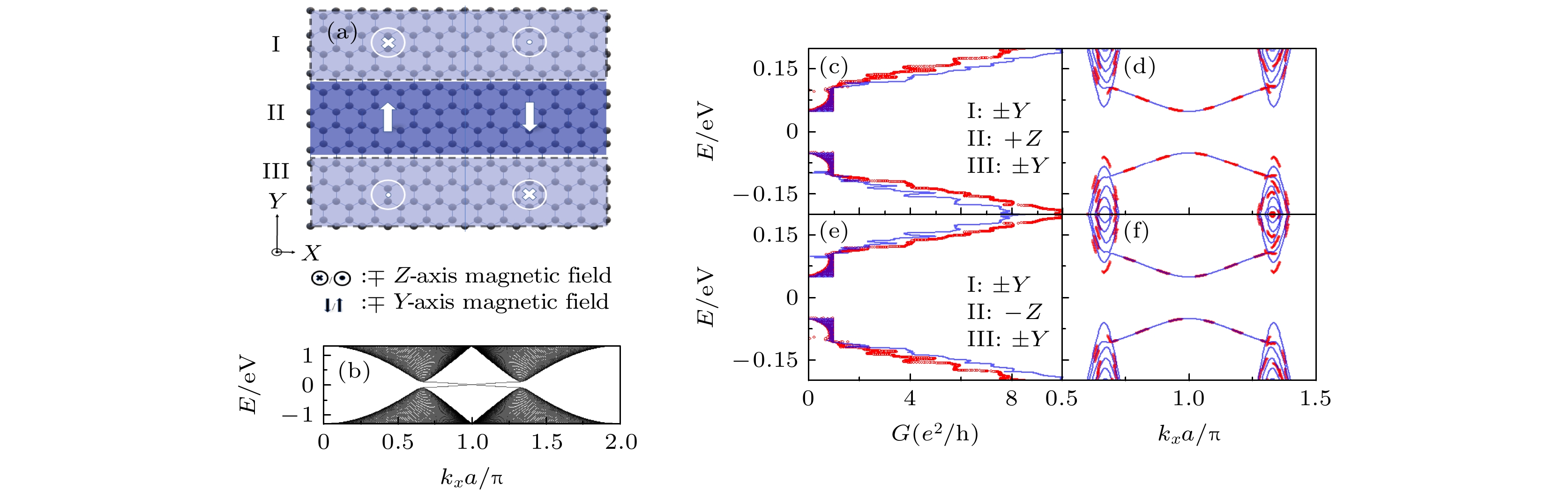
图 1 (a) 交换场作用下的锡烯纳米带俯视图. 图中沿Y轴方向将锡烯等分为I, II, III 3个区域, 并分别对这3个区域施加[I:
$ +Z $ , II:$ +Y $ , III:$ -Z $ ]和[I:$ -Z $ , II:$ -Y $ , III:$ +Z $ ]方向组合的交换场; (b) 无外场作用时锡烯的电子能带结构; 铁磁交换场按照(c) [I:$ \pm Y $ , II:$ +Z $ , III:$ \pm Y $ ]和(e) [I:$ \pm Y $ , II:$ -Z $ , III:$ \pm Y $ ]分布时自旋相关电导随费米能E的变化; (d)交换场强度为$ M=\lambda_{{\rm{so}}}/2 $ , 方向为(d) [I:$ \pm Y $ , II:$ +Z $ , III:$ \pm Y $ ]及(f) [I:$ \pm Y $ , II:$ -Z $ , III:$ \pm Y $ ]时的电子能带结构, 图中红色圈线和蓝色实线分别对应自旋向上和自旋向下的电子Fig. 1. (a) Top view of a stanene nanoribbon with local exchange field, where stanene is equally divided into three regions, (i.e., I, II, and III) along the Y-axis, and exchange fields in the directions of [I:
$ + Z $ , II:$ + Y $ , III:$ - Z $ ] and [I:$ - Z $ , II:$ - Y $ , III:$ + Z $ ] are applied to these three regions respectively. (b) Energy-band diagram of stanene without external field. Spin dependent conductance$ G_\sigma $ as a function of the Fermi energy E with the ferromagnetic exchange fields distributed according to (c) [I:$ \pm Y $ , II:$ + Z $ , III:$ \pm Y $ ] and (e) [I:$ \pm Y $ , II:$ - Z $ , III:$ \pm Y $ ]. Energy-band diagram of stanene with the strength of external field$ M=\lambda_{{\rm{so}}}/2 $ , the exchange field directions are (d) [I:$ \pm Y $ , II:$ +Z $ , III:$ \pm Y $ ] and (f) [I:$ \pm Y $ , II:$ +Z $ , III:$ \pm Y $ ]. The red circle-lines and blue solid-lines correspond to spin-up and spin-down electrons, respectively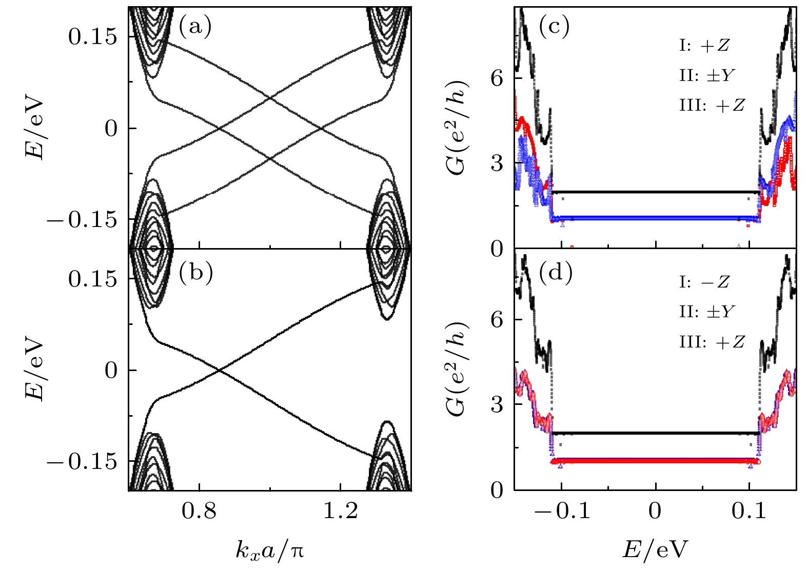
图 2 交换场强度
$M=\lambda_{{\rm{so}}}/2$ , 方向为(a) [I:$ +Z $ , II:$ \pm Y $ , III:$ +Z $ ]及(b) [$ -Z $ , II:$ \pm Y $ , III:$ +Z $ ]时电子能带结构; 交换场按照(c) [I:$ +Z $ , II:$ \pm Y $ , III:$ +Z $ ]和(d) [$ -Z $ , II:$ \pm Y $ , III:$ +Z $ ]分布时电导G随费米能E 的变化, 图中红色圈线、蓝色三角线和黑色点线分别对应自旋向上、自旋向下以及总的电导Fig. 2. Energy-band diagram of stanene with the strength of external field
$ M=\lambda_{{\rm{so}}}/2 $ , the exchange field directions (a) [I:$ +Z $ , II:$ \pm Y $ , III:$ +Z $ ] and (b) [$ -Z $ , II:$ \pm Y $ , III:$ +Z $ ]. Conductance G as a function of the Fermi energy E with the ferromagnetic exchange fields distributed according to (c) [I:$ +Z $ , II:$ \pm Y $ , III:$ +Z $ ] and (d) [$ -Z $ , II:$ \pm Y $ , III:$ +Z $ ]. The red circle-lines, blue triangle-lines and black dot-lines correspond to spin-up, spin-down, and total conductance, respectively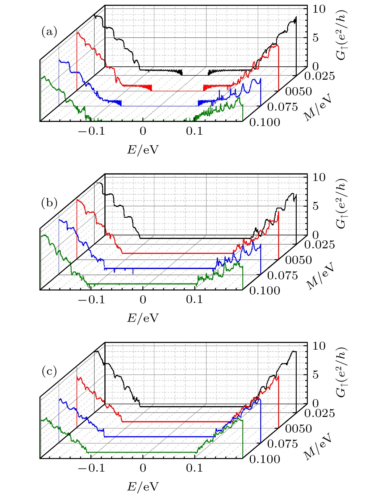
图 3 交换场方向为(a) [I:
$ + Y $ , II:$ + Z $ , III:$ +Y $ ], (b) [I:$ + Z $ , II:$ + Y $ , III:$ +Z $ ], (c) [I:$ - Z $ , II:$ + Y $ , III:$ +Z $ ], 交换场强度参数M分别取0.025, 0.050, 0.075, 0.100 eV 时, 自旋向上电导$ G_\uparrow $ 随费米能E的变化Fig. 3. Conductance G as a function of the Fermi energy E with different values of exchange field parameter
$ M=0.025 $ , 0.050, 0.075, 0.100 eV for the exchange field directions are (a) [I:$ + Y $ , II:$ + Z $ , III:$ +Y $ ], (b) [I:$ + Z $ , II:$ + Y $ , III:$ +Z $ ], (c) [I:$ - Z $ , II:$ + Y $ , III:$ +Z $ ] -
[1] Novoselov K S, Geim A K, Morozov S V, Jiang D, Zhang Y, Dubonos S V, Grigorieva I V, Firsov A A 2004 Science 306 666
Google Scholar
[2] Geim A K, Novoselov K S 2007 Nat. Mater. 6 183
Google Scholar
[3] Chang H, Wang H, Song K K, Zhong M, Shi L B, Qian P 2021 J. Phys.: Condens. Matter 34 013003
[4] Cahangirov S, Topsakal M, Akturk E, Sahin H, Ciraci S 2009 Phys. Rev. Lett. 102 236804
Google Scholar
[5] Sahin H, Cahangirov S, Topsakal M, Bekaroglu E, Ciraci S 2009 Phys. Rev. B 80 155453
Google Scholar
[6] Liu C C, Feng W X, Yao Y G 2011 Phys. Rev. Lett. 107 076802
Google Scholar
[7] Liu C C, Jiang H, Yao Y G 2011 Phys. Rev. B 84 195430
Google Scholar
[8] Xu Y, Yan B H, Zhang H J, Wang J, Xu G, Tang P Z, Duan W H, Zhang S C 2013 Phys. Rev. Lett. 111 136804
Google Scholar
[9] Ni Z, Liu Q, Tang K, Zheng J, Zhou J, Qin R, Gao Z, Yu D, Lu J 2012 Nano Lett. 12 113
Google Scholar
[10] Ezawa M 2013 Appl. Phys. Lett. 102 172103
Google Scholar
[11] Kaneko S, Tsuchiya H, Kamakura Y, Mori N, Ogawa M 2014 Appl. Phys. Express 7 035102
Google Scholar
[12] Ni Z Y, Zhong H X, Jiang X H, Quhe R G, Luo G F, Wang Y Y, Ye M, Yang J B, Shi J J, Lu J 2014 Nanoscale 6 7609
Google Scholar
[13] Zhai X C, Jin G J 2016 J. Phys.: Condens. Matter 28 355002
Google Scholar
[14] Katayama Y, Yamauchi R, Yasutake Y, Fukatsu S, Ueno K 2019 Appl. Phys. Lett. 115 122101
Google Scholar
[15] Zheng J, Xiang Y, Li C L, Yuan R Y, Chi F, Guo Y 2020 Phys. Rev. Appl. 14 034027
Google Scholar
[16] Zheng J, Xiang Y, Li C L, Yuan R Y, Chi F, Guo Y 2021 Phys. Rev. Appl. 16 024046
Google Scholar
[17] Zhu F F, Chen W J, Xu Y, Gao C L, Guan D D, Liu C H, Qian D, Zhang S C, Jia J F 2015 Nat. Mater. 14 1020
Google Scholar
[18] Gou J, Kong L J, Li H, Zhong Q, Li W B, Cheng P, Chen L, Wu K H 2017 Phys. Rev. Mater. 1 054004
Google Scholar
[19] Zang Y Y, Jiang T, Gong Y, Guan Z Y, Liu C, Liao M H, Zhu K J, Li Z, Wang L L, Li W, Song C L, Zhang D, Xu Y, He K, Ma X X, Zhang S C 2018 Adv. Funct. Mater. 28 1802723
Google Scholar
[20] Xu C Z, Chan Y H, Chen P, Wang X X, Flototto D, Hlevyack J A, Bian G, Mo S K, Chou M Y, Chiang T C 2018 Phys. Rev. B 97 035122
Google Scholar
[21] Yuhara J, Fujii Y, Nishino K, Isobe N, Nakatake M, Xian L, Rubio A, Le-Lay G 2018 2D Mater. 5 025002
[22] Deng J L, Xia B Y, Ma X C, Chen H Q, Shan H, Zhai X F, Li B, Zhao A D, Xu Y, Duan W H, Zhang S C, Wang B, Hou J G 2018 Nat. Mater. 17 1081
Google Scholar
[23] Liu Y, Gao N, Zhuang J, Liu C, Wang J, Hao W, Dou S X, Zhao J, Du Y 2019 J. Phys. Chem. Lett. 10 1558
Google Scholar
[24] Pang W, Nishino K, Ogikubo T, Araidai M, Nakatake M, Le Lay G, Yuhara J 2020 Appl. Surf. Sci. 517 146224
Google Scholar
[25] Li J, Lei T, Wang J, Wu R, Qian H, Ibrahim K 2020 Appl. Phys. Lett. 116 101601
Google Scholar
[26] Dhungana D S, Grazianetti C, Martella C, Achilli S, Fratesi G, Molle A 2021 Adv. Funct. Mater. 31 2102797
Google Scholar
[27] Ezawa M 2015 J. Phys. Soc. Jpn. 84 121003
Google Scholar
[28] Wang D, Chen L, Wang X, Cui G, Zhang P 2015 Phys. Chem. Chem. Phys. 17 26979
Google Scholar
[29] Kuang Y D, Lindsay L, Shi S Q, Zheng G P 2016 Nanoscale 8 3760
Google Scholar
[30] van den Broek B, Houssa M, Iordanidou K, Pourtois G, Afanas’ev V V, Stesmans A 2016 2D Mater. 3 015001
[31] Nakamura Y, Zhao T, Xi J, Shi W, Wang D, Shuai Z 2017 Adv. Electron. Mater. 3 1700143
Google Scholar
[32] Shen L, Lan M, Zhang X, Xiang G, 2017 RSC Adv. 7 9840
Google Scholar
[33] Hattori A, Tanaya S, Yada K, Araidai M, Sato M, Hatsugai Y, Shiraishi K, Tanaka Y 2017 J. Phys.: Condens. Matter 29 115302
Google Scholar
[34] Fadaie M, Shahtahmassebi N, Roknabad M R, Gulseren O 2018 Phys. Lett. A 382 180
Google Scholar
[35] Chaves A J, Ribeiro R M, Frederico T, Peres N M R 2017 2D Mater. 4 025086
[36] M. Ezawa 2012 Phys. Rev. B 86 161407
Google Scholar
[37] Salazar C, Muniz R A, Sipe J E 2017 Phys. Rev. Mater. 1 054006
Google Scholar
[38] Rachel S, Ezawa M 2014 Phys. Rev. B 89 195303
Google Scholar
[39] Lado J L, Fernandez-Rossier J 2014 Phys. Rev. Lett. 113 027203
Google Scholar
[40] Li S S, Zhang C W 2016 Mater. Chem. Phys. 173 246
Google Scholar
[41] W. Xiong, C. Xia, T. Wang, Y. Peng, Y. Jia 2016 J. Phys. Chem. C 120 10622
Google Scholar
[42] Krompiewski S, Cuniberti G 2017 Phys. Rev. B 96 155447
Google Scholar
[43] Zhou H, Cai Y, Zhang G, Zhang Y W 2016 Phys. Rev. B 94 045423
Google Scholar
[44] Peng B, Zhang H, Shao H, Xu Y, Ni G, Zhang R, Zhu H 2016 Phys. Rev. B 94 245420
Google Scholar
[45] Peng X F, Zhou X, Jiang X T, Gao R B, Tan S H, Chen K Q 2017 J. Appl. Phys. 122 054302
Google Scholar
[46] Noshin M, Khan A I, Subrina S 2018 Nanotechnology 29 185706
Google Scholar
[47] 郑军, 李春雷, 王小明, 袁瑞旸 2021 物理学报 70 147301
Google Scholar
Zheng J, Li C L, Wang X M, Yuan R Y 2021 Acta Phys. Sin. 70 147301
Google Scholar
[48] Kane C L, Mele E J 2005 Phys. Rev. Lett. 95 146802
Google Scholar
[49] Ezawa M 2012 Phys. Rev. Lett. 109 055502
Google Scholar
[50] Zheng J, Chi F, Guo Y 2018 Appl. Phys. Lett. 113 112404
Google Scholar
[51] Zheng J, Chi F, Guo Y 2018 Phys. Rev. Appl. 9 024012
Google Scholar
[52] Haldane F D M 1988 Phys. Rev. Lett. 61 2015
Google Scholar
[53] Kane C L, Mele E J 2005 Phys. Rev. Lett. 95 226801
Google Scholar
[54] Williams J R, Carlo L D, Marcus C M 2007 Science 317 638
Google Scholar
[55] Pastawski H M 1991 Phys. Rev. B 44 6329
Google Scholar
[56] Datta S 1992 Phys. Rev. B 45 1347
[57] Lee D H, Joannopoulos J D 1981 Phys. Rev. B 23 4997
Google Scholar
[58] Sancho M P L, Sancho J M L, Rubio J 1984 J. Phys. F: Met. Phys. 14 1205
Google Scholar
[59] Sancho M P L, Sancho J M L, Sancho J M L, Rubio J 1985 J. Phys. F: Met. Phys. 15 851
Google Scholar


 下载:
下载:


计量
- 文章访问数: 6438
- PDF下载量: 101
- 被引次数: 0
