


-
整流器件是微波无线能量传输系统的核心部分, 新型整流器件的研发是当前领域研究的重要方向. 肖特基二极管和场效应晶体管是目前主流整流器件, 但二者整流范围有限, 无法实现兼顾弱能量和中等能量密度的宽范围整流. 有鉴于此, 本文提出并设计了2.45 GHz微波无线能量传输用Ge基p型单端肖特基势垒场效应晶体管(源端为肖特基接触, 漏端为标准p+掺杂). 在此基础上, 充分利用器件的肖特基结构, 采用新型二极管连接方式, 以实现不同偏压下开启的沟道和源衬肖特基结构的双通道宽范围整流. 采用Silvaco TCAD软件进行仿真, 对于负载为0.3 pF和70 kΩ的半波整流电路, 实现了–20—24 dBm宽范围整流, 相比同条件下Ge场效应晶体管范围拓宽8 dBm, 且在范围内整体整流效率较高, 在16 dBm整流效率峰值可达57.27%. 在–10 dBm弱能量密度的整流效率达到6.17%, 是同等条件下Ge 场效应晶体管的7倍多.
-
关键词:
- 无线能量传输 /
- 肖特基势垒场效应晶体管 /
- 肖特基接触 /
- 整流效率
Rectifier component is a core part of a microwave wireless energy transmission system, and the development of new rectifier components is an important research direction in this field. Schottky diodes and field-effect transistors are currently the mainstream rectifier devices, but they have a limited rectification range and cannot achieve a wide-range rectification of both weak energy and medium energy density at the same time. In view of this, in this work proposed and designed is a Ge based p-type single-ended Schottky barrier field effect transistor (Schottky contact at the source and standard p+ doping at the drain) for 2.45 GHz microwave wireless energy transmission. Based on this, the Schottky structure of the device is fully utilised and a new diode connection is used in order to realize a dual channel wide range rectification of the trench and source lined Schottky structure opened at different bias voltages. Simulations are carried out by using the Silvaco TCAD software. For a half-wave rectifier circuit with a load of 0.3 pF and 70 kΩ, a wide range from –20 to 24 dBm rectification is achieved, which is 8 dBm wider than the range of Ge field-effect transistors under the same conditions, and the overall rectification efficiency is higher in the range, with a peak rectification efficiency of 57.27% at 16 dBm. The rectification efficiency at –10 dBm weak energy density reaches 6.17%, which is more than 7 times that of Ge FETs under the same conditions.-
Keywords:
- wireless energy transmission /
- Schottky barrier field effect transistor /
- Schottky contact /
- rectifying efficiency
[1] Ullah M A, Keshavarz R, Abolhasan M, Lipman J, Esselle K P, Shariati N 2022 IEEE Access 10 17231
 Google Scholar
[2] Haerinia M, Shadid R 2020 Signals 1 209
Google Scholar
[3] Divakaran S K, Krishna D D 2019 INT. J. RF. Microw. C. E 29 e21633
Google Scholar
[4] Zhang Z, Pang H, Georgiadis A, Cecati C 2019 IEEE Trans. Ind. Electron. 66 1044
Google Scholar
[5] Eteng A A, Goh H H, Rahim S K A, Alomainy A 2021 IEEE Access 9 27518
Google Scholar
[6] Zhu G L, Du J X, Yang X X, Zhou Y G, Gao S 2019 IEEE Access 7 141978
Google Scholar
[7] Xiao H, Zhang H, Song W, Wang J, Chen W, Lu M 2021 IEEE Trans. Ind. Electron. 69 2896
Google Scholar
[8] 宋建军, 张龙强, 陈雷, 周亮, 孙雷, 兰军峰, 习楚浩, 李家豪 2021 物理学报 70 108401
Google Scholar
Song J J, Zhang L Q, Chen L, Zhou L, Sun L, Lan J F, Xi C H, Li J H 2021 Acta Phys. Sin. 70 108401
Google Scholar
[9] 李妤晨, 陈航宇, 宋建军 2020 物理学报 69 108401
Google Scholar
Li Y C, Chen H Y, Song J J 2020 Acta Phys. Sin. 69 108401
Google Scholar
[10] Chong G, Ramiah H, Yin J, Rajendran J, Mak P I, Martins R P 2019 IEEE Trans. Circuits Syst. II, Exp. Briefs 68 1743
Google Scholar
[11] Choi W, Lee J, Shin M 2014 IEEE Trans. Electron Devices 61 37
Google Scholar
[12] Kim S, Lee K, Lee J H, Park B G, Kwon D 2021 IEEE Trans. Electron Devices 68 4754
Google Scholar
[13] Yao Y, Sun Y, Li X, Shi Y, Liu Z 2020 IEEE Trans. Electron Devices 67 751
Google Scholar
[14] Chen C W, Tzeng J Y, Chuang C T, Chien H P, Chien C H, Luo G L 2014 IEEE Trans. Electron Devices 61 2656
Google Scholar
[15] 张茂添 2014 硕士学位论文 (厦门: 厦门大学)
Zhang M T 2014 M. S. Thesis (Xiamen: Xiamen University) (in Chinese)
[16] 施敏, 伍国珏(耿莉, 张瑞智译) 2007 半导体器件物理 (北京: 西安交通大学出版社) 第 130—142页
Sze S M, Kwok K N (translated by Geng L, Zhang R Z) 2007 Physics of Semiconductor Devices (Xi’an: Xi’an jiaotong University Press) pp130–142 (in Chinese)
[17] 汤晓燕 2007博士学位论文 (西安: 西安电子科技大学)
Tang X Y 2007 Ph. D. Dissertation (Xi’an: Xidian University) (in Chinese)
[18] Shokrani M R, Hamidon M N, Khoddam M, Najafi V 2012 IEEE International Conference on Electronics Design Kuala Lumpur, Malaysia, November 5–6, 2012 p234
[19] Shokrani M R, Khoddam M, Hamidon M N B, Kamsani N A, Rokhani F Z, Shafie S B 2014 Sci. World J. 2014 1
Google Scholar
[20] Zhang D, Song J J, Xue X H, Zhang S Q 2022 Chin. Phys. B 31 068401
Google Scholar
-
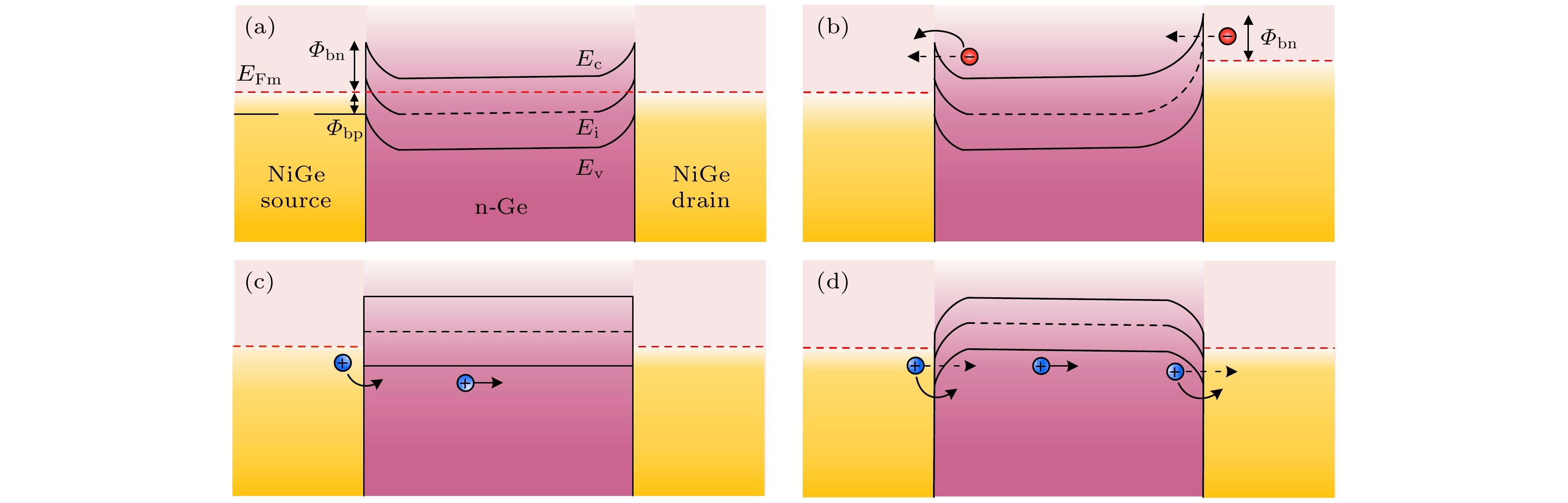
图 1 Ge基p沟SB-MOSFET随外加电压变化的能带图 (a)
$| {{V_{\text{g}}}} | = | {{V_{\text{d}}}} | = 0$ ; (b)$| {{V_{\text{g}}}} | = 0, | {{V_{\text{d}}}} | > 0$ ; (c)$ | {{V_{\text{g}}}} | < | {{V_{\text{T}}}} | $ ; (d)$| {{V_{\text{g}}}} | > | {{V_{\text{T}}}} |$ Fig. 1. Energy band diagram of Ge based p-channel SB-MOSFET with applied voltage: (a)
$ | {{V_{\text{g}}}} | = | {{V_{\text{d}}}} | = 0 $ ; (b)$ | {{V_{\text{g}}}} | = 0, | {{V_{\text{d}}}} | > 0 $ ; (c)$ | {{V_{\text{g}}}} | < | {{V_{\text{T}}}} | $ ; (d)$ | {{V_{\text{g}}}} | > | {{V_{\text{T}}}} | $ .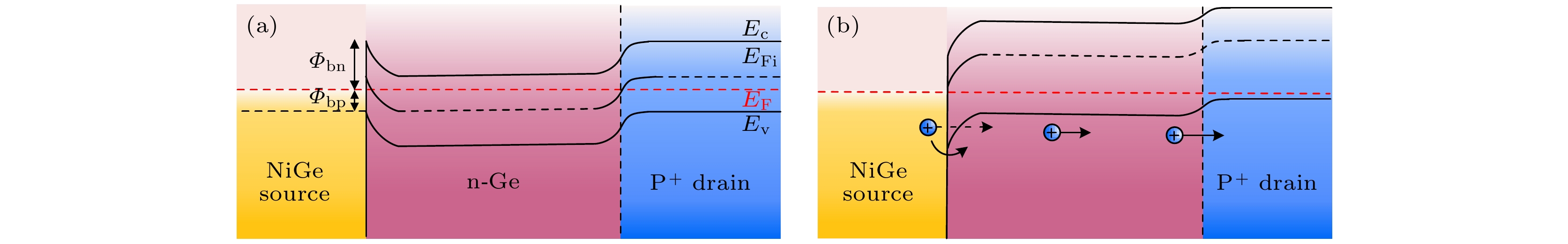
图 2 Ge基p沟SBSL-MOSFET随外加电压变化的能带图 (a)
$ \left| {{V_{\text{g}}}} \right| = \left| {{V_{\text{d}}}} \right| = 0 $ ; (b)$ \left| {{V_{\text{g}}}} \right| > \left| {{V_{\text{T}}}} \right| $ Fig. 2. Energy band diagram of Ge based p-channel SBSL-MOSFET with applied voltage: (a)
$ \left| {{V_{\text{g}}}} \right| = \left| {{V_{\text{d}}}} \right| = 0 $ ; (b)$ \left| {{V_{\text{g}}}} \right| > \left| {{V_{\text{T}}}} \right| $ .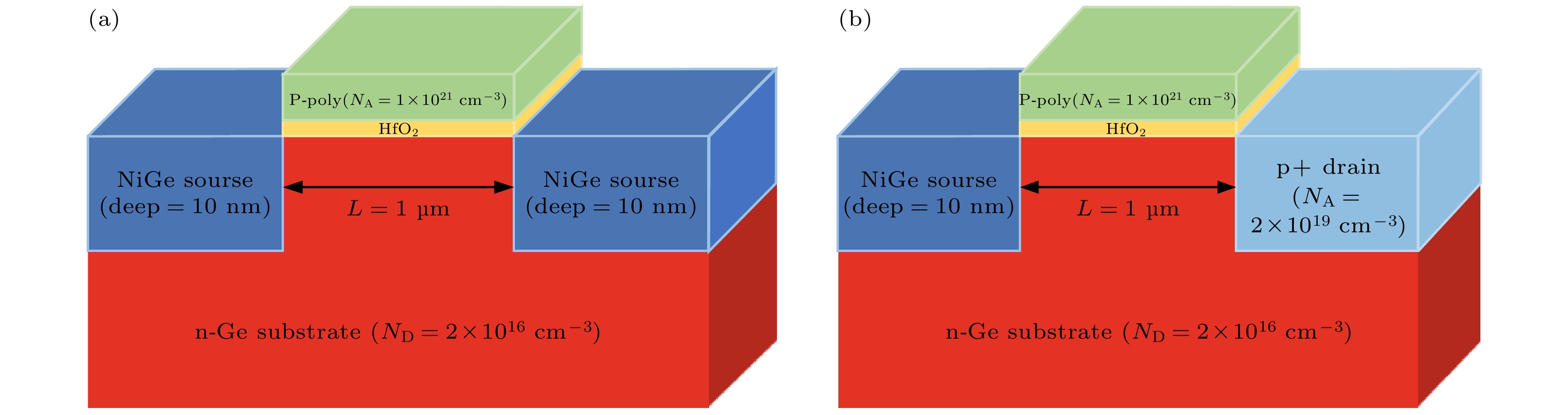
图 3 SB-MOSFET (a) 和 SBSL-MOSFET (b)器件结构及仿真用关键参数值
Fig. 3. The key parameter values for device structure and simulation of SB-MOSFET (a) and SBSL-MOSFET (b).
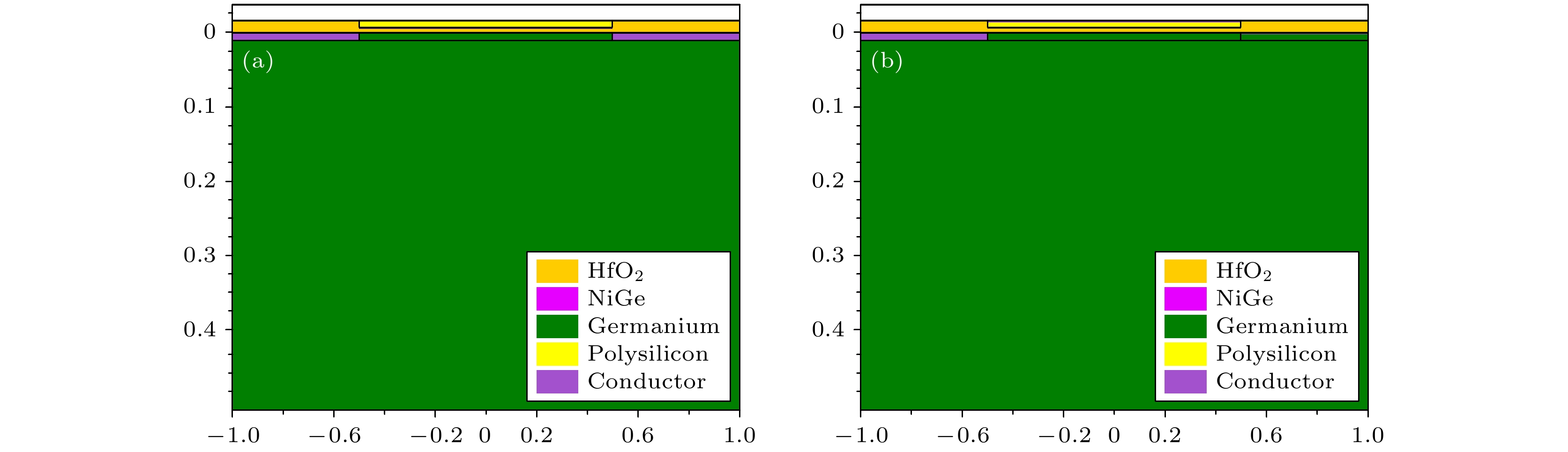
图 4 Ge SB-MOSFET (a)和 Ge SBSL-MOSFET (b)仿真结构图
Fig. 4. The simulation structure diagram of Ge SB-MOSFET (a) and SBSL-MOSFET (b).

图 5 标准坐标系(a)和对数坐标系下(b)三种MOSFET的转移特性曲线图
Fig. 5. Transfer characteristic curves of three MOSFETs in the standard coordinate system (a) and the logarithmic coordinate system (b).
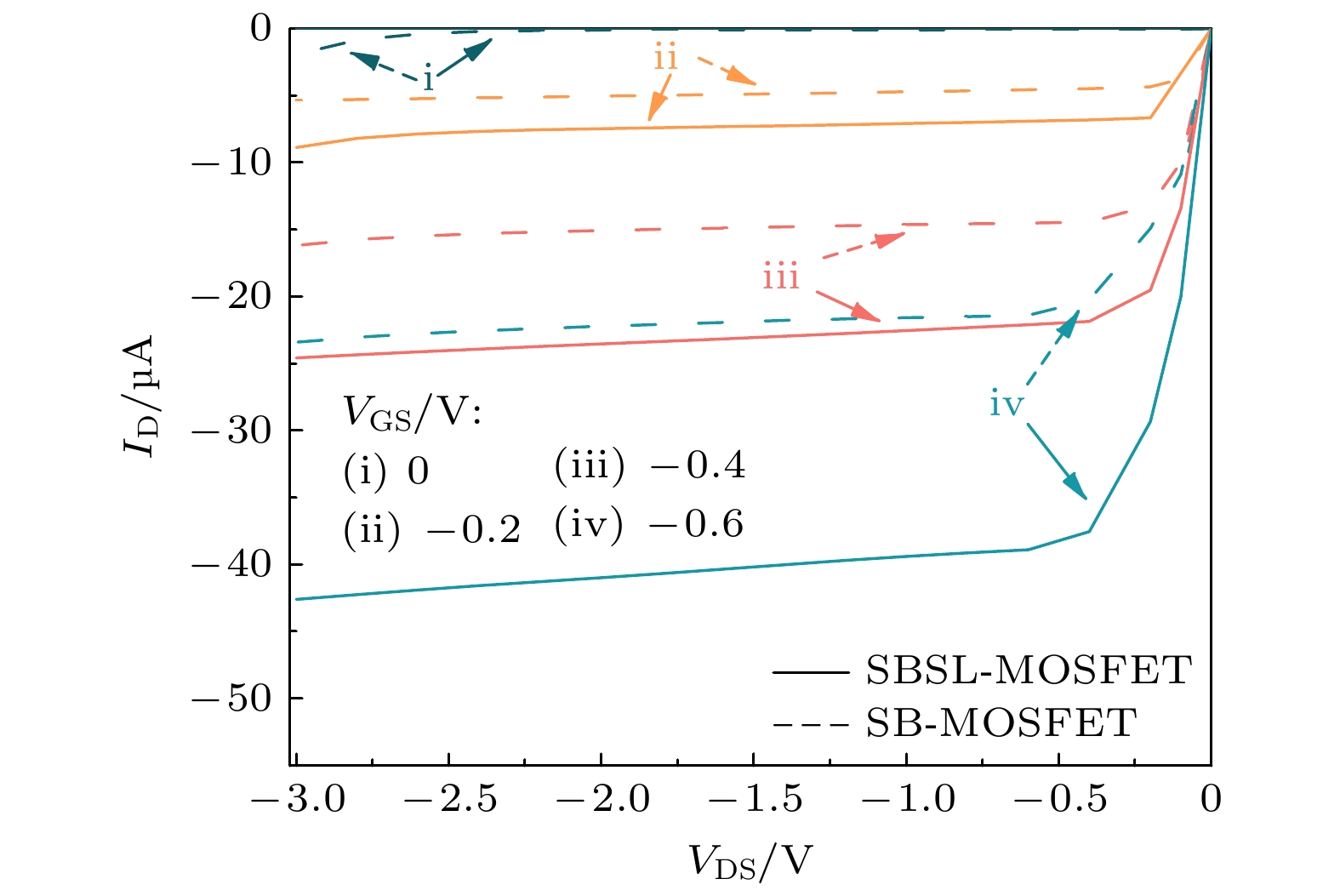
图 6 SB-MOSFET和SBSL-MOSFET输出特性曲线图
Fig. 6. Output characteristic curves of SB-MOSFET and SBSL-MOSFET.
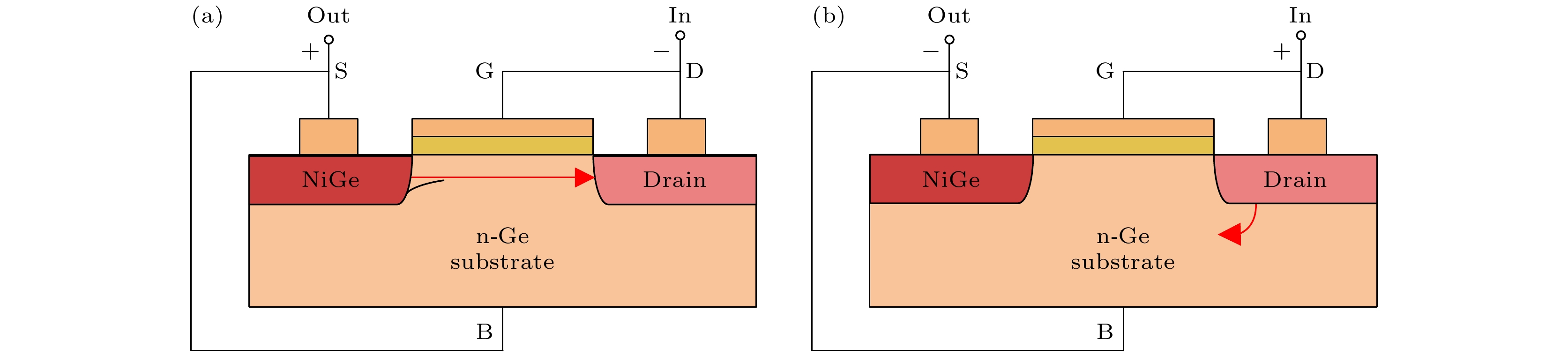
图 8 传统二极管连接方式SBSL-MOSFET电流示意图 (a) 正向电流; (b) 反向电流
Fig. 8. Conventional diode connection of SBSL-MOSFET current diagram: (a) Forward current; (b) reverse current.
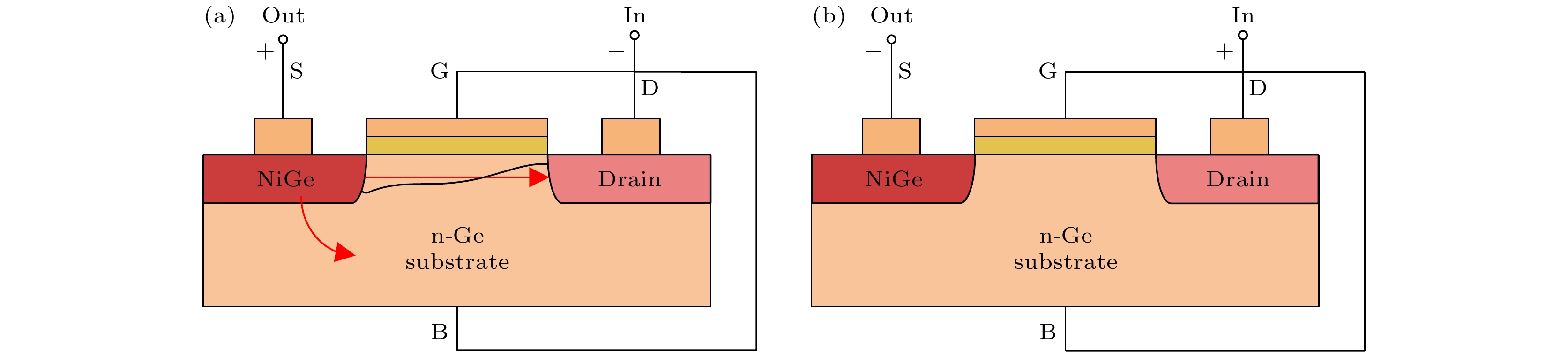
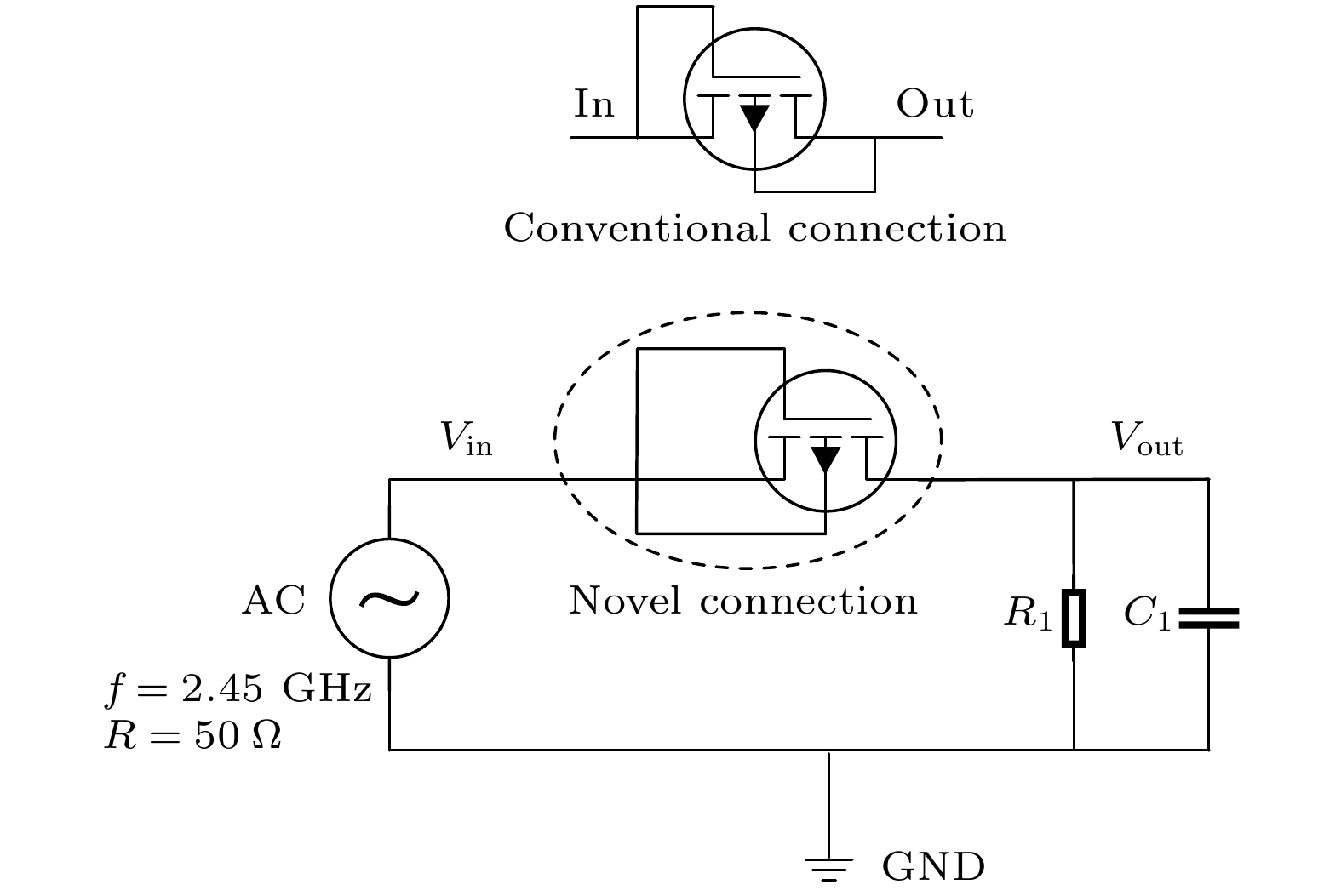
图 9 新型连接方式SBSL-MOSFET电流示意图 (a) 正向电流; (b) 反向电流
Fig. 9. Novel connection of SBSL-MOSFET current diagram: (a) Forward current; (b) reverse current.
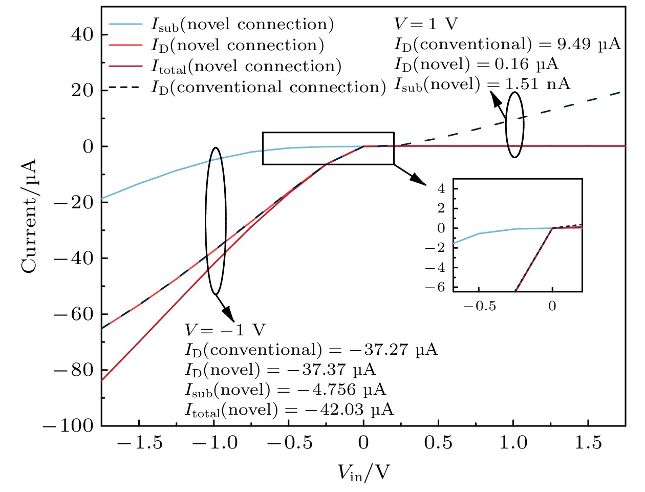
图 11 Ge基SBSL-MOSFET在两种连接方式下的I-V曲线图
Fig. 11. I-V curve diagram under two connection methods of Ge based SBSL-MOSFET.
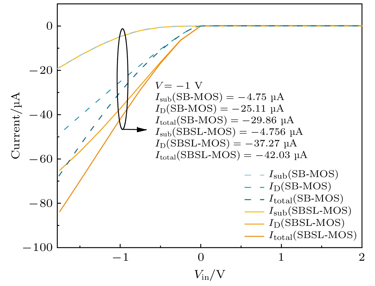
图 12 SB-MOSFET和SBSL-MOSFET在新型连接方式下I-V曲线图
Fig. 12. I-V curve diagram under the new connection method of SB-MOSFET and SBSL-MOSFET.
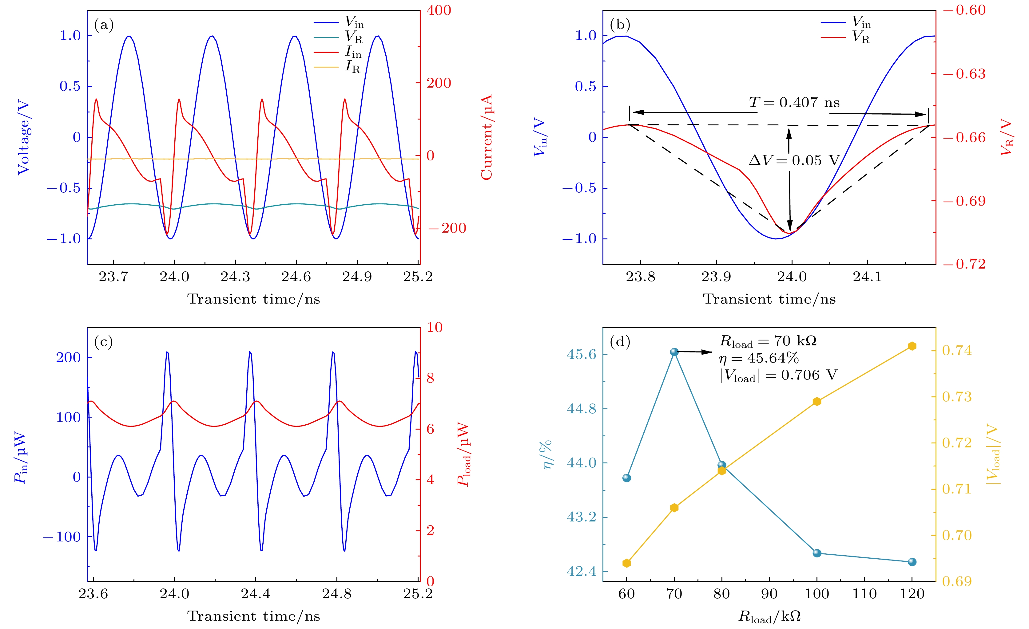
图 13 (a) 瞬态仿真输入输出电流电压波形图; (b) 瞬态仿真输入输出电压单周期局部放大图; (c) 瞬态仿真输入输出功率图; (d) 整流效率和负载电压随负载阻抗变化图
Fig. 13. (a) Transient simulation input and output current and voltage waveforms; (b) transient simulation input and output voltage single-cycle partial enlarged diagram; (c) transient simulation input and output power diagrams; (d) rectification efficiency and load voltage with load impedance change graph.
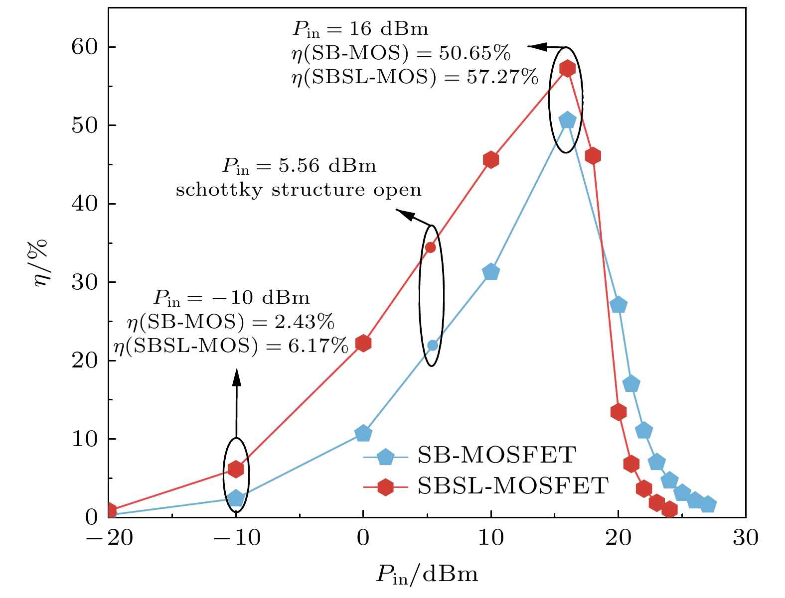
图 14 SB-MOSFET和SBSL-MOSFET整流效率曲线图
Fig. 14. Rectifying efficiency graph of SB-MOSFET and SBSL-MOSFET.
-
[1] Ullah M A, Keshavarz R, Abolhasan M, Lipman J, Esselle K P, Shariati N 2022 IEEE Access 10 17231
Google Scholar
[2] Haerinia M, Shadid R 2020 Signals 1 209
Google Scholar
[3] Divakaran S K, Krishna D D 2019 INT. J. RF. Microw. C. E 29 e21633
Google Scholar
[4] Zhang Z, Pang H, Georgiadis A, Cecati C 2019 IEEE Trans. Ind. Electron. 66 1044
Google Scholar
[5] Eteng A A, Goh H H, Rahim S K A, Alomainy A 2021 IEEE Access 9 27518
Google Scholar
[6] Zhu G L, Du J X, Yang X X, Zhou Y G, Gao S 2019 IEEE Access 7 141978
Google Scholar
[7] Xiao H, Zhang H, Song W, Wang J, Chen W, Lu M 2021 IEEE Trans. Ind. Electron. 69 2896
Google Scholar
[8] 宋建军, 张龙强, 陈雷, 周亮, 孙雷, 兰军峰, 习楚浩, 李家豪 2021 物理学报 70 108401
Google Scholar
Song J J, Zhang L Q, Chen L, Zhou L, Sun L, Lan J F, Xi C H, Li J H 2021 Acta Phys. Sin. 70 108401
Google Scholar
[9] 李妤晨, 陈航宇, 宋建军 2020 物理学报 69 108401
Google Scholar
Li Y C, Chen H Y, Song J J 2020 Acta Phys. Sin. 69 108401
Google Scholar
[10] Chong G, Ramiah H, Yin J, Rajendran J, Mak P I, Martins R P 2019 IEEE Trans. Circuits Syst. II, Exp. Briefs 68 1743
Google Scholar
[11] Choi W, Lee J, Shin M 2014 IEEE Trans. Electron Devices 61 37
Google Scholar
[12] Kim S, Lee K, Lee J H, Park B G, Kwon D 2021 IEEE Trans. Electron Devices 68 4754
Google Scholar
[13] Yao Y, Sun Y, Li X, Shi Y, Liu Z 2020 IEEE Trans. Electron Devices 67 751
Google Scholar
[14] Chen C W, Tzeng J Y, Chuang C T, Chien H P, Chien C H, Luo G L 2014 IEEE Trans. Electron Devices 61 2656
Google Scholar
[15] 张茂添 2014 硕士学位论文 (厦门: 厦门大学)
Zhang M T 2014 M. S. Thesis (Xiamen: Xiamen University) (in Chinese)
[16] 施敏, 伍国珏(耿莉, 张瑞智译) 2007 半导体器件物理 (北京: 西安交通大学出版社) 第 130—142页
Sze S M, Kwok K N (translated by Geng L, Zhang R Z) 2007 Physics of Semiconductor Devices (Xi’an: Xi’an jiaotong University Press) pp130–142 (in Chinese)
[17] 汤晓燕 2007博士学位论文 (西安: 西安电子科技大学)
Tang X Y 2007 Ph. D. Dissertation (Xi’an: Xidian University) (in Chinese)
[18] Shokrani M R, Hamidon M N, Khoddam M, Najafi V 2012 IEEE International Conference on Electronics Design Kuala Lumpur, Malaysia, November 5–6, 2012 p234
[19] Shokrani M R, Khoddam M, Hamidon M N B, Kamsani N A, Rokhani F Z, Shafie S B 2014 Sci. World J. 2014 1
Google Scholar
[20] Zhang D, Song J J, Xue X H, Zhang S Q 2022 Chin. Phys. B 31 068401
Google Scholar


 下载:
下载:


计量
- 文章访问数: 7518
- PDF下载量: 81
- 被引次数: 0
