


-
在实际静电放电测试时, 发现各种功率金属-氧化物半导体场效应晶体管(MOSFET)的静电放电测试结果均呈现出正反向耐压不对称现象, 而人体与器件接触时的静电放电过程是不区分正反向的. 正反向耐压差异较大对于功率MOSFET或作为静电放电保护器件来说都是无法接受的, 其造成器件失效的问题格外凸显. 本文通过建立SGT-MOSFET, VUMOSFET和VDMOS在静电放电正反向电压下的栅源电容解析模型, 对比分析了三种功率MOSFET器件静电放电正反向耐压不对称及其比值不同的原因, 为器件的静电放电测试及可靠性分析提供了理论依据.
-
关键词:
- 功率金属-氧化物半导体场效应晶体管 /
- 静电放电 /
- 栅源电容 /
- 解析模型
In the actual human body model (HBM) test, it is found that the electrostatic discharge (ESD) test results of various power metal-oxide-semiconductor field-effect transistor (MOSFET) devices show asymmetry between forward withstand voltage and reverse withstand voltage, while the ESD process does not distinguish between positive direction and negative direction. Large differences between forward and reverse withstand voltages are unacceptable for power MOSFETs or as ESD protection devices. The problem of its causing device failure is particularly pronounced. In this work, by establishing the analytical model of gate-to-source capacitance of SGT-MOSFET, VUMOSFET and VDMOS under the forward and reverse voltages, we comparatively analyze the reasons for the asymmetry of the forward and reverse withstand voltages and their different ratios of the three kinds of power MOSFETs, which provides a theoretical basis for testing the device’s ESD and the analyzing their reliability. It is found that the ESD forward and reverse withstand voltage asymmetry phenomena of different power MOSFET structures are related to the variation of gate-to-source capacitance, caused by the reverse-type layer. When a forward voltage is applied across the gate and source, the device gate-to-source capacitance consists of the oxide layer capacitance around the gate in parallel; when a reverse voltage is applied, the gate-to-source capacitance consists of the virtual gate-to-drain capacitance in series with the inverse layer capacitance and then in parallel with the other oxide layer capacitance around the gate. This results in a decrease of the gate-to-source capacitance at the reverse voltage, making the device reverse withstand voltage greater than the forward withstand voltage. The difference in the ratio of ESD reverse withstand voltage to forward withstand voltage among different devices is related to the change of the capacitance of the inverse layer in the gate-to-source capacitor under reverse voltage caused by the difference in device structure.[1] Jung D Y, Park K S, Kim S I, Kwon S, Cho D H, Jang H G, Lim J W 2023 ETRI J. 45 543
 Google Scholar
[2] Mai X C, Chen S L, Chen H W, Lee Y M 2023 Electronics 12 2803
Google Scholar
[3] Yan Y, Lan W, Chen Y, Yang D, Zhou Y, Zhu Z, Liou J J 2022 Adv. Electron. Mater. 8 2100886
[4] Anderson N T, Lockledge S P 2022 ASM International Pasadena, USA, October 30–November 3, 2022 pp329–332
[5] Smallwood J M 2023 J. Electrostat. 125 103817
Google Scholar
[6] Ker M D, Pommerenke D 2022 IEEE Trans. on Electromagn. Compat. 64 1783
Google Scholar
[7] Yang L, Yang C, Tu Y, Wang X, Wang Q 2021 IEEE Access 9 33512
Google Scholar
[8] Ji Q, Luo A, Liu Q, Wan B 2023 International Conference on Optoelectronic Information and Functional Materials 2023 12781
[9] Gimenez S P, Galembeck E H S 2023 ECS Trans. 111 161
Google Scholar
[10] Ajay 2021 Silicon 13 1325
Google Scholar
[11] Hong S Z, Chen S L, Chen H W, Lee Y M 2021 IEEE Electron Device Lett. 42 1512
Google Scholar
[12] Lai J Y, Chen S L, Liu Z W, Chen H W, Chen H H, Lee Y M 2022 Sens. Mater. 34 1835
[13] Zhu Z, Yang Z, Fan X, W Fan 2021 Crystals 11 128
Google Scholar
[14] Luo X, Xu J, Xu X, Luo H, Dai Z 2022 2022 International EOS/ESD Symposium on Design and System Chengdu China, November 9–11, 2022 p2023-03-22
[15] Arosio M, Boffino C, Morini S, Dirk Priefert, Oezguer Albayrak, Viktor Boguszewicz, Andrea Baschirotto 2021 IEEE Trans Electron. Devices 68 2848
Google Scholar
[16] 苏乐, 王彩琳, 杨武华, 梁晓刚, 张超 2023 物理学报 72 148501
Google Scholar
Su L, Wang C L, Yang W H, Liang X G, Zhang C 2023 Acta Phys. Sin. 72 148501
Google Scholar
[17] Xi J, Wang J, Lu J, Chen J, Xin Y, Li Z, Tu C, Shen Z J 2018 Microelectron. Reliab. 88-90 593
Google Scholar
[18] Su L, Wang C L, Yang W H, Zhang C 2023 Microelectron. Reliab. 143 114950
Google Scholar
[19] Tian Y, Yang Z, Xu Z, Liu S, Sun W F, Shi L, Zhu Y, Ye P, Zhou J 2018 Superlattices Microstruct. 116 151
Google Scholar
[20] Su L, Wang C L, Yang W H, An J 2022 Microelectron. Reliab. 139 114822
Google Scholar
[21] Sun J, Zheng Z, Zhang L, Chen K J 2022 2022 IEEE 34th International Symposium on Power Semiconductor Devices and ICS Vancouver, Canada, May 22–25, 2022 pp73–76
-
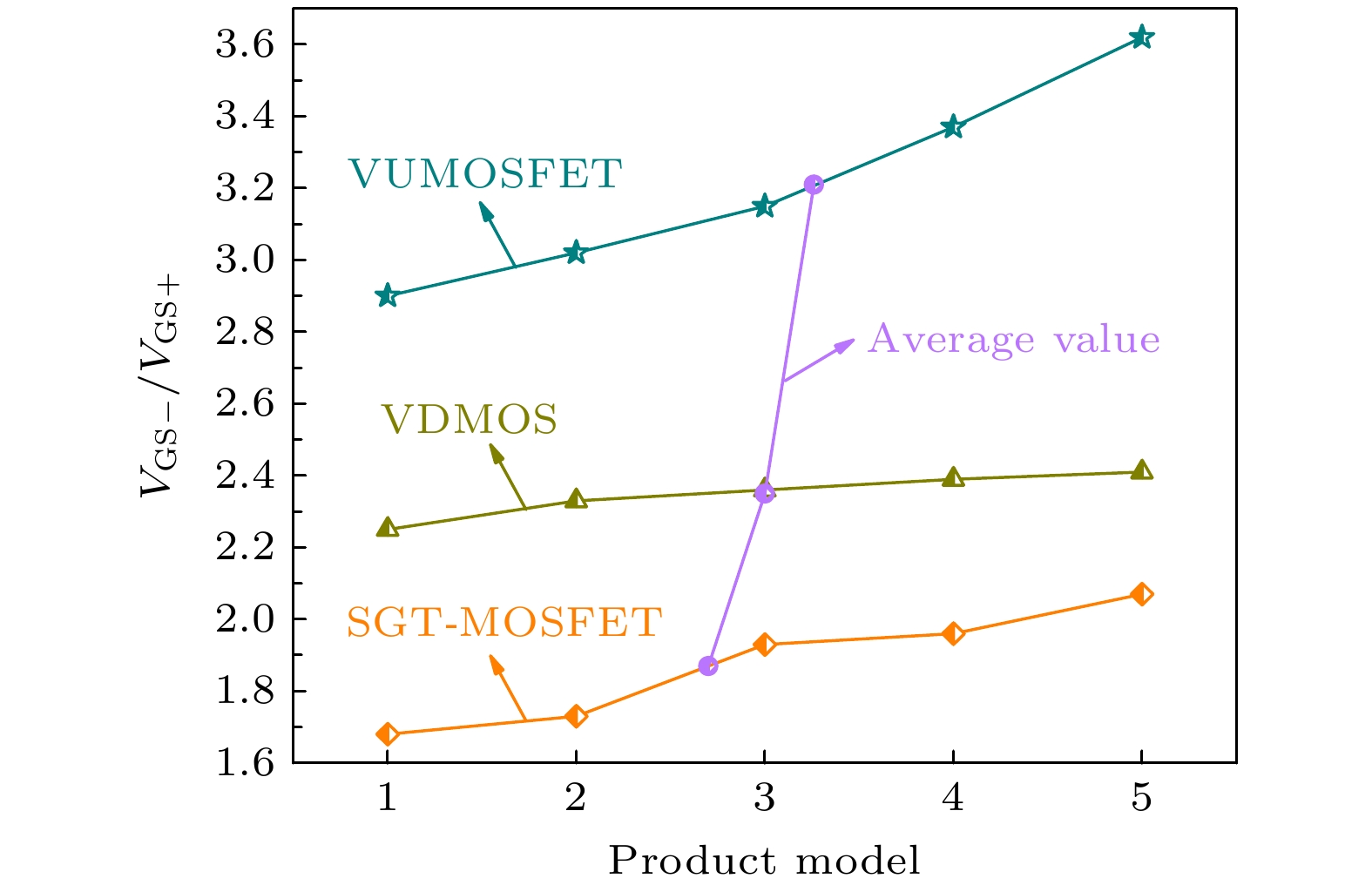
图 1 SGT-MOSFET, VUMOSFET, VDMOS产品HBM测试的反向耐压与正向耐压比值
Fig. 1. The positive and negative pass voltage difference multiple of SGT-MOSFET, VUMOSFET, and VDMOS under HBM testing
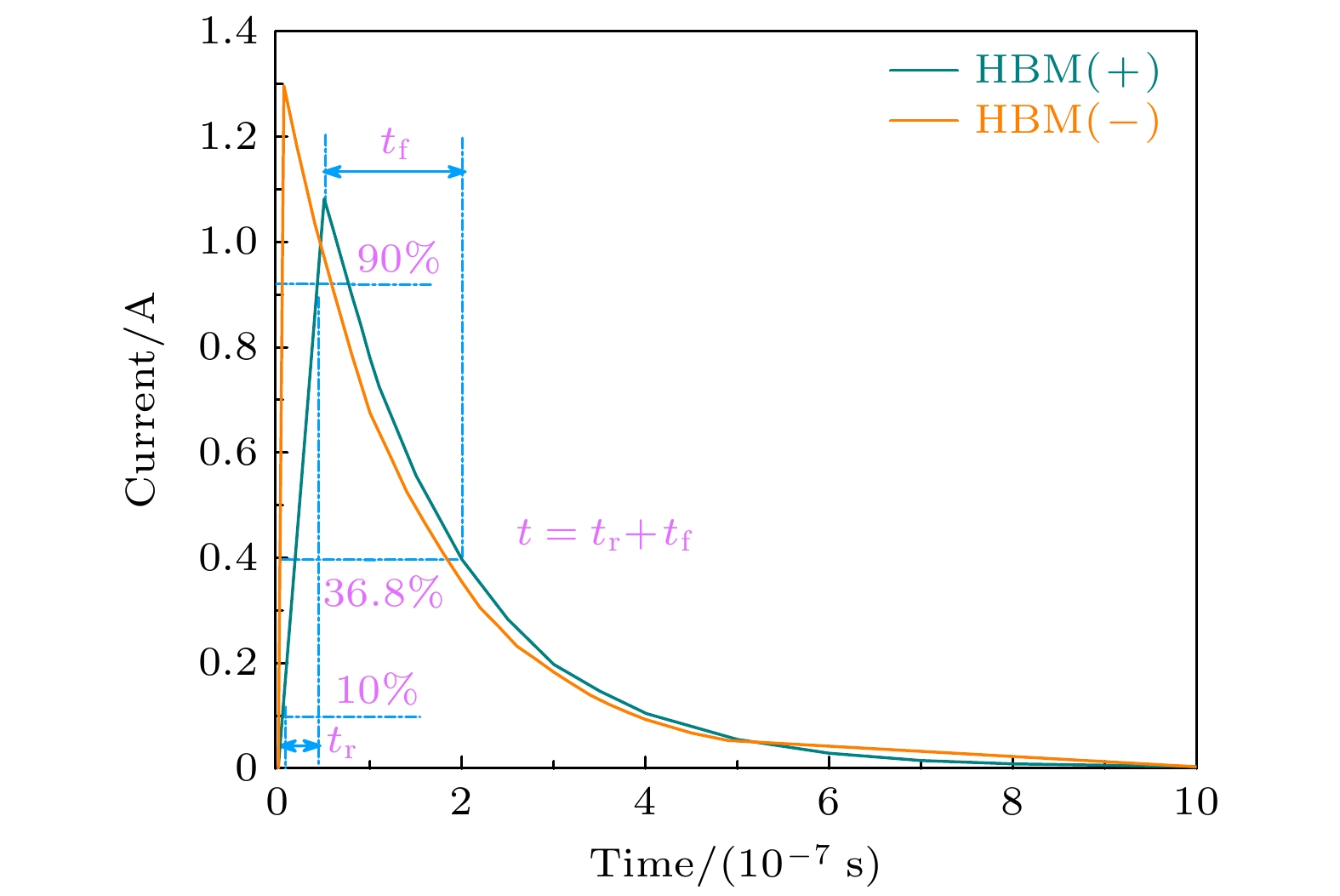
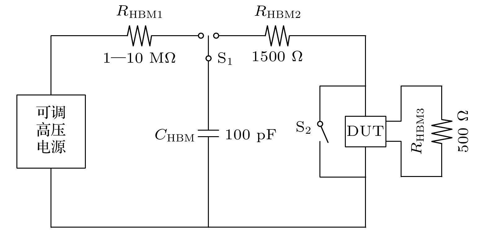
图 3 SGT-MOSFET在HBM模型下的放电波形 (RHBM1 = 1 MΩ, RHBM2 = 1500 Ω, RHBM3 = 500 Ω, CHBM = 100 pF)
Fig. 3. The discharge waveform of SGT-MOSFET under the HBM model (RHBM1 = 1 MΩ, RHBM2 = 1500 Ω, RHBM3 = 500 Ω, CHBM = 100 pF).
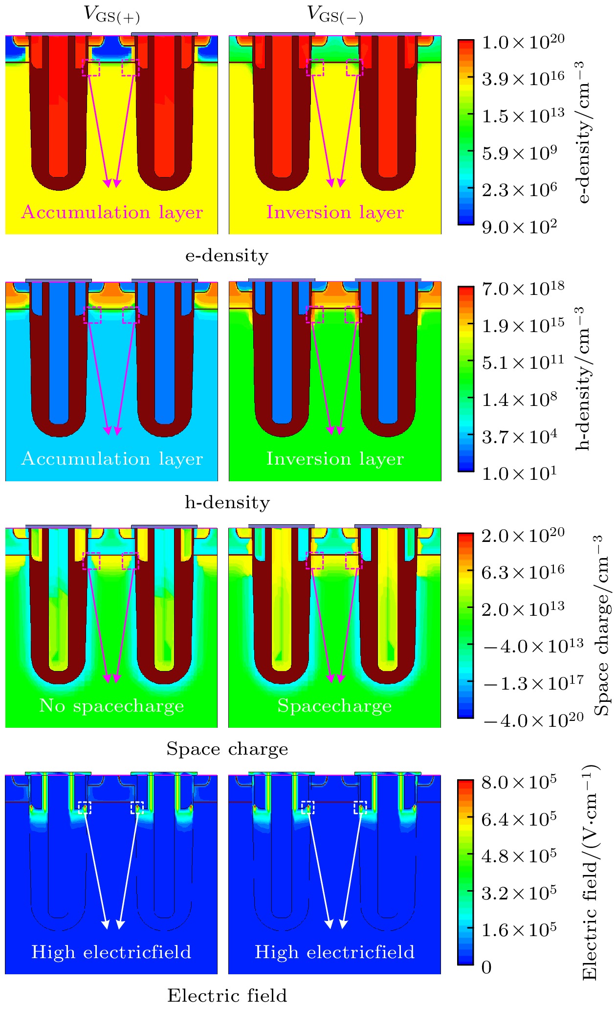
图 4 SGT-MOSFET ESD正反向电压下的电子密度、空穴密度、空间电荷及电场强度分布图
Fig. 4. The e-density, h-density, space charge, and electric field distribution diagram of SGT-MOSFET under forward and reverse voltage of ESD.
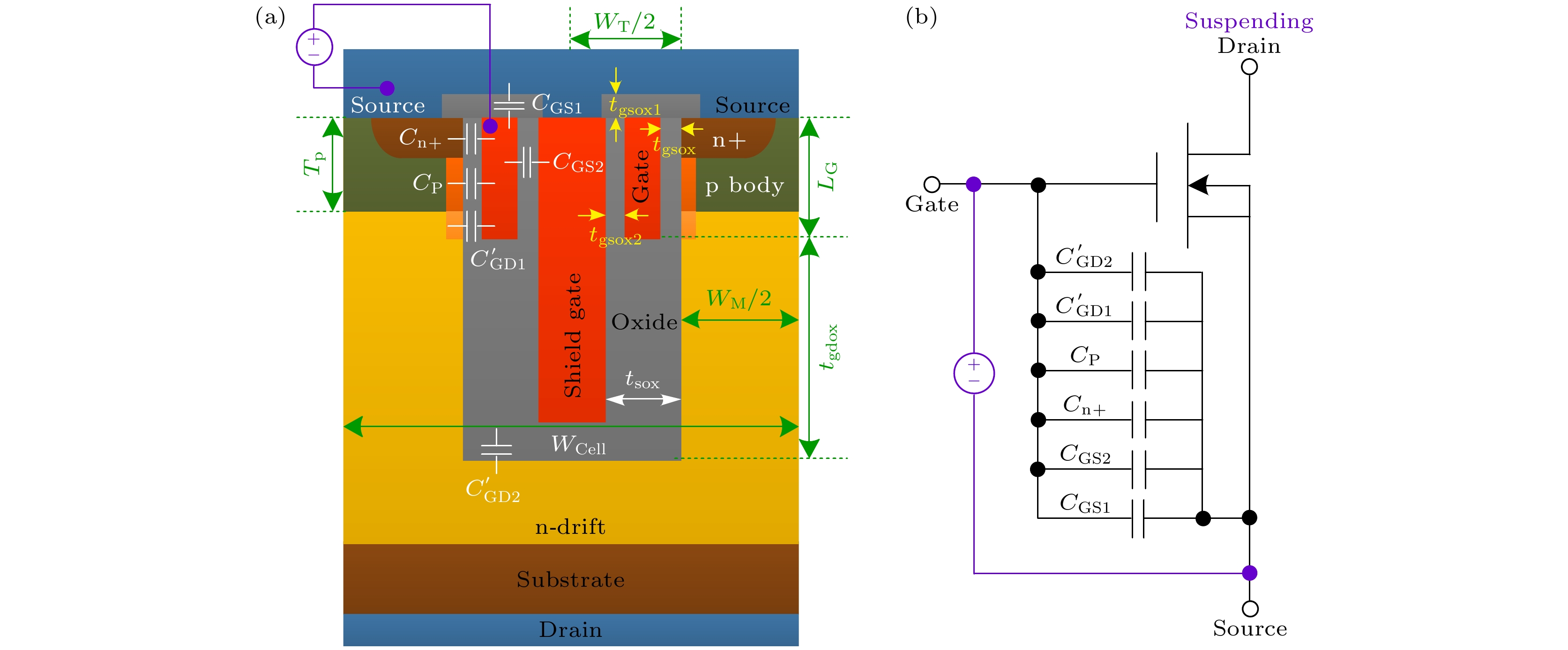
图 5 SGT-MOSFET正向耐压测试下的栅源电容CGS(+) (a)及等效电路(b)示意图
Fig. 5. Schematic diagram of SGT-MOSFET gate to source capacitor CGS(+) (a) and equivalent circuit (b).
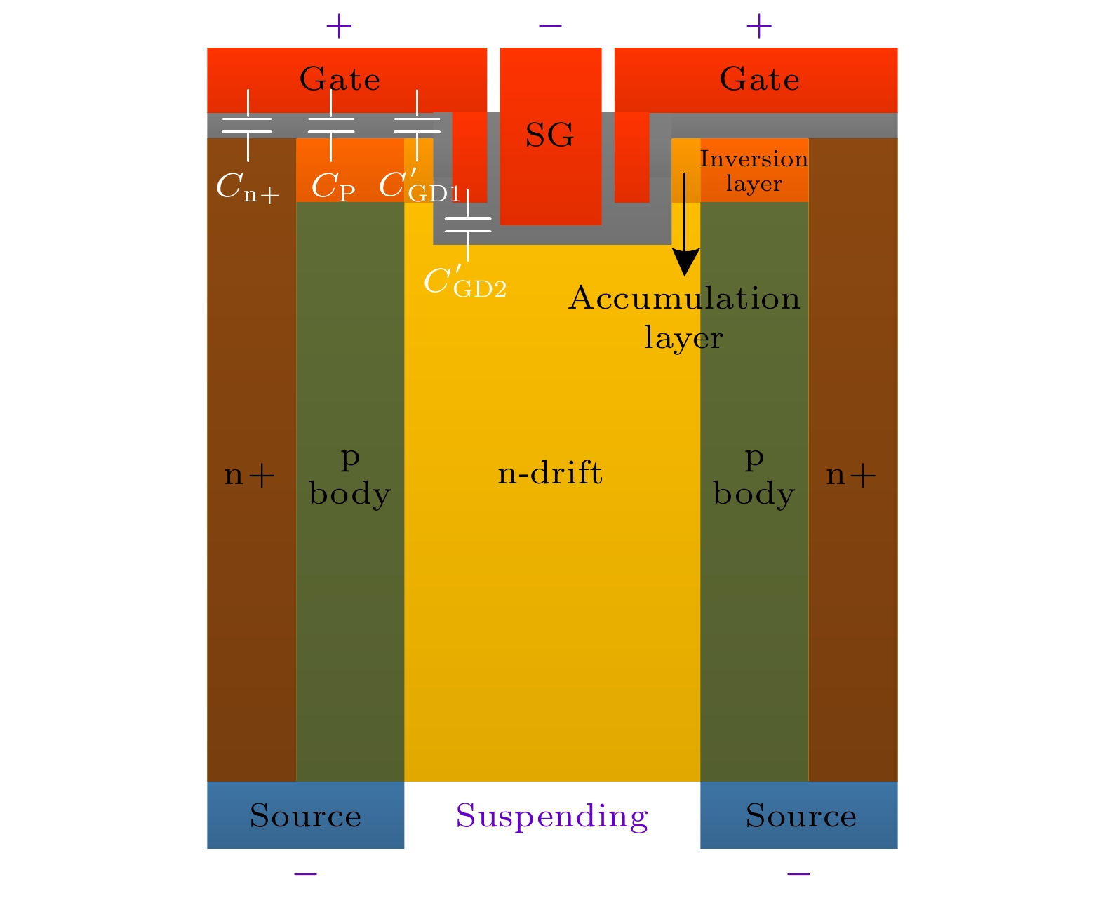
图 6 SGT-MOSFET正向耐压测试下简化后的栅极与元胞结构间的栅源电容CGS(+)组成示意图
Fig. 6. The simplified schematic diagram of SGT-MOSFET gate to source capacitor CGS(+) between the gate and the cell structure under forward pass voltage testing.
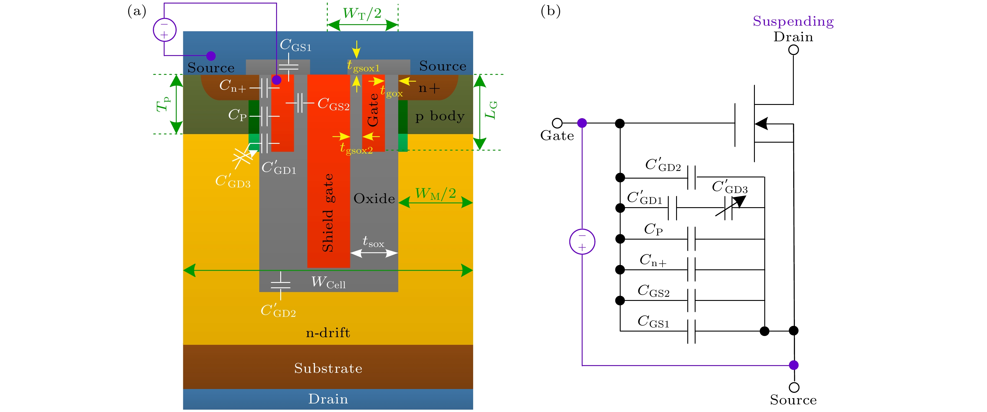
图 7 SGT-MOSET反向耐压测试下的栅源电容CGS(–) (a)及等效电路(b)示意图
Fig. 7. Schematic diagram of SGT-MOSET gate to source capacitor CGS(–) (a) and equivalent circuit (b) under reverse pass voltage testing.
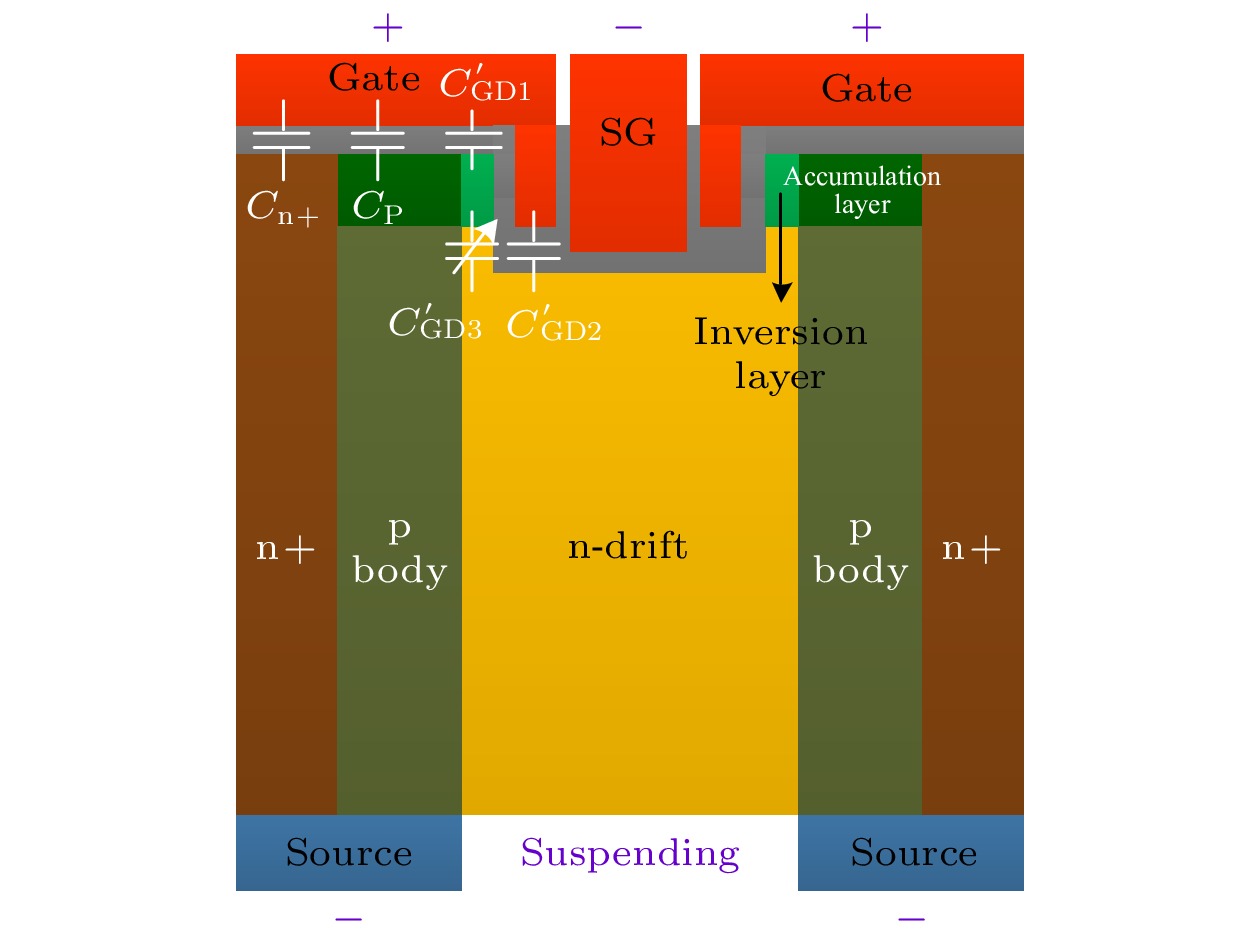
图 8 SGT-MOSFET反向耐压测试下简化后的栅极与元胞结构间的栅源电容CGS(–)组成示意图
Fig. 8. The simplified schematic diagram of SGT-MOSFET gate to source capacitor CGS(–) between the gate and the cell structure under reverse pass voltage testing.
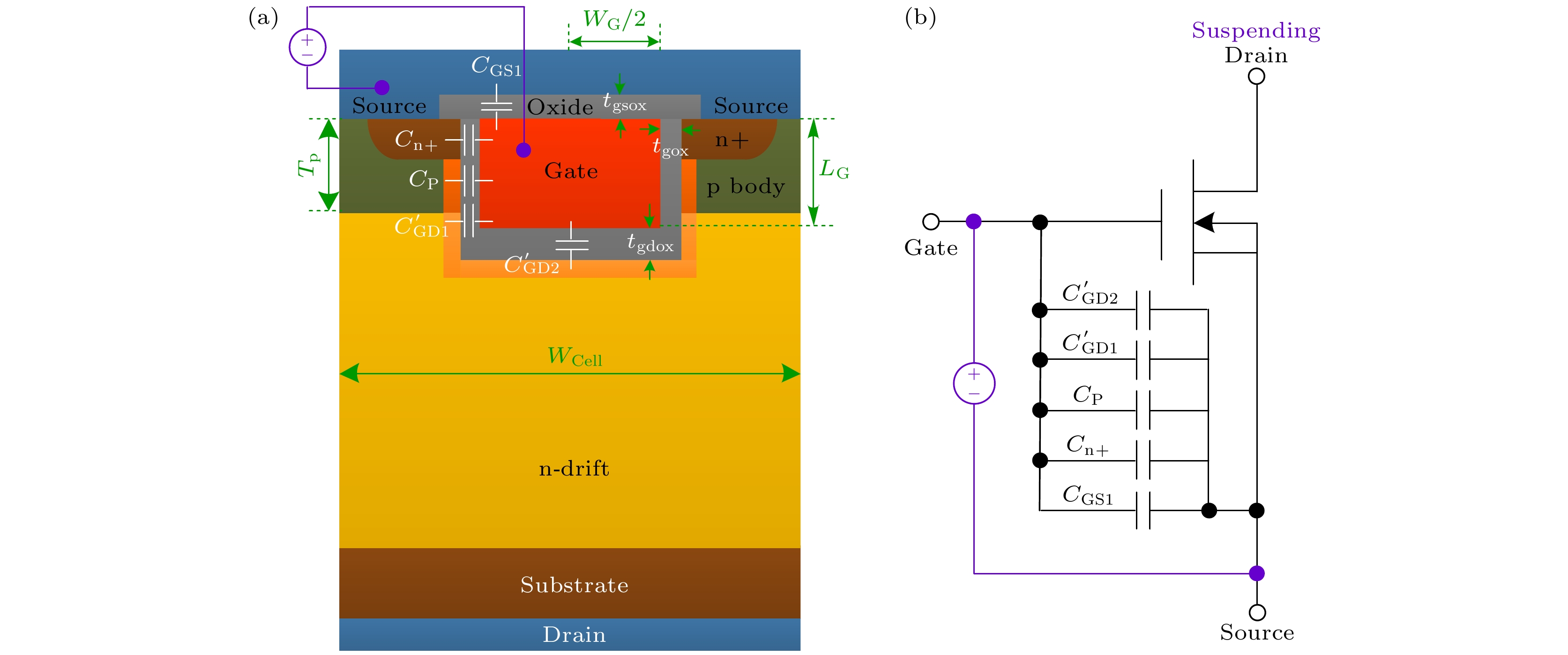
图 9 VUMOSFET正向耐压测试下的栅源电容CGS(+) (a)及等效电路(b)示意图
Fig. 9. Schematic diagram of VUMOSFET CGS(+) (a) and equivalent circuit (b) under forward pass voltage testing.
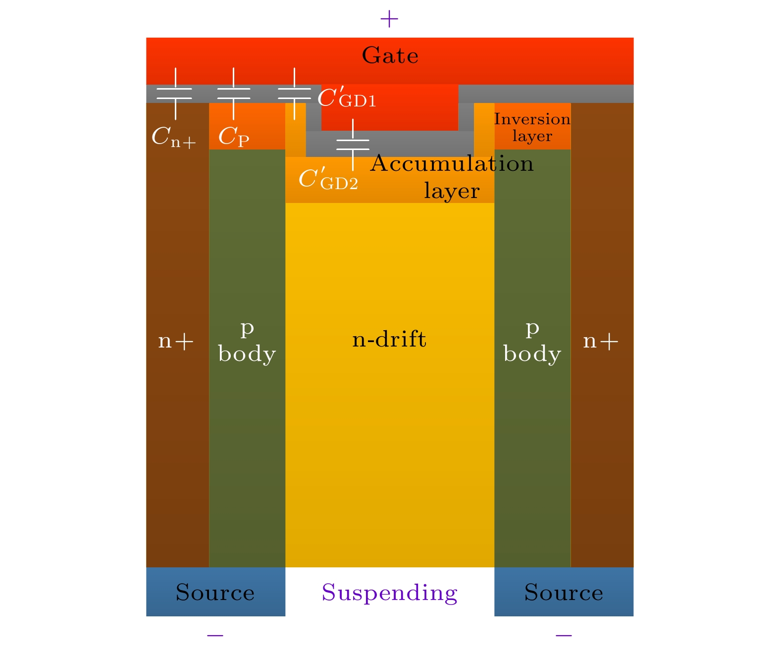
图 10 VUMOSFET正向耐压测试下简化后的栅极与元胞结构间的栅源电容CGS(+)组成示意图
Fig. 10. The simplified schematic diagram of VUMOSFET gate to source capacitor CGS(+) between the gate and the cell structure under forward pass voltage testing.
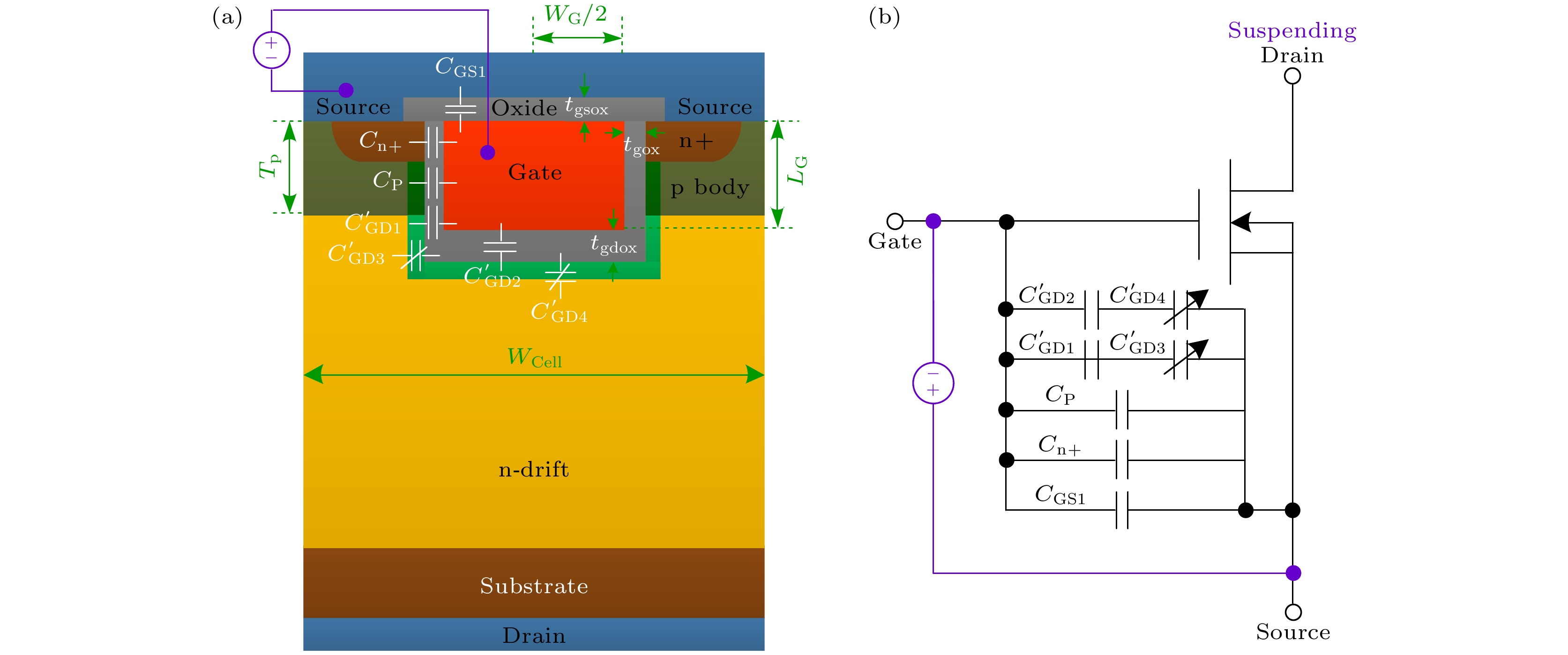
图 11 VUMOSET反向耐压测试下的栅源电容CGS(–) (a)及等效电路(b)示意图
Fig. 11. Schematic diagram of VUMOSET gate to source capacitor CGS(–) (a) and equivalent circuit (b) under reverse pass voltage testing.
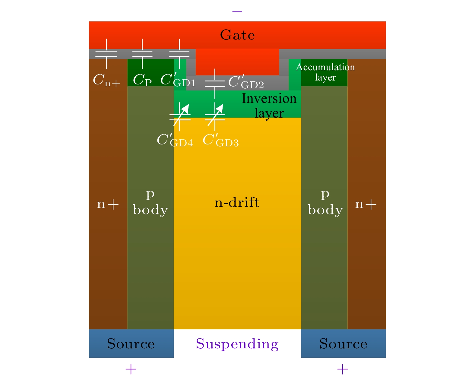
图 12 VUMOSET反向耐压测试下简化后的栅极与元胞结构间的栅源电容CGS(–)组成示意图
Fig. 12. The simplified schematic diagram of VUMOSET gate to source capacitor CGS(–) between the gate and the cell structure under reverse pass voltage testing.
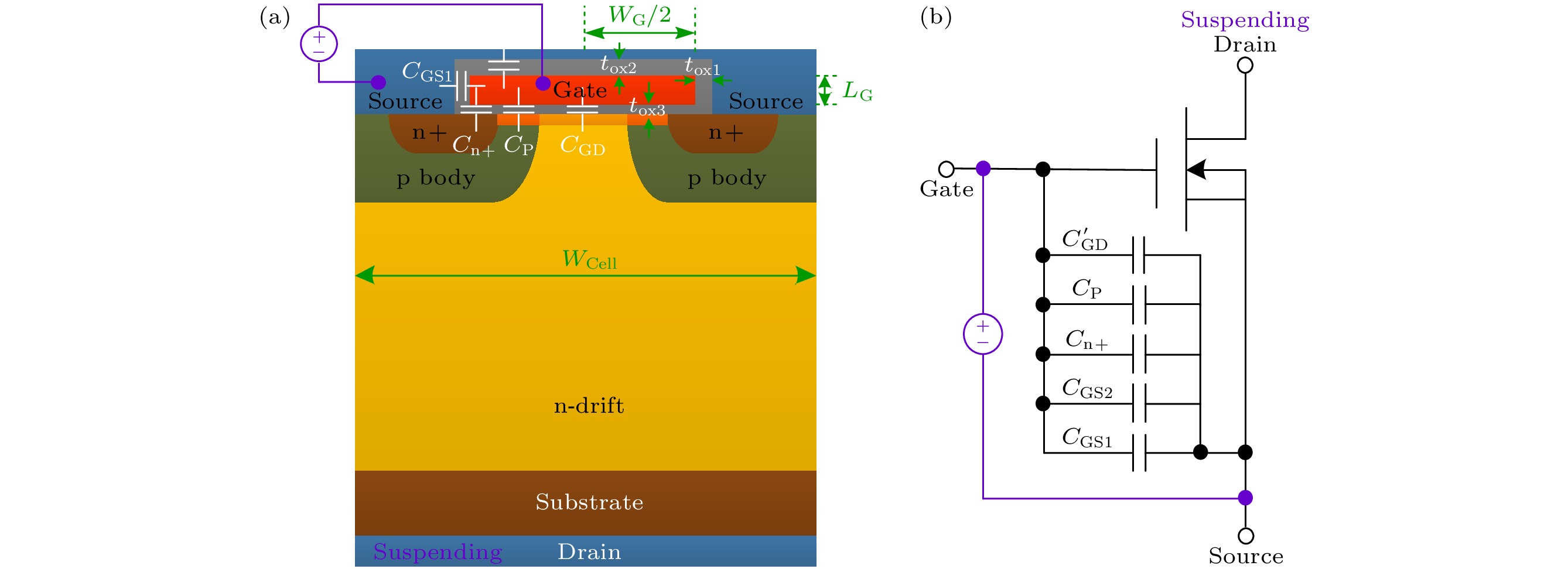
图 13 VDMOS正向耐压测试下的栅源电容CGS(+) (a)及等效电路(b)示意图
Fig. 13. Schematic diagram of VDMOS gate to source capacitor CGS(+)(a) and equivalent circuit (b).
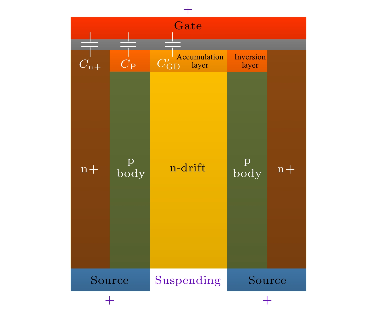
图 14 VDMOS正向耐压测试下简化后的栅极与元胞结构间的栅源电容CGS(+)组成示意图
Fig. 14. The simplified schematic diagram of VDMOS gate to source capacitor CGS(+) between the gate and the cell structure under forward pass voltage testing.
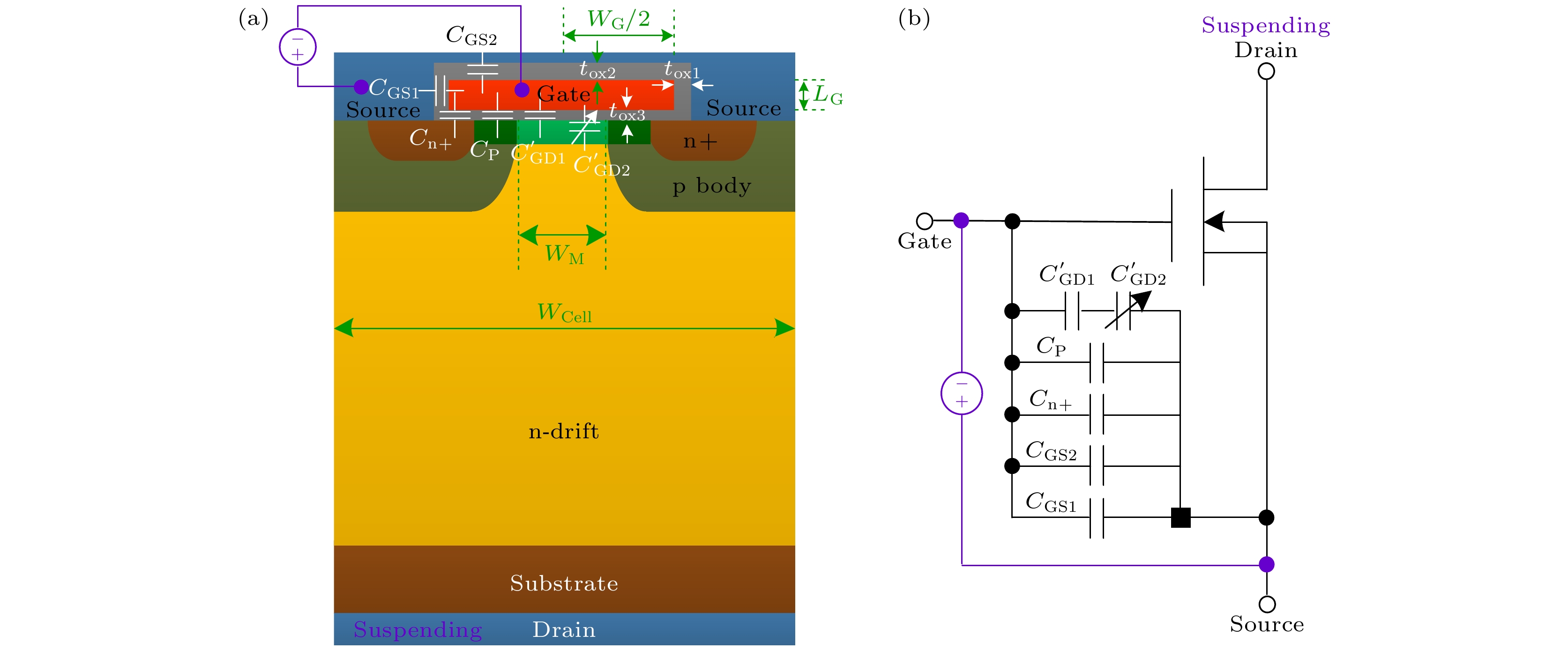
图 15 VDMOS反向耐压测试下的栅源电容CGS(–) (a)及等效电路(b)示意图
Fig. 15. Schematic diagram of VDMOS gate to source capacitor CGS(–) (a) and equivalent circuit (b) under reverse pass voltage testing
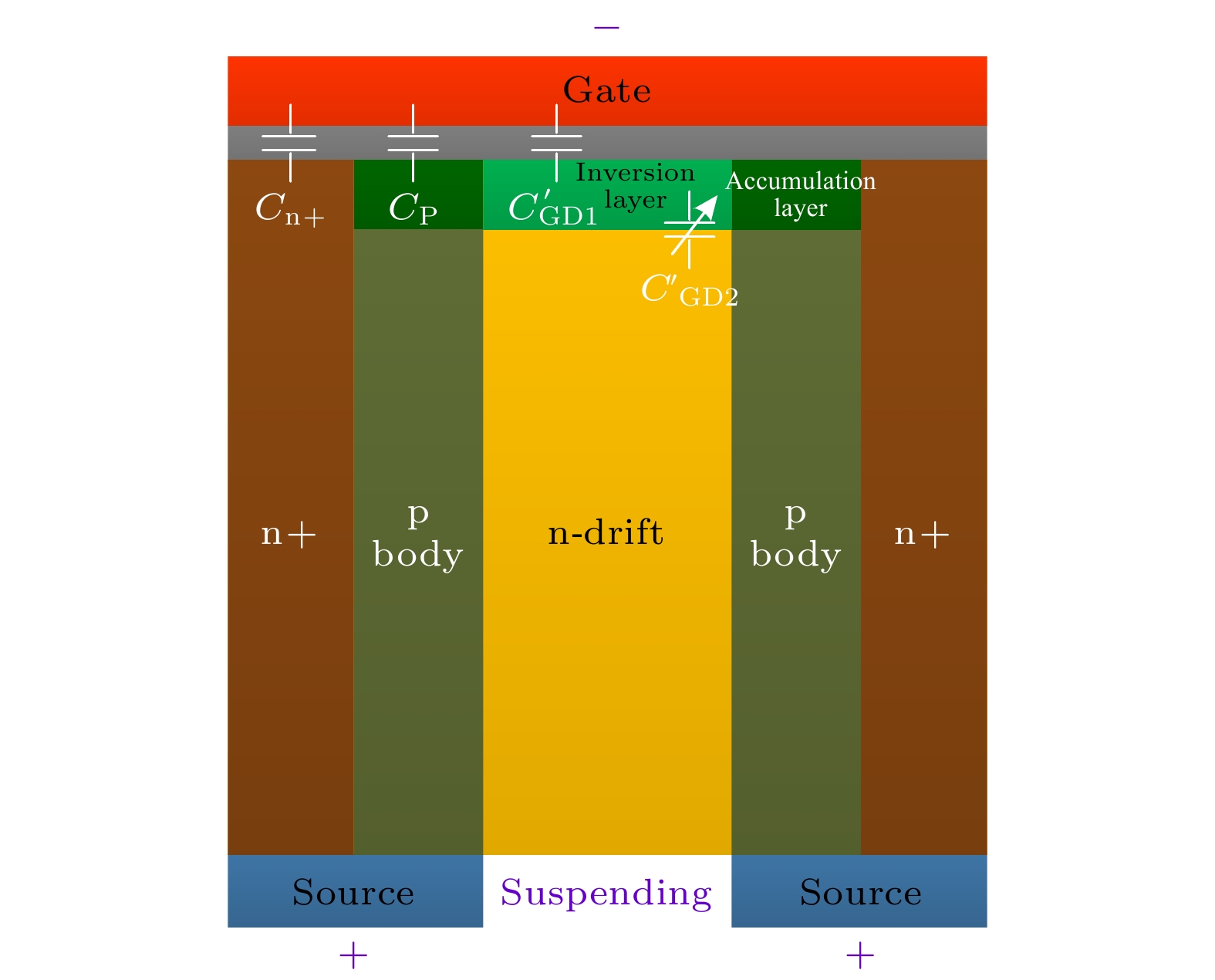
图 16 VDMOS反向耐压测试下简化后的栅极与元胞结构间的栅源电容CGS(–)组成示意图
Fig. 16. The simplified schematic diagram of VDMOS gate to source capacitor CGS(–) between the gate and the cell structure under reverse pass voltage testing.
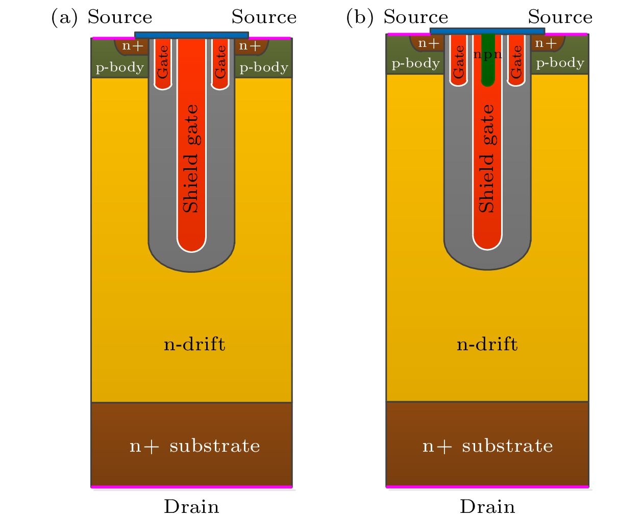
图 17 SGT-MOSFET改进结构 (a) 传统结构; (b) NPN-SG结构
Fig. 17. The improved structure of SGT-MOSFET: (a) Traditional structures; (b) NPN-SG structures.
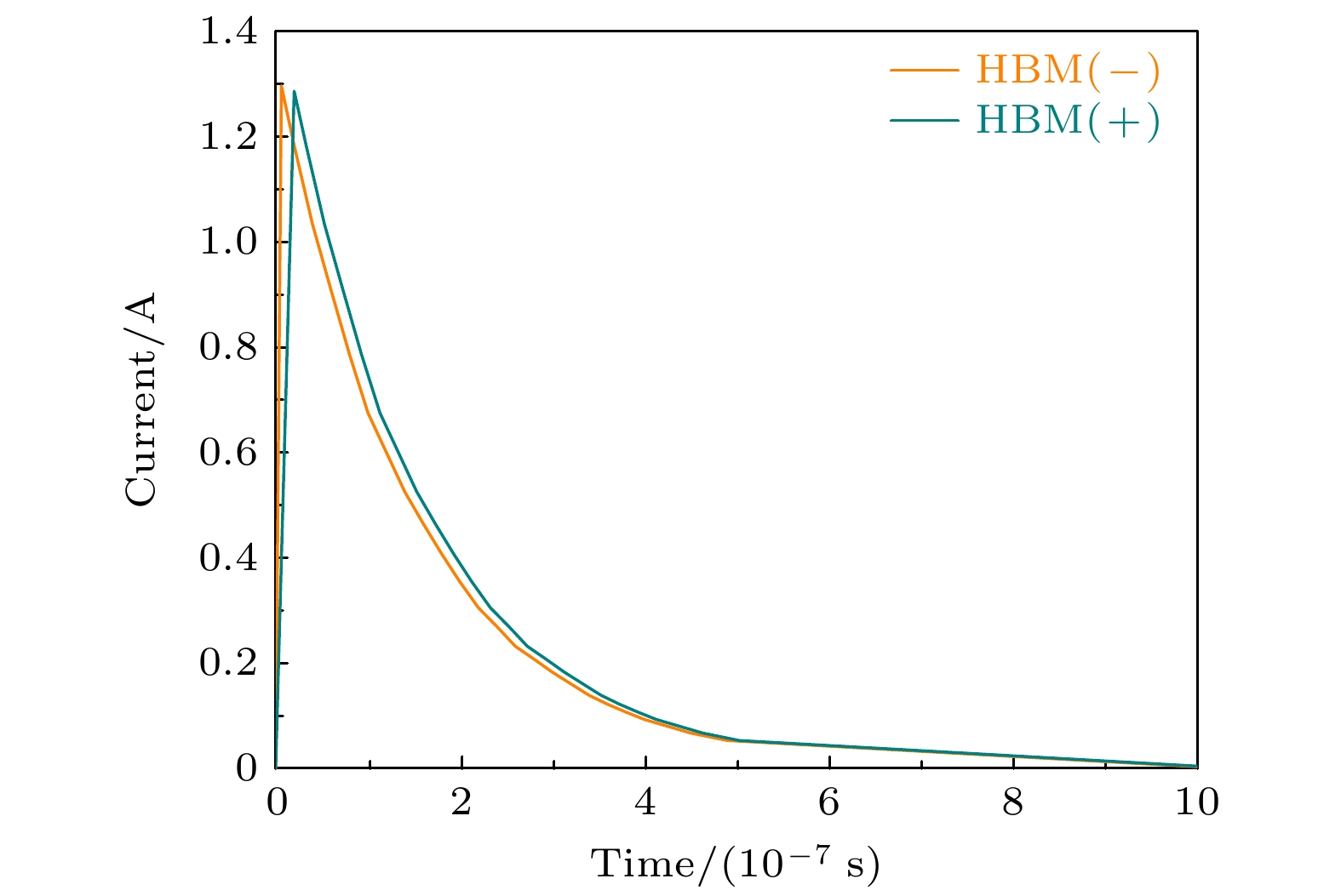
图 18 NPN-SG结构在HBM下的放电波形
Fig. 18. The discharge waveform of NPN-SG structures under HBM
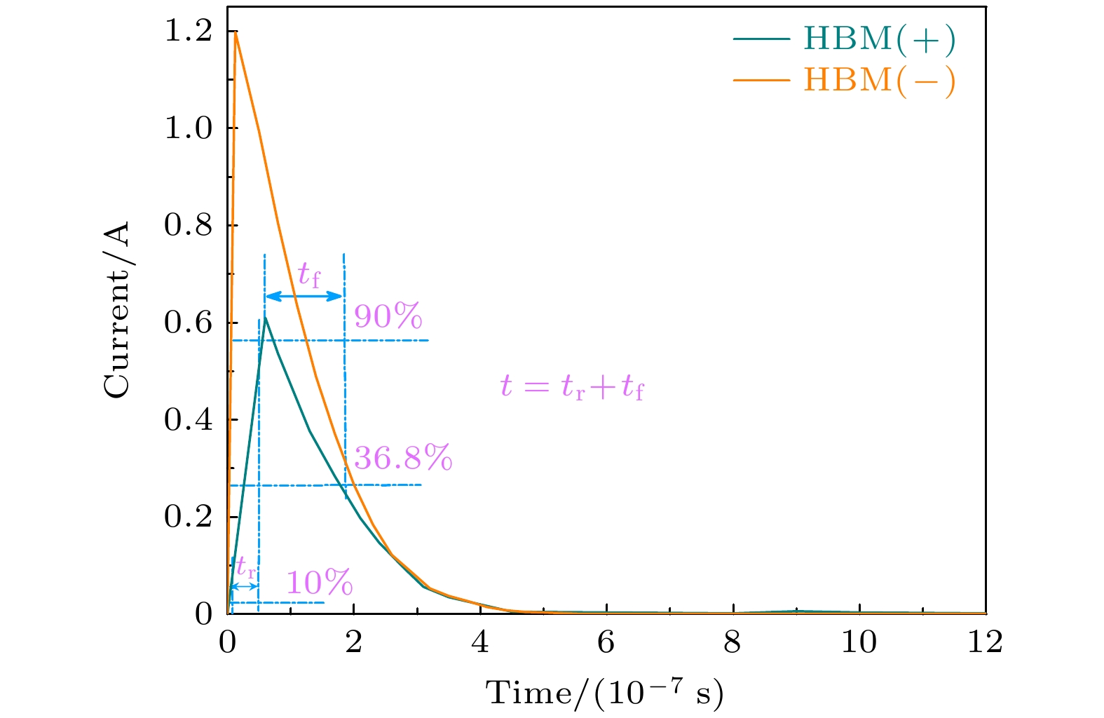
图 19 VDMOS在HBM模型下的放电波形 (RHBM1 = 1 MΩ, RHBM2 = 1500Ω, RHBM3 = 500Ω, CHBM = 100 pF)
Fig. 19. The discharge waveform of VDMOS under the HBM model (RHBM1 = 1 MΩ, RHBM2 = 1500Ω, RHBM3 = 500Ω, CHBM = 100 pF)
表 1 SGT-MOSFET, VUMOSFET, VDMOS不同型号产品HBM测试的正反向耐压数据
Table 1. Positive and reverse withstand voltage data for HBM tests of VDMOS, VUMOSFET, SGT-MOSFET.
器件类型 样品型号 ESD正向
耐压/VESD反向
耐压/VSGT-MOSFET SW036R10E8S 600 1010 SW050R10E8S 750 1450 SW050R85E8S 670 1390 SW050R95E8S 810 1590 SW083R06VLS 480 830 VUMOSFET SW065R68E7T 520 1640 SW067R68E7T 650 2350 SW068R68E7T 680 1970 SW065R03VLT 450 1360 SW018R03VLT 830 2800 VDMOS SW7N60D 1350 3140 SW10N60D 1470 3520 SW12N65D 1530 3690 SW20N65D 1560 3510 SW7N80D 1670 3940  下载: 导出CSV
表 2 SGT-MOSFET, VUMOSFET, VDMOS不同型号产品的相关参数
Table 2. Related parameters of different products of VDMOS, VUMOSFET, SGT-MOSFET.
器件类型 样品型号 封装形式 击穿电压/V 阈值电压/V 导通电阻/mΩ SGT-MOSFET SW036R10E8S TO-220 100 3 3.8 SW050R10E8S TO-220 100 3 5.7 SW050R85E8S TO-263 85 3 5.2 SW050R95E8S TO-263 95 3 5.9 SW083R06VLS TO-251 60 2 9.6 VUMOSFET SW065R68E7T TO-220 68 3 6.3 SW067R68E7T TO-220 68 3 6.9 SW068R68E7T TO-252 68 3 7.0 SW065R03VLT TO-252 30 3 6.6 SW018R03VLT DFN5*6 30 1.8 1.6 VDMOS SW7N60D TO-220 600 3.5 1.1 SW10N60D TO-220F 600 3.5 0.9 SW12N65D TO-220F 650 3.5 0.6 SW20N65D TO-220F 650 3.7 0.3 SW7N80D TO-220F 800 3.5 1.5
下载: 导出CSV
-
[1] Jung D Y, Park K S, Kim S I, Kwon S, Cho D H, Jang H G, Lim J W 2023 ETRI J. 45 543
Google Scholar
[2] Mai X C, Chen S L, Chen H W, Lee Y M 2023 Electronics 12 2803
Google Scholar
[3] Yan Y, Lan W, Chen Y, Yang D, Zhou Y, Zhu Z, Liou J J 2022 Adv. Electron. Mater. 8 2100886
[4] Anderson N T, Lockledge S P 2022 ASM International Pasadena, USA, October 30–November 3, 2022 pp329–332
[5] Smallwood J M 2023 J. Electrostat. 125 103817
Google Scholar
[6] Ker M D, Pommerenke D 2022 IEEE Trans. on Electromagn. Compat. 64 1783
Google Scholar
[7] Yang L, Yang C, Tu Y, Wang X, Wang Q 2021 IEEE Access 9 33512
Google Scholar
[8] Ji Q, Luo A, Liu Q, Wan B 2023 International Conference on Optoelectronic Information and Functional Materials 2023 12781
[9] Gimenez S P, Galembeck E H S 2023 ECS Trans. 111 161
Google Scholar
[10] Ajay 2021 Silicon 13 1325
Google Scholar
[11] Hong S Z, Chen S L, Chen H W, Lee Y M 2021 IEEE Electron Device Lett. 42 1512
Google Scholar
[12] Lai J Y, Chen S L, Liu Z W, Chen H W, Chen H H, Lee Y M 2022 Sens. Mater. 34 1835
[13] Zhu Z, Yang Z, Fan X, W Fan 2021 Crystals 11 128
Google Scholar
[14] Luo X, Xu J, Xu X, Luo H, Dai Z 2022 2022 International EOS/ESD Symposium on Design and System Chengdu China, November 9–11, 2022 p2023-03-22
[15] Arosio M, Boffino C, Morini S, Dirk Priefert, Oezguer Albayrak, Viktor Boguszewicz, Andrea Baschirotto 2021 IEEE Trans Electron. Devices 68 2848
Google Scholar
[16] 苏乐, 王彩琳, 杨武华, 梁晓刚, 张超 2023 物理学报 72 148501
Google Scholar
Su L, Wang C L, Yang W H, Liang X G, Zhang C 2023 Acta Phys. Sin. 72 148501
Google Scholar
[17] Xi J, Wang J, Lu J, Chen J, Xin Y, Li Z, Tu C, Shen Z J 2018 Microelectron. Reliab. 88-90 593
Google Scholar
[18] Su L, Wang C L, Yang W H, Zhang C 2023 Microelectron. Reliab. 143 114950
Google Scholar
[19] Tian Y, Yang Z, Xu Z, Liu S, Sun W F, Shi L, Zhu Y, Ye P, Zhou J 2018 Superlattices Microstruct. 116 151
Google Scholar
[20] Su L, Wang C L, Yang W H, An J 2022 Microelectron. Reliab. 139 114822
Google Scholar
[21] Sun J, Zheng Z, Zhang L, Chen K J 2022 2022 IEEE 34th International Symposium on Power Semiconductor Devices and ICS Vancouver, Canada, May 22–25, 2022 pp73–76

 下载:
下载:
计量
- 文章访问数: 5118
- PDF下载量: 103
- 被引次数: 0
