


-
设计了一种由椭圆介电柱子组成的正方晶格光子晶体结构. 通过调节椭圆柱子的大小和放置角度, 在布里渊区中心同时实现两个不同频率的双重偶然简并, 并获得两个不同波段的半狄拉克锥. 更有趣的是, 这两个半狄拉克锥沿椭圆柱子长轴和短轴两个方向表现出的线性和非线性色散关系正好相反,
${\boldsymbol{k}} \cdot {\boldsymbol{p}}$ 微扰理论也进一步证实了这种奇异的色散关系. 数值计算结果表明在两个半狄拉克点频率附近, 本文所设计的正方晶格光子晶体在线性色散所在方向上等效为阻抗匹配的双零折射率材料, 而在非线性色散所在方向上只能等效为单零折射率材料, 即沿椭圆柱子长轴和短轴两个方向的等效零折射率展现出差异性. 而两个不同波段的半狄拉克锥所对应的这种等效零折射率的各向异性截然相反, 因此可利用“Y”型光子晶体板将两种不同频率的电磁波成功分离.Semi-Dirac cones, a type of unique dispersion relation, always exhibit a series of interesting transport properties, such as electromagnetic topological transitions and anisotropic electromagnetic transmission. Recently, dual-band semi-Dirac cones have been found in three-dimensional photonic crystals, presenting great potential in electromagnetic wave regulation. However, to the best of our knowledge, there has been no report on dual-band semi-Dirac cones and their applications in two-dimensional photonic crystals, and most of two-dimensional systems have only realized semi-Dirac cones at a single frequency. Therefore, we are to realize dual-band semi-Dirac cones in two-dimensional photonic crystals. In this work, a type of two-dimensional photonic crystal that comprises a square lattice of elliptical cylinders embedded in air is proposed. By rotating the elliptical cylinders and adjusting their sizes appropriately, accidental degeneracy at two different frequencies is achieved simultaneously in the center of the Brillouin zone. Using ${\boldsymbol{k}} \cdot {\boldsymbol{p}}$ perturbation theory, the dispersion relations near the two degenerate points are proved to be nonlinear in one direction, and linear in other directions. These results indicate that the double accidental degenerate points are two semi-Dirac points with different frequencies, and two different semi-Dirac cones, i.e. dual-band semi-Dirac cones, are realized simultaneously in our designed photonic crystal. More interestingly, the dual-band semi-Dirac cones exhibit opposite linear and nonlinear dispersion relation along the major axis and the minor axis of the ellipse, respectively. And our photonic crystal can be equivalent to an impedance-matched double-zero index material in the direction of linear dispersion and a single-zero index material in the direction of nonlinear dispersion, which is demonstrated by the perfect transmission in the straight waveguide and wavefront shaping capabilities of electromagnetic waves. Based on the different properties of the equivalent zero-refractive-indices near the frequencies of two semi-Dirac point, the designed Y-type waveguide can be used to realize frequency separation by leading out the plane waves of different frequencies along different ports. We believe that our work is meaningful in broadening the exploration of the band structures of two-dimensional photonic crystals and providing greater convenience for regulating electromagnetic waves.
-
Keywords:
- photonic crystal /
- semi-Dirac cone /
- zero-index material
[1] Castro Neto A H, Guinea F, Peres N M R, Novoselov K S, Geim A K 2009 Rev. Mod. Phys. 81 109
 Google Scholar
[2] Geim A K, Novoselov K S 2007 Nat. Mater. 6 183
Google Scholar
[3] Zandbergen S R, de Dood M J A 2010 Phys. Rev. Lett. 104 043903
Google Scholar
[4] Zhang X D, Liu Z Y 2008 Phys. Rev. Lett. 101 264303
Google Scholar
[5] Zhang X D 2008 Phys. Rev. Lett. 100 113903
Google Scholar
[6] Li Y, Wu Y, Chen X, Mei J 2013 Opt. Express 21 7699
Google Scholar
[7] Mei J, Wu Y, Chan C T, Zhang Z Q 2012 Phys. Rev. B 86 035141
Google Scholar
[8] Luo J, Lai Y 2022 Front. Phys. 10 845624
Google Scholar
[9] 周晓霞, 陈英, 蔡力 2023 物理学报 72 174205
Google Scholar
Zhou X X, Chen Y, Cai L 2023 Acta Phys. Sin. 72 174205
Google Scholar
[10] Huang X Q, Lai Y, Hang Z H, Zheng H H, Chan C T 2011 Nat. Mater. 10 582
Google Scholar
[11] Xu C Q, Lyu K Q, Wu Y 2023 EPL 141 15002
Google Scholar
[12] Wang X, Jiang H T, Yan C, Deng F S, Sun Y, Li Y H, Shi Y L, Chen H 2014 EPL 108 14002
Google Scholar
[13] 黄学勤, 陈子亭 2015 物理学报 64 184208
Google Scholar
Huang X Q, Chan C T 2015 Acta Phys. Sin. 64 184208
Google Scholar
[14] Dong J W, Chang M L, Huang X Q, Hang Z H, Zhong Z C, Chen W J, Huang Z Y, Chan C T 2015 Phys. Rev. Lett. 114 163901
Google Scholar
[15] Li Y, Chan C T, Mazur E 2021 Light Sci. Appl. 10 203
Google Scholar
[16] Sakoda K 2012 Opt. Express 20 9925
Google Scholar
[17] Li Y, Mei J 2015 Opt. Express 23 12089
Google Scholar
[18] Wu Y 2014 Opt. Express 22 1906
Google Scholar
[19] 曹惠娴, 梅军 2015 物理学报 64 194301
Google Scholar
Cao H X, Mei J 2015 Acta Phys. Sin. 64 194301
Google Scholar
[20] Yasa U G, Turduev M, Giden I H, Kurt H 2018 Phys. Rev. B 97 195131
Google Scholar
[21] Zhang X J, Wu Y 2015 Sci. Rep. 5 7892
Google Scholar
[22] Yang Y T, Jia Z Y, Xu T, Luo J, Lai Y, Hang Z H 2019 Appl. Phys. Lett. 114 161905
Google Scholar
[23] Bor E, Turduev M, Yasa U G, Kurt H, Staliunas K 2018 Phys. Rev. B 98 245112
Google Scholar
[24] Yan Y, Luo Y J 2023 Opt. Laser Technol. 164 109558
Google Scholar
[25] He X T, Zhong Y N, Zhou Y, Zhong Z C, Dong J W 2015 Sci. Rep. 5 13085
Google Scholar
[26] Vertchenko L, DeVault C, Malureanu R, Mazur E, Lavrinenko A 2021 Laser Photonics Rev. 15 2000559
Google Scholar
[27] Bor E, Yasa U G, Kurt H, Turduev M 2020 Opt. Lett. 45 2423
Google Scholar
[28] Li M Y, Mei R, Yan D Y, Ma Z K, Cao F, Xu Y D, Xu C Q, Luo J 2024 Phys. Rev. B 109 125432
Google Scholar
[29] Goerbig M O 2011 Rev. Mod. Phys. 83 1193
Google Scholar
[30] Pardo V, Pickett W E 2009 Phys. Rev. Lett. 102 166803
Google Scholar
[31] Banerjee S, Singh R R P, Pardo V, Pickett W E 2009 Phys. Rev. Lett. 103 016402
Google Scholar
[32] Montambaux G, Piéchon F, Fuchs J N, Goerbig M O 2009 Phys. Rev. B 80 153412
Google Scholar
[33] Xiang H X, Zhai F 2024 Phys. Rev. B 109 035432
Google Scholar
[34] Ye P P, Xu L, Zhang J 2018 Mod. Phys. Lett. B 32 1850193
Google Scholar
[35] Assili M, Haddad S 2013 J. Phys. Condens. Matter 25 365503
Google Scholar
-
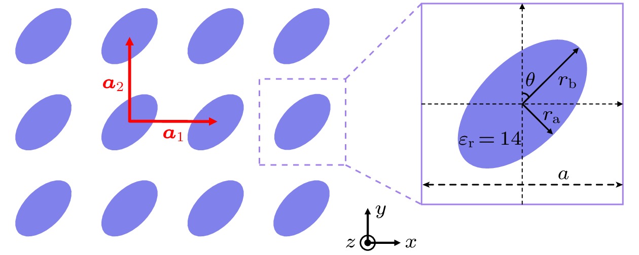
图 1 正方晶格光子晶体结构及其原胞示意图
Fig. 1. Schematic diagram of a square-lattice photonic crystal and its unit cell.
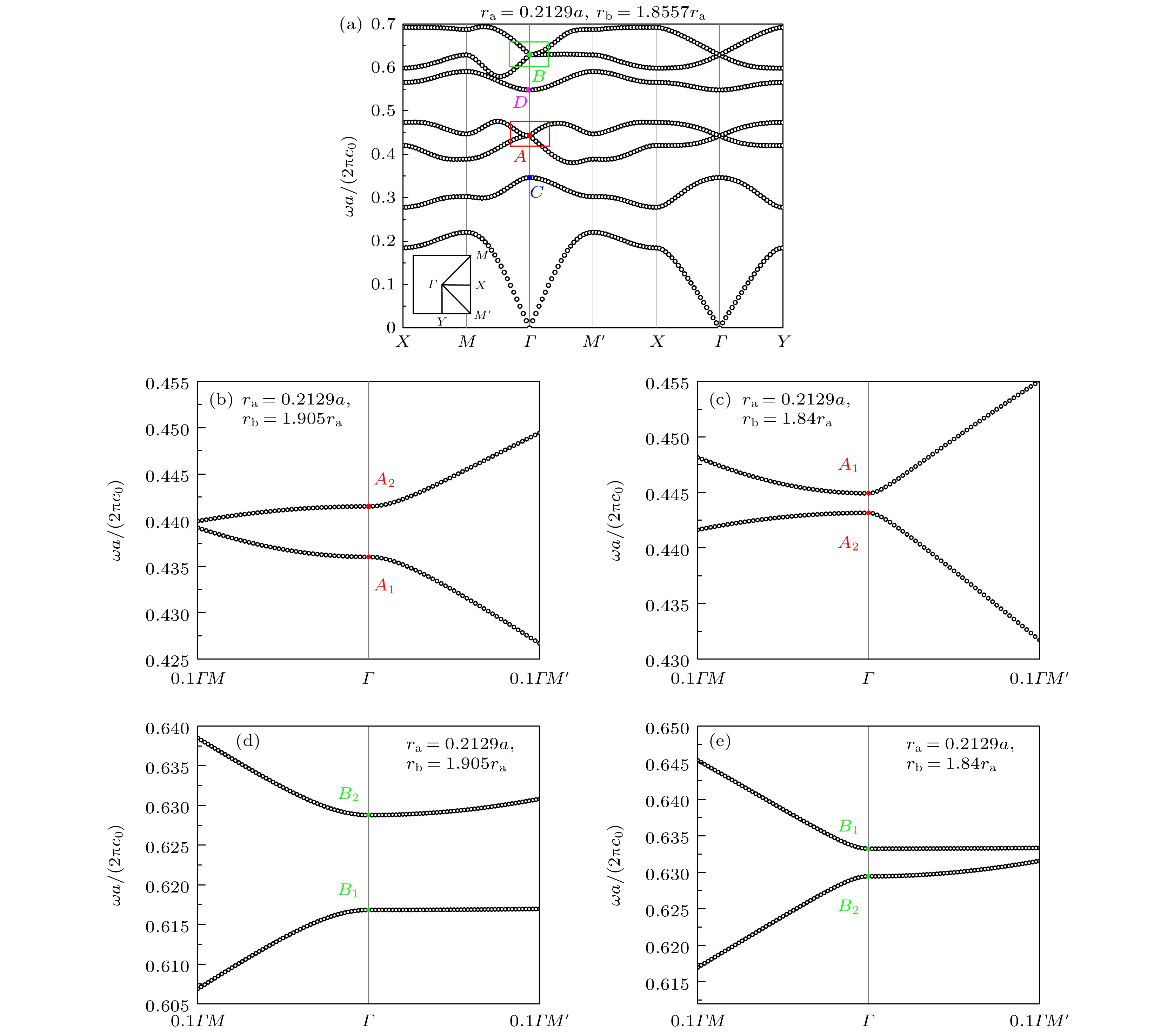
图 2 (a) $ \theta = {45^ \circ } $时光子晶体的能带结构, 左下角插图为第一布里渊区; (b) 椭圆长轴增大后打开A点简并所对应的能带结构放大图; (c) 椭圆长轴缩短后打开A点简并所对应的能带结构放大图; (d) 椭圆长轴增大后打开B点简并所对应的能带结构放大图; (e) 椭圆长轴缩短后打开B点简并所对应的能带结构放大图
Fig. 2. (a) Band structure of the photonic crystal when $ \theta = {45^ \circ } $, where the inset in the lower left corner shows the first Brillouin zone; (b) enlarged view of the band structure after enlarging the major axis of the ellipse and opening the degeneracy of point A; (c) enlarged view of the band structure after shortening the major axis of the ellipse and opening the degeneracy of point A; (d) enlarged view of the band structure after enlarging the major axis of the ellipse and opening the degeneracy of point B; (e) enlarged view of the band structure after shortening the major axis of the ellipse and opening the degeneracy of point B.
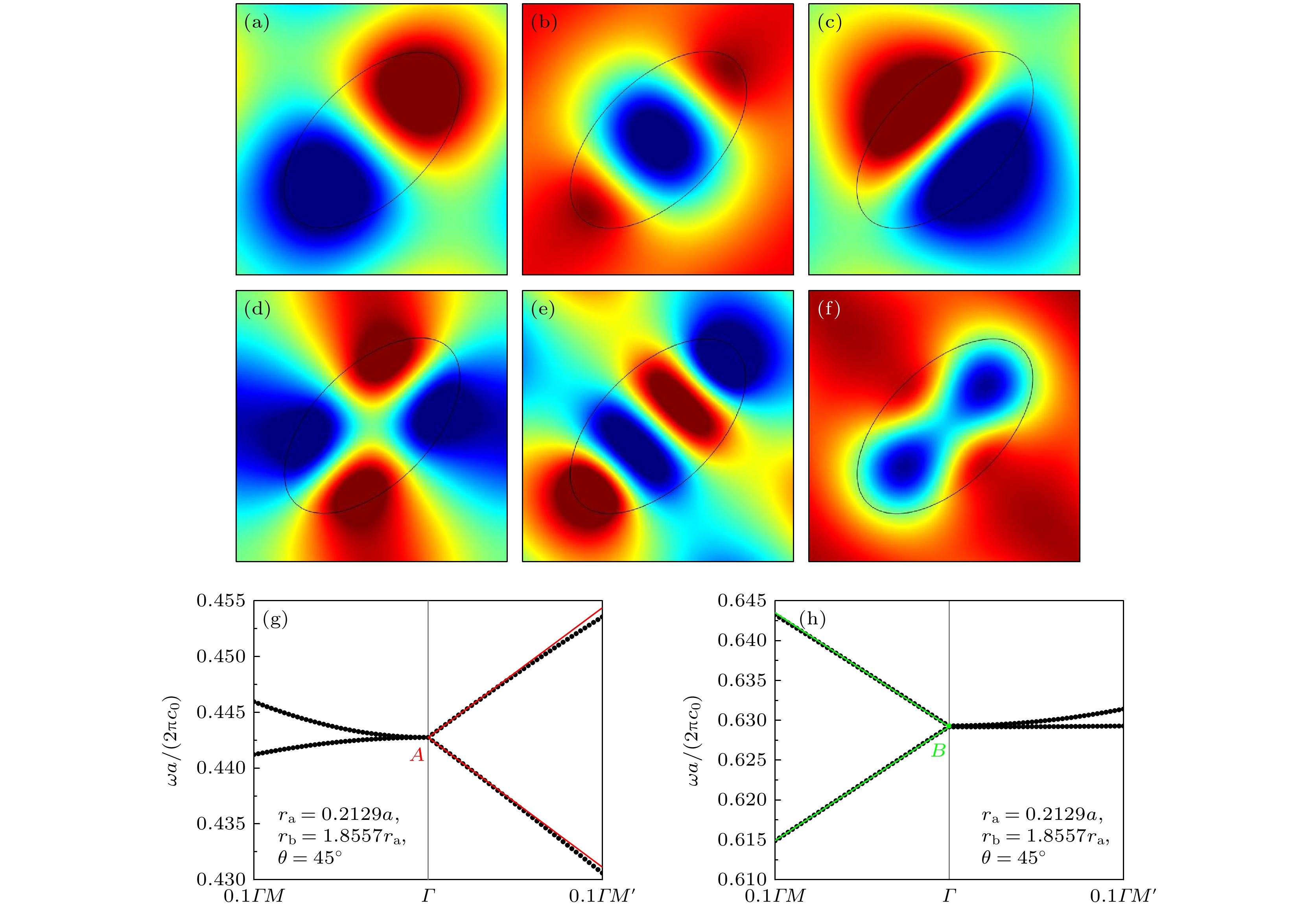
图 3 (a) C点偶极子态的电场分布图; (b) A点单极子态的电场分布图; (c) A点偶极子态的电场分布图; (d) D点四极态的电场分布图; (e) B点其中一个简并态的电场分布图; (f) B点另一个简并态的电场分布图; (g) 半狄拉克点A附近能带放大图; (h) 半狄拉克点B附近能带放大图
Fig. 3. (a) Electric field pattern at point C, which indicates a dipolar state; (b) the electric field pattern at point A, which indicates a monopolar state; (c) the electric field pattern at point A, which indicates a dipolar state; (d) the electric field pattern at point D, which indicates a quadrupolar state; (e) the electric field pattern of one of the degenerate states at point B; (f) the electric field pattern of the other degenerate state at point B; (g) an enlarged view of the band structure near the semi-Dirac point A; (h) an enlarged view of the band structure near the semi-Dirac point B.
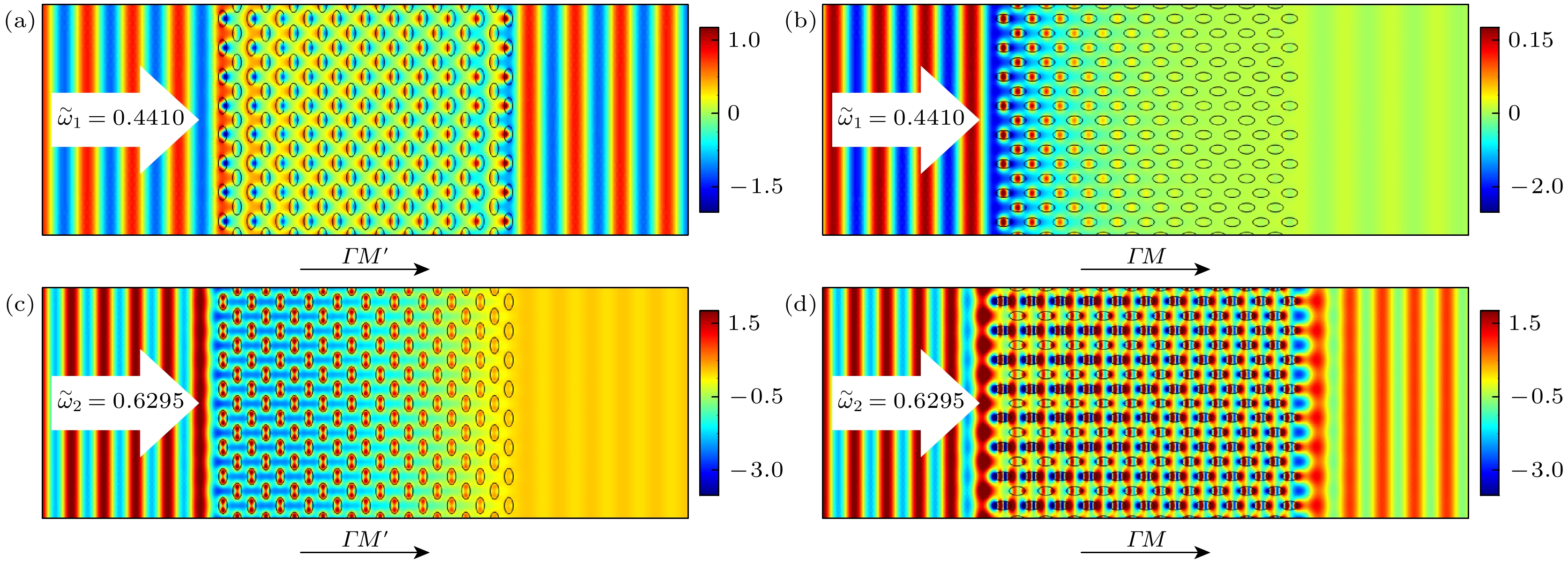
图 4 (a) 频率${\tilde \omega _1} = 0.4410$的平面波沿$\varGamma M'$方向入射时的电场分布; (b) 频率${\tilde \omega _1} = 0.4410$的平面波沿$\varGamma M$方向入射时的电场分布; (c) 频率${\tilde \omega _2} = 0.6295$的平面波沿$\varGamma M'$方向入射时的电场分布; (d) 频率${\tilde \omega _2} = 0.6295$的平面波沿$\varGamma M$方向入射时的电场分布
Fig. 4. (a) Electric field pattern when a plane wave with a frequency of $ {\tilde \omega _1} = 0.4410 $ is transmitted along the $\varGamma M'$ direction; (b) the electric field pattern when a plane wave with a frequency of $ {\tilde \omega _1} = 0.4410 $ is transmitted along the $\varGamma M$ direction; (c) the electric field pattern when a plane wave with a frequency of $ {\tilde \omega _2} = 0.6295 $ is transmitted along the $ \varGamma M' $ direction; (d) the electric field pattern when a plane wave with a frequency of $ {\tilde \omega _2} = 0.6295 $ is transmitted along the $\varGamma M$ direction.
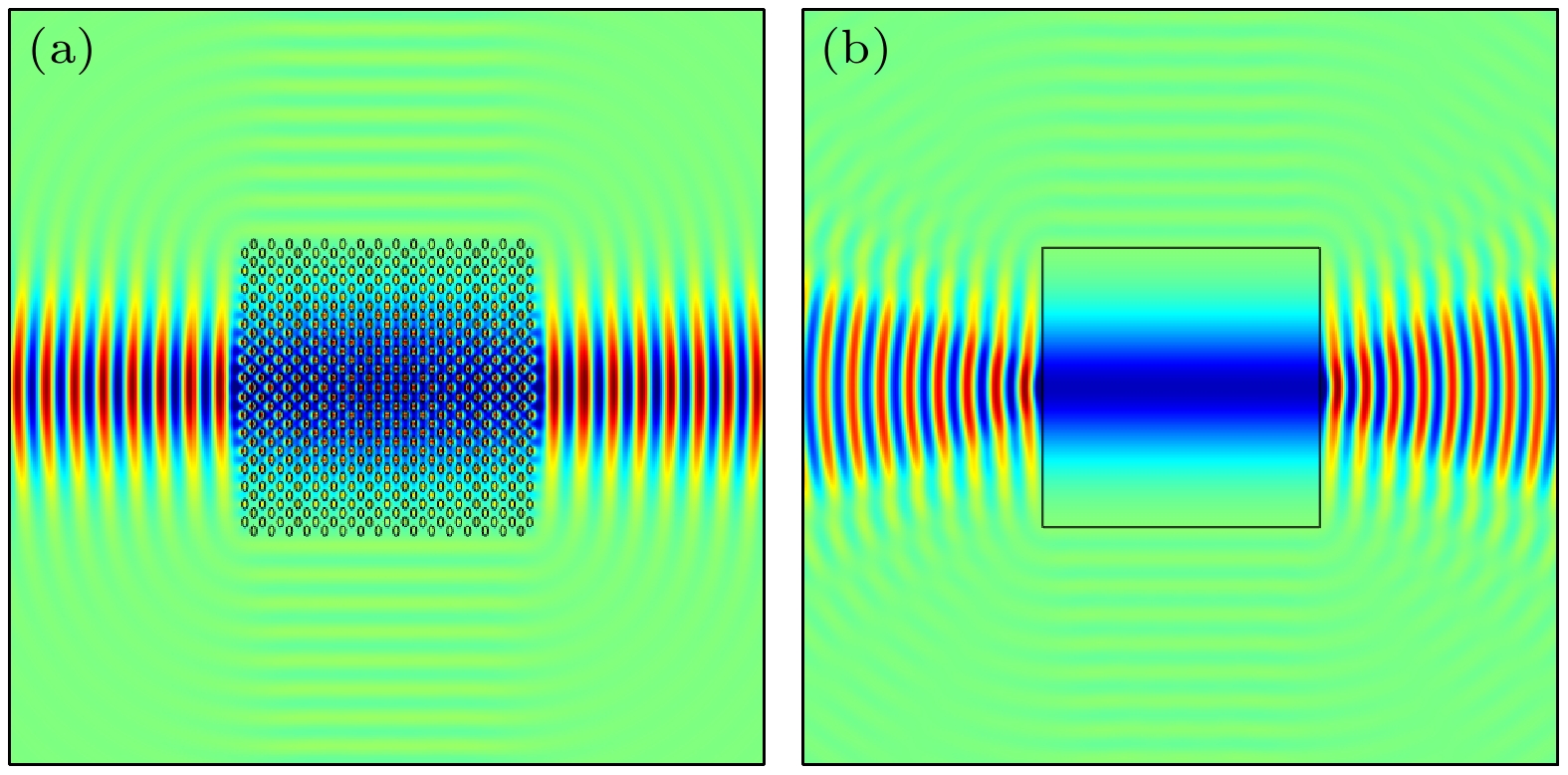
图 5 (a) 频率${\tilde \omega _1} = 0.4410$的点源放置在$ 16 \times 16 $的光子晶体阵列中的电场分布; (b) 频率${\tilde \omega _1} = 0.4410$的点源放置在均匀各向异性零折射率材料中的电场分布
Fig. 5. (a) Electric field pattern when a point source with a frequency of $ {\tilde \omega _1} = 0.4410 $ is placed inside the center of a $ 16 \times 16 $ dielectric photonic crystal array; (b) the electric field pattern when a point source with a frequency of $ {\tilde \omega _1} = 0.4410 $ is placed inside the center of a homogeneous anisotropic zero-index material.

图 6 (a) 频率${\tilde \omega _1} = 0.4410$的平面波在“Y”型波导中传输的电场分布; (b) 频率${\tilde \omega _3} = 0.6320$的平面波在“Y”型波导中传输的电场分布
Fig. 6. (a) Electric field pattern of a plane wave with a frequency of $ {\tilde \omega _1} = 0.4410 $ propagating in a Y-type waveguide; (b) the electric field pattern of a plane wave with a frequency of ${\tilde \omega _3} = 0.6320$ propagating in a Y-type waveguide.
-
[1] Castro Neto A H, Guinea F, Peres N M R, Novoselov K S, Geim A K 2009 Rev. Mod. Phys. 81 109
Google Scholar
[2] Geim A K, Novoselov K S 2007 Nat. Mater. 6 183
Google Scholar
[3] Zandbergen S R, de Dood M J A 2010 Phys. Rev. Lett. 104 043903
Google Scholar
[4] Zhang X D, Liu Z Y 2008 Phys. Rev. Lett. 101 264303
Google Scholar
[5] Zhang X D 2008 Phys. Rev. Lett. 100 113903
Google Scholar
[6] Li Y, Wu Y, Chen X, Mei J 2013 Opt. Express 21 7699
Google Scholar
[7] Mei J, Wu Y, Chan C T, Zhang Z Q 2012 Phys. Rev. B 86 035141
Google Scholar
[8] Luo J, Lai Y 2022 Front. Phys. 10 845624
Google Scholar
[9] 周晓霞, 陈英, 蔡力 2023 物理学报 72 174205
Google Scholar
Zhou X X, Chen Y, Cai L 2023 Acta Phys. Sin. 72 174205
Google Scholar
[10] Huang X Q, Lai Y, Hang Z H, Zheng H H, Chan C T 2011 Nat. Mater. 10 582
Google Scholar
[11] Xu C Q, Lyu K Q, Wu Y 2023 EPL 141 15002
Google Scholar
[12] Wang X, Jiang H T, Yan C, Deng F S, Sun Y, Li Y H, Shi Y L, Chen H 2014 EPL 108 14002
Google Scholar
[13] 黄学勤, 陈子亭 2015 物理学报 64 184208
Google Scholar
Huang X Q, Chan C T 2015 Acta Phys. Sin. 64 184208
Google Scholar
[14] Dong J W, Chang M L, Huang X Q, Hang Z H, Zhong Z C, Chen W J, Huang Z Y, Chan C T 2015 Phys. Rev. Lett. 114 163901
Google Scholar
[15] Li Y, Chan C T, Mazur E 2021 Light Sci. Appl. 10 203
Google Scholar
[16] Sakoda K 2012 Opt. Express 20 9925
Google Scholar
[17] Li Y, Mei J 2015 Opt. Express 23 12089
Google Scholar
[18] Wu Y 2014 Opt. Express 22 1906
Google Scholar
[19] 曹惠娴, 梅军 2015 物理学报 64 194301
Google Scholar
Cao H X, Mei J 2015 Acta Phys. Sin. 64 194301
Google Scholar
[20] Yasa U G, Turduev M, Giden I H, Kurt H 2018 Phys. Rev. B 97 195131
Google Scholar
[21] Zhang X J, Wu Y 2015 Sci. Rep. 5 7892
Google Scholar
[22] Yang Y T, Jia Z Y, Xu T, Luo J, Lai Y, Hang Z H 2019 Appl. Phys. Lett. 114 161905
Google Scholar
[23] Bor E, Turduev M, Yasa U G, Kurt H, Staliunas K 2018 Phys. Rev. B 98 245112
Google Scholar
[24] Yan Y, Luo Y J 2023 Opt. Laser Technol. 164 109558
Google Scholar
[25] He X T, Zhong Y N, Zhou Y, Zhong Z C, Dong J W 2015 Sci. Rep. 5 13085
Google Scholar
[26] Vertchenko L, DeVault C, Malureanu R, Mazur E, Lavrinenko A 2021 Laser Photonics Rev. 15 2000559
Google Scholar
[27] Bor E, Yasa U G, Kurt H, Turduev M 2020 Opt. Lett. 45 2423
Google Scholar
[28] Li M Y, Mei R, Yan D Y, Ma Z K, Cao F, Xu Y D, Xu C Q, Luo J 2024 Phys. Rev. B 109 125432
Google Scholar
[29] Goerbig M O 2011 Rev. Mod. Phys. 83 1193
Google Scholar
[30] Pardo V, Pickett W E 2009 Phys. Rev. Lett. 102 166803
Google Scholar
[31] Banerjee S, Singh R R P, Pardo V, Pickett W E 2009 Phys. Rev. Lett. 103 016402
Google Scholar
[32] Montambaux G, Piéchon F, Fuchs J N, Goerbig M O 2009 Phys. Rev. B 80 153412
Google Scholar
[33] Xiang H X, Zhai F 2024 Phys. Rev. B 109 035432
Google Scholar
[34] Ye P P, Xu L, Zhang J 2018 Mod. Phys. Lett. B 32 1850193
Google Scholar
[35] Assili M, Haddad S 2013 J. Phys. Condens. Matter 25 365503
Google Scholar


 下载:
下载:
计量
- 文章访问数: 4286
- PDF下载量: 175
- 被引次数: 0
