


-
The accommodation coefficient is an important parameter in the field of rarefied gas dynamics, representing the adaptation level of the momentum and energy between gas molecules and solid surfaces, which is frequently used in the boundary conditions of numerical simulation of rarefied gas flow. In this paper, a physical model of the interaction between a single gas molecule Ar and the metal Pt surface is constructed, which greatly saves computational resources by omitting the collision between gas molecules in the bulk flow. The Pt surface is constructed by the Phontom model to reflect real physical properties. The surface roughness is modeled by a typical pyramid model, which is physically realistic and stable in structure. The molecular dynamics method is used to simulate the collision process of the gas molecules on the solid surface. The velocity sampling method is used so that the incident gas molecules possess the characteristics of macroscopic velocity. According to the average momentum and energy of the gas molecules before incidence and after reflection, the tangential momentum accommodation coefficients (TMACs), the normal momentum accommodation coefficients (NMACs) and the energy accommodation coefficients (EACs) are obtained. Moreover, the variation regularities of the accommodation coefficients with the macroscopic tangential velocity and the macroscopic normal velocity are analyzed under the smooth and rough surface, respectively. The results indicate that the accommodation coefficients have a strong correlation to macroscopic velocity and roughness. The increase of tangential velocity shortens the interaction time of gas molecules with solid surface, which results in the decrease of TMAC, NMAC and EAC of gas molecules, indicating that the tangential velocity has a negative effect on gas-solid adaptation. In addition, the momentum is found to be transformed from the tangential direction to the normal direction at a large tangential velocity, and this transformation tendency becomes more apparent as the tangential velocity increases. However, the influence of normal velocity on the momentum and energy accommodation coefficient is different. With regard to the smooth surface, the increase of normal velocity contributes to the tangential momentum and energy adaptation of gas molecules with the surface. While for the rough surface, the adaptation level of tangential momentum and energy between gas molecules and the surface is weakened as the normal velocity increases. This paper reveals the mechanism of gas molecules scattering on the surface from a microscopic point of view, which is quite different from the macroscopic phenomena. The conclusions of this paper indicate the irrationality of traditional scattering kernel models to represent the degree of accommodation through constant values, which is of great significance for the improvement of boundary conditions in rarefied gas flows.
-
Keywords:
- gas-surface interaction /
- macroscopic velocity /
- accommodation coefficient /
- molecular dynamics
[1] Verbridge S S, Craighead H G, Parpia J M 2008 Appl. Phys. Lett. 92 013112
 Google Scholar
[2] Zhang Z Q, Zhang H W, Ye H F 2009 Appl. Phys. Lett. 95 154101
Google Scholar
[3] Song H Q, Yu M X, Zhu W Y, Zhang Y, Jiang S X 2013 Chin. Phys. Lett. 30 014701
Google Scholar
[4] Rovenskaya O I 2015 Int. J. Heat Mass Tran. 89 1024
Google Scholar
[5] Bao F B, Huang Y L, Zhang Y H, Lin J Z 2015 Microfluid Nanofluid 18 1075
Google Scholar
[6] Cao B Y, Sun J, Chen M, Guo Z Y 2009 Int. J. Mol. Sci. 10 4638
Google Scholar
[7] Bird G A 1994 Molecular Gas Dynamics and the Direct Simulation of Gas Flows (Oxford: Oxford University Press) pp199−206
[8] Fan J, Shen C 2001 J. Comput. Phys. 167 393
[9] Yuan Y D, Rahman S 2016 Physica A 463 25
Google Scholar
[10] Verbeek M G 2018 Microfluid. Nanofluid. 22 34
Google Scholar
[11] Maxwell J C 1879 Phil. Trans. R. Soc. Lond. 170 231
Google Scholar
[12] Cercignani C, Lampis M 1971 Transp. Theory Stat. Phys. 1 101
Google Scholar
[13] Lord R G 1991 Phys. Fluids 3 706
Google Scholar
[14] Agrawal A, Prabhu S V 2008 J. Vac. Sci. Technol. A 26 634
[15] Yakunchikov A N, Kovalev V L, Utyuzhnikov S V 2012 Chem. Phys. Lett. 554 225
Google Scholar
[16] Zhang W, Meng G, Wei X 2012 Microfluid. Nanofluid. 13 845
Google Scholar
[17] Zhang H W, Zhang Z Q, Zheng Y G, Ye H F 2010 Phys. Rev. E 81 066303
Google Scholar
[18] Rapaport D C 2004 The Art of Molecular Dynamics Simulation (New York: Cambridge University Press) pp4−5
[19] Bao F B, Huang Y L, Qiu L M, Lin J Z 2015 Mol. Phys. 113 561
Google Scholar
[20] Spijker P, Markvoort A J, Nedea S V, Hilbers P A 2010 Phys. Rev. E 81 011203
Google Scholar
[21] Bruno D, Cacciatore M, Longo S, Rutigliano M 2000 Chem. Phys. Lett. 320 245
Google Scholar
[22] Kovalev V, Yakunchikov A, Li F 2011 Acta Astronaut. 69 744
Google Scholar
[23] Dongari N, Zhang Y H, Reese J M 2012 AIP Conf. Proc. 1501 895
[24] Cao B Y, Chen M, Guo Z Y 2005 Appl. Phys. Lett. 86 091905
Google Scholar
[25] Finger G W, Kapat J S, Bhattacharya A 2007 J. Fluids Eng. 129 31
[26] Sun J, Li Z X 2008 Mol. Phys. 106 2325
Google Scholar
[27] Sun J, Li Z X 2009 Mol. Simul. 35 228
Google Scholar
[28] Sun J, Li Z X 2010 Comput. Fluids 39 1345
Google Scholar
[29] Prabha S K, Sathian S P 2012 Comput. Fluids 68 47
[30] Pham T T, To Q D, Lauriat G, Leonard C 2012 Phys. Rev. E 86 051201
Google Scholar
[31] Liang Z, Keblinski P 2014 Int. J. Heat Mass Tran. 78 161
Google Scholar
[32] Reinhold J, Veltzke T, Wells B, Schneider J, Meierhofer F, Colombi Ciacchi L, Chaffee A 2014 Comput. Fluids 97 31
Google Scholar
[33] Lim W W, Suaning G J, McKenzie D R 2016 Phys. Fluids 28 097101
Google Scholar
[34] Yamaguchi H, Matsuda Y, Niimi T 2017 Phys. Rev. E 96 013116
Google Scholar
[35] 张冉, 谢文佳, 常青, 李桦 2018 物理学报 67 084701
Google Scholar
Zhang R, Xie W J, Chang Q, Li H 2018 Acta Phys. Sin. 67 084701
Google Scholar
[36] Cao B Y, Chen M, Guo Z Y 2006 Int. J. Eng. Sci. 44 927
Google Scholar
[37] Xie J F, Cao B Y 2016 Mol. Simul. 43 65
[38] 张冉, 常青, 李桦 2018 物理学报 67 223401
Google Scholar
Zhang R, Chang Q, Li H 2018 Acta Phys. Sin. 67 223401
Google Scholar
[39] Maruyama S 2000 Advances in Numerical Heat Transfer (Vol.2) (Boca Raton : CRC Press) pp189
[40] 张烨, 张冉, 常青, 李桦 2019 物理学报 68 124702
Google Scholar
Zhang Y, Zhang R, Chang Q, Li H 2019 Acta Phys. Sin. 68 124702
Google Scholar
[41] Wu L, Bogy D B 2002 J. Tribol.-T. ASME 124 562
Google Scholar
-
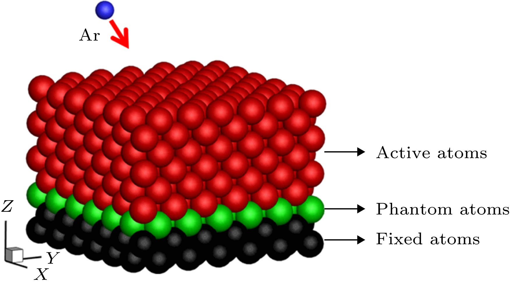
图 1 气体分子在固体表面散射的物理模型
Figure 1. Physical model for scattering gas molecules on solid surfaces.
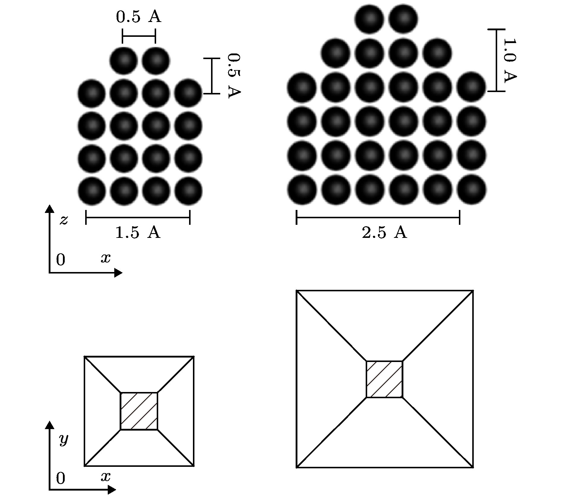
图 2 表面粗糙度的纳米构型
Figure 2. Schematic diagram of the roughness geometry.
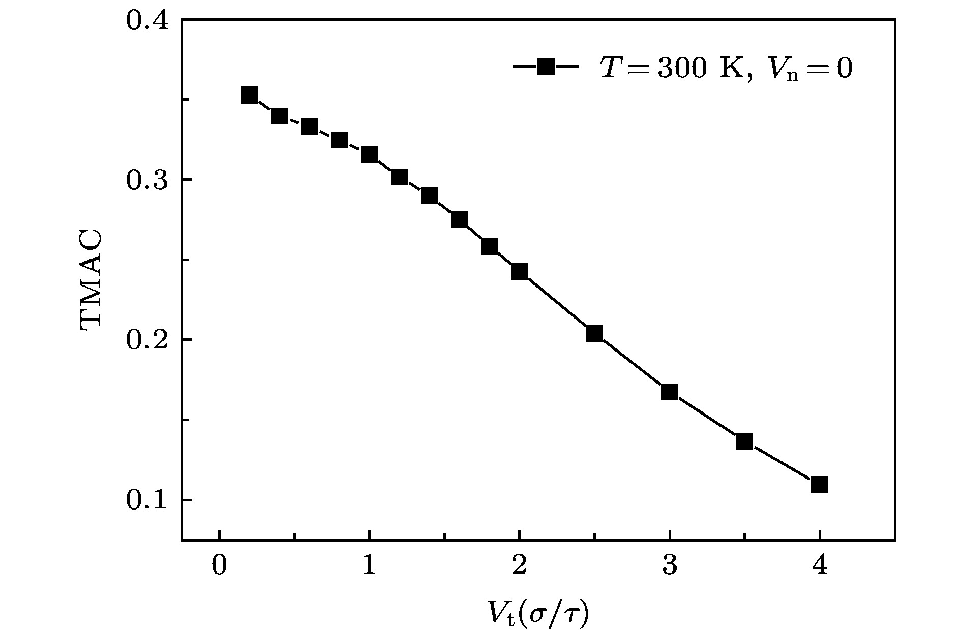
图 3 不同宏观切向速度下的切向动量适应系数
Figure 3. TMAC values of gas molecular under different macroscopic tangential velocities.
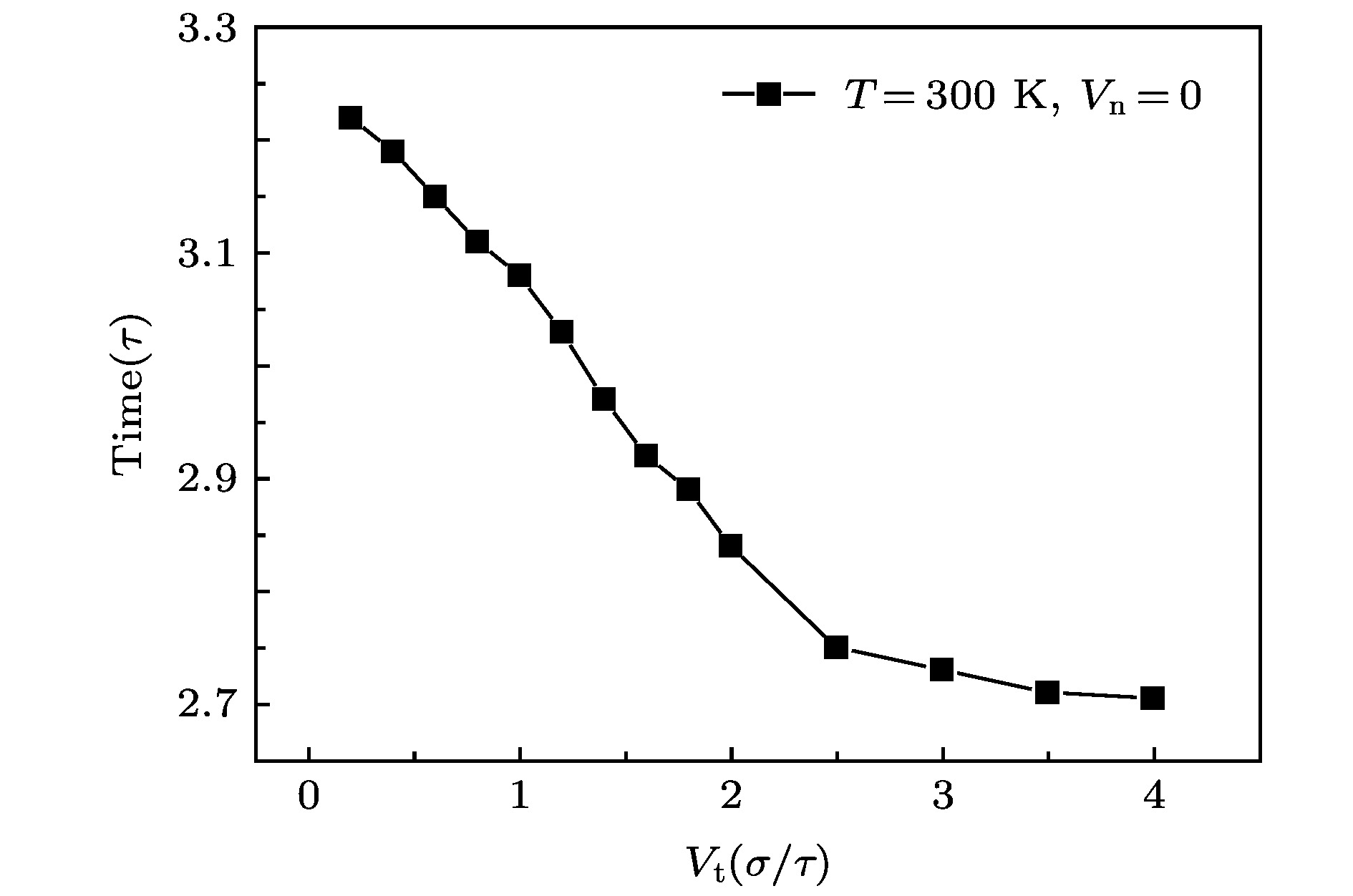
图 4 不同宏观切向速度下气体分子与表面作用时间
Figure 4. Time of gas-solid interaction under different macroscopic tangential velocities.
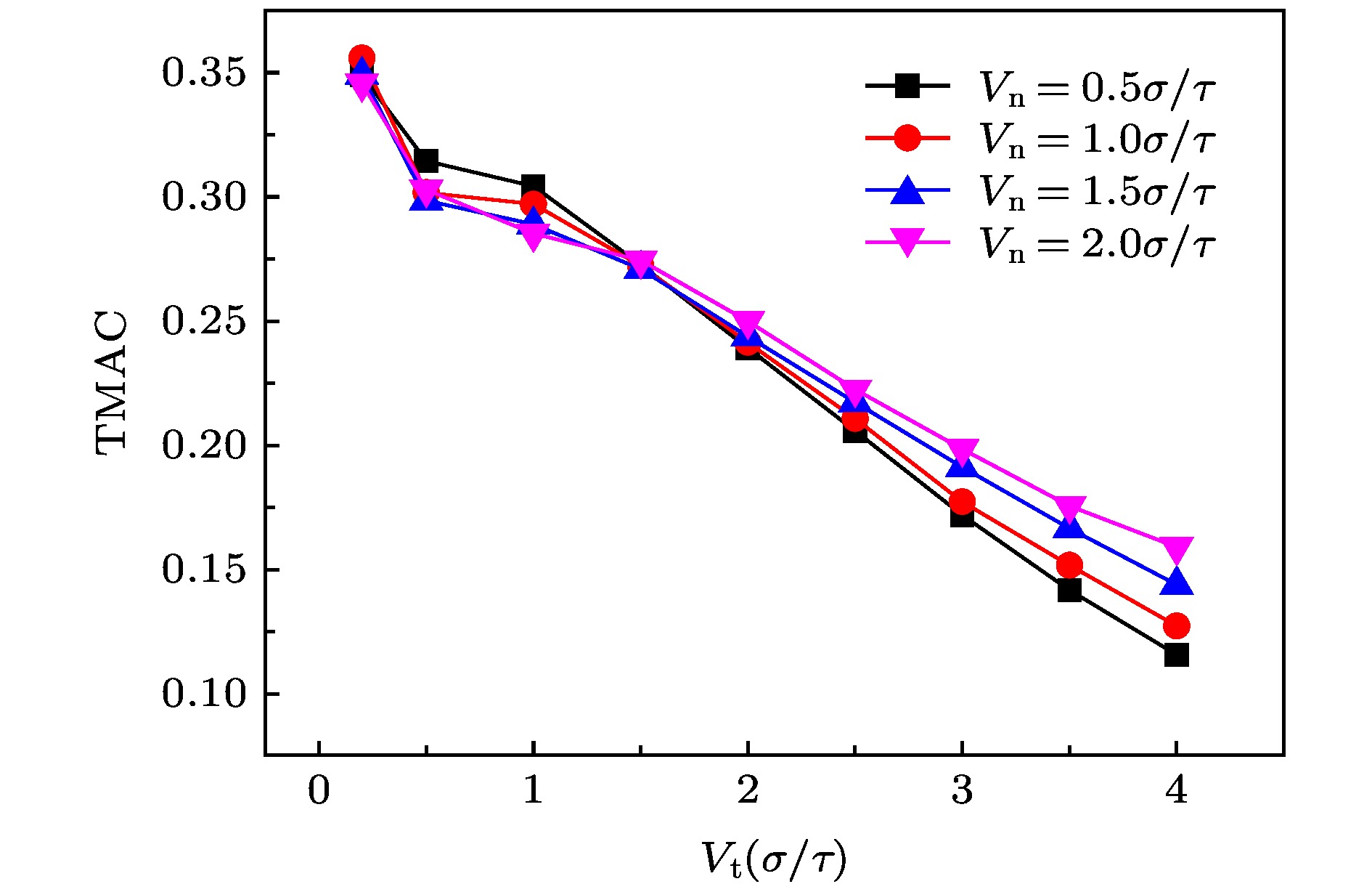
图 5 不同宏观切向速度及法向速度下的切向动量适应系数
Figure 5. TMAC values of gas molecular under different macroscopic tangential and normal velocities.
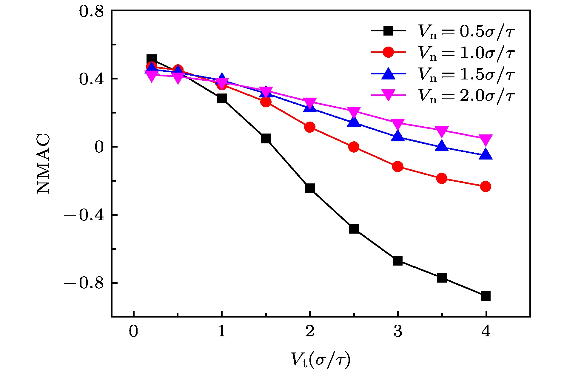
图 6 不同宏观切向速度及法向速度下的法向动量适应系数
Figure 6. NMAC values of gas molecular under different macroscopic tangential and normal velocities.
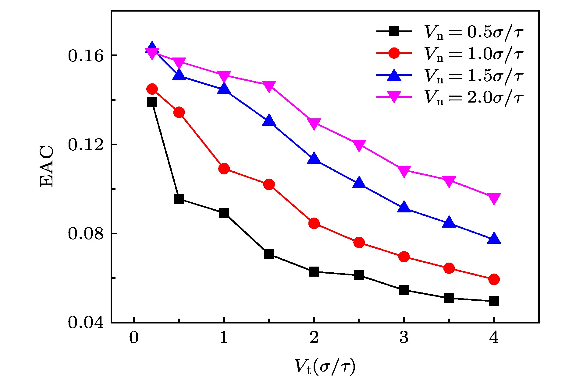
图 7 不同宏观切向及法向速度下的法向能量适应系数
Figure 7. EAC values of gas molecular under different macroscopic tangential and normal velocities.
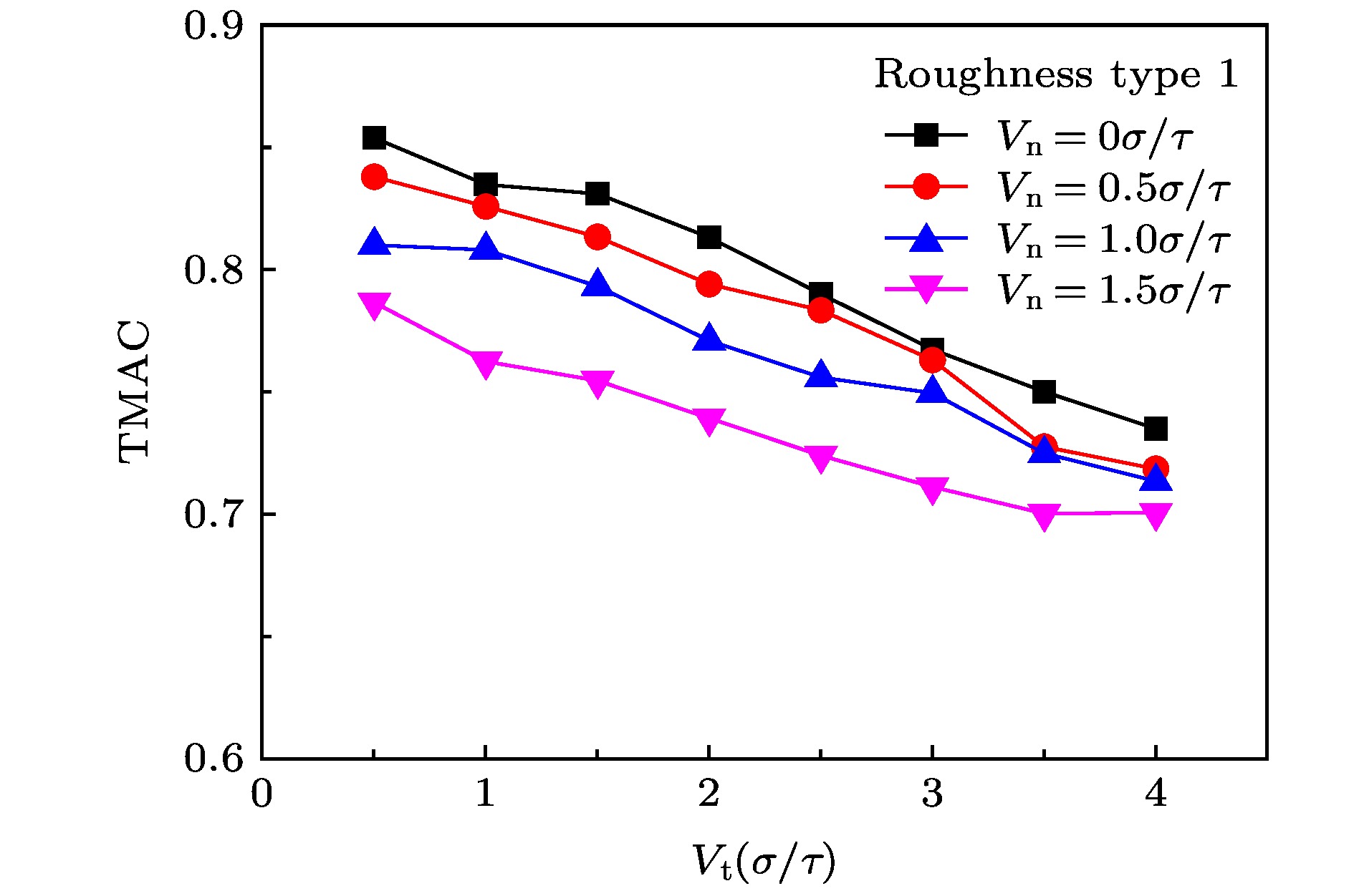
图 8 粗糙度为0.5 A的粗糙表面下, 不同宏观切向速度及法向速度下的切向动量适应系数
Figure 8. TMAC values of gas molecular on rough surfaces of 0.5 A under different macroscopic tangential and normal velocities
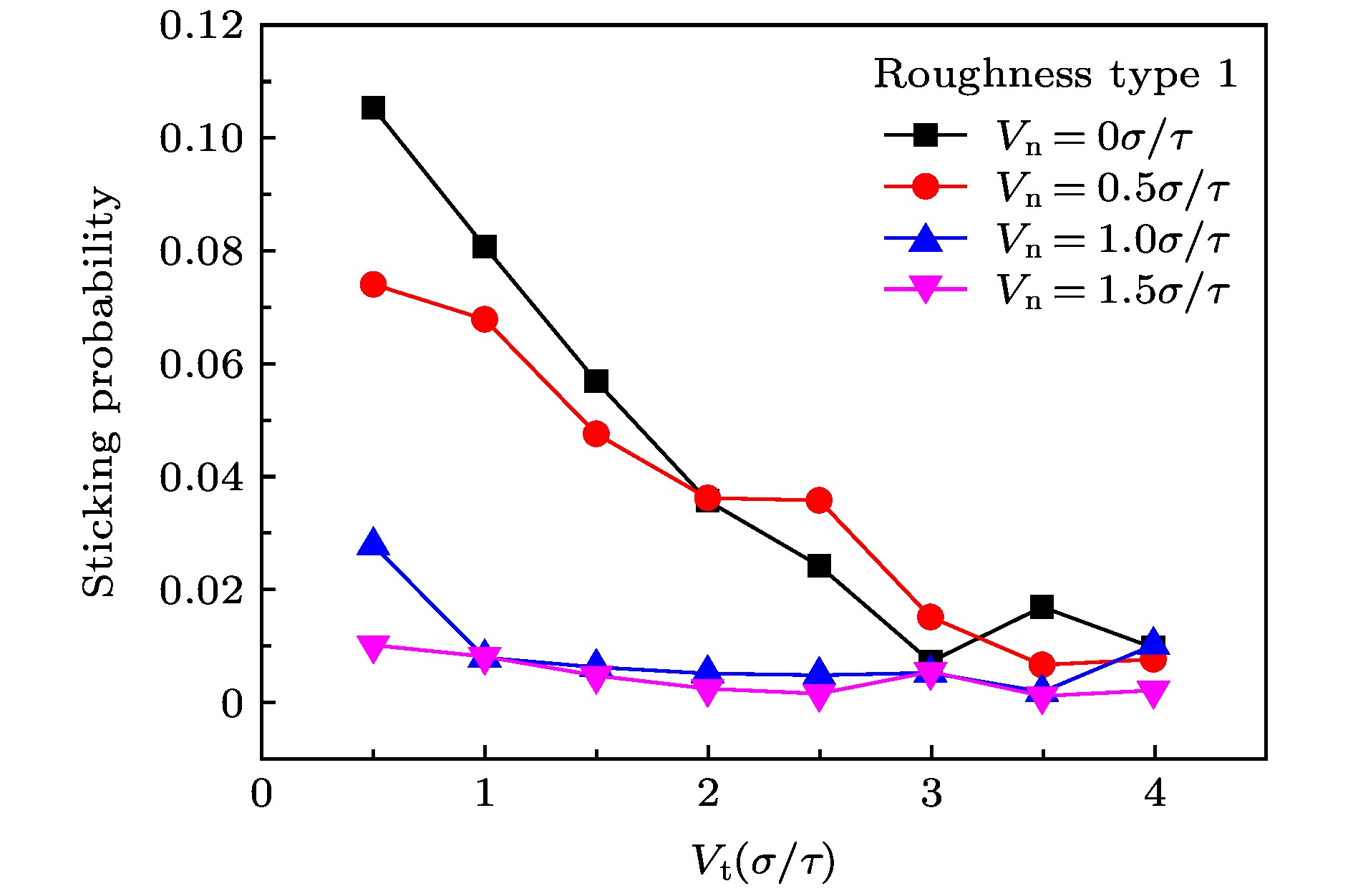
图 9 粗糙度为0.5 A的粗糙表面下, 不同宏观切向速度及法向速度下的气体分子吸附概率
Figure 9. Sticking probability of gas molecular on rough surfaces of 0.5 A under different macroscopic tangential and normal velocities.
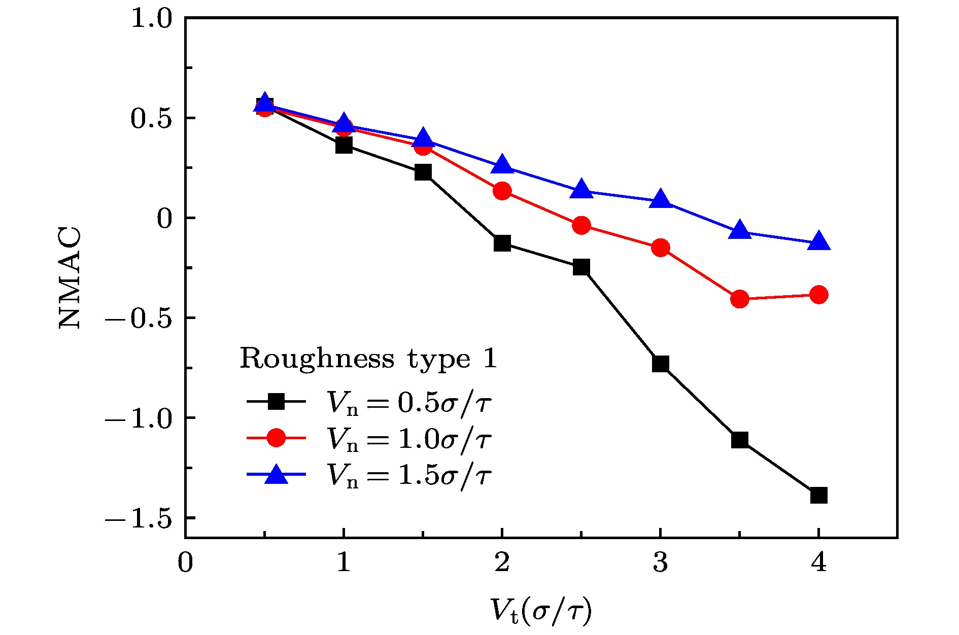
图 10 粗糙度为0.5 A的粗糙表面下, 不同宏观切向速度及法向速度下的法向动量适应系数
Figure 10. NMAC values of gas molecular on rough surfaces of 0.5 A under different macroscopic tangential and normal velocities.
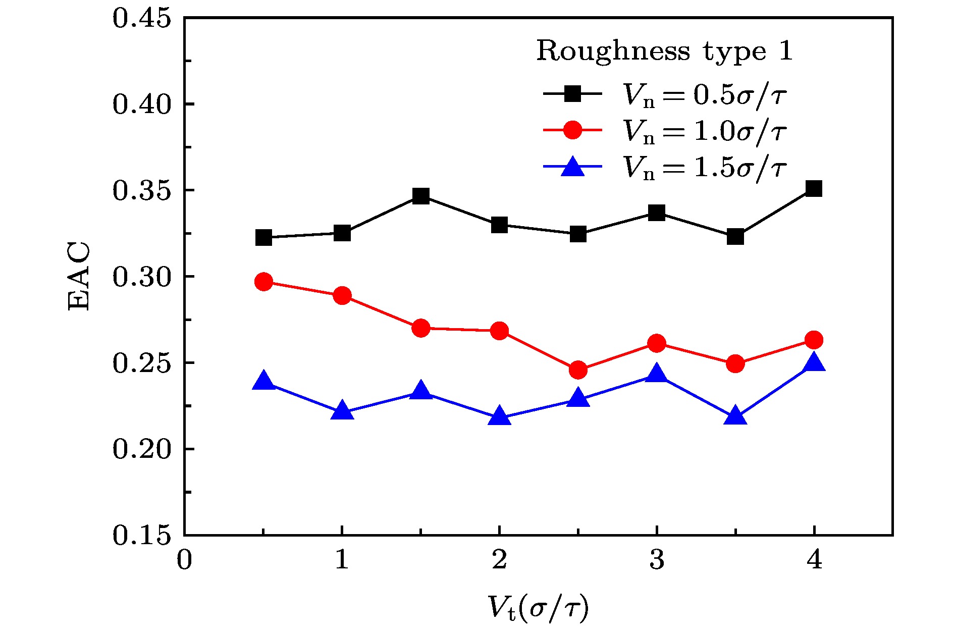
图 11 粗糙度为0.5 A的粗糙表面下, 不同宏观切向速度及法向速度下的能量适应系数
Figure 11. EAC values of gas molecular on rough surfaces of 0.5 A under different macroscopic tangential and normal velocities.
图 12 粗糙度为1.0 A的粗糙表面下, 不同宏观切向速度及法向速度下的切向动量适应系数
Figure 12. TMAC values of gas molecular on rough surfaces of 1.0 A under different macroscopic tangential and normal velocities.
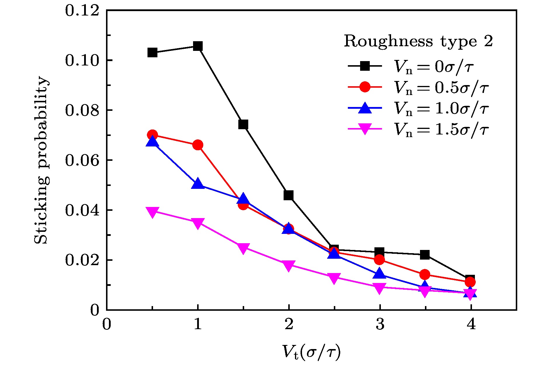
图 13 粗糙度为1.0 A的粗糙表面下, 不同宏观切向速度及法向速度下的气体分子吸附概率
Figure 13. Sticking probability of gas molecular on rough surfaces of 1.0 A under different macroscopic tangential and normal velocities.
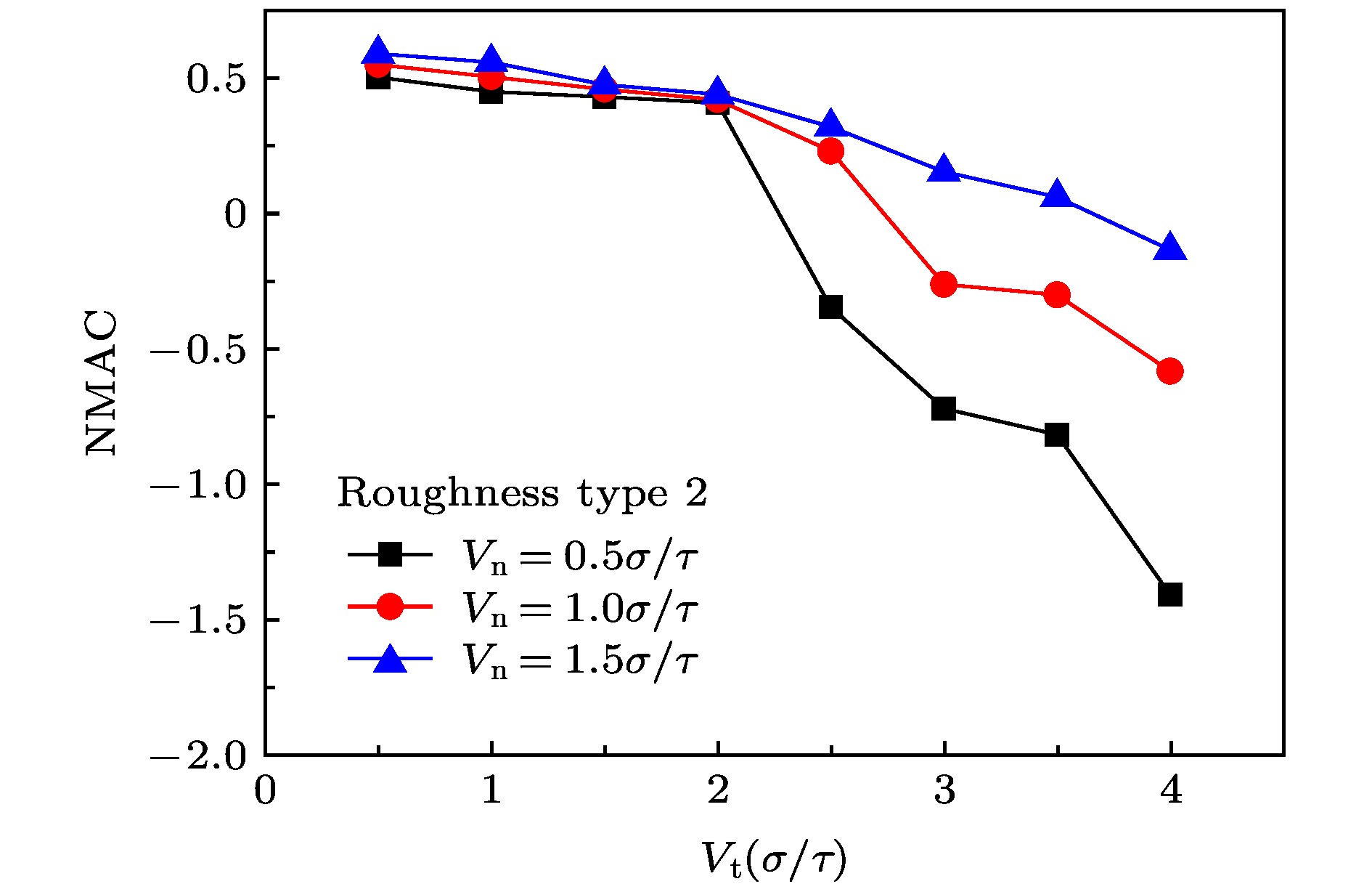
图 14 粗糙度为1.0 A的粗糙表面下, 不同宏观切向速度及法向速度下的法向动量适应系数
Figure 14. NMAC values of gas molecular on rough surfaces of 1.0 A under different macroscopic tangential and normal velocities.
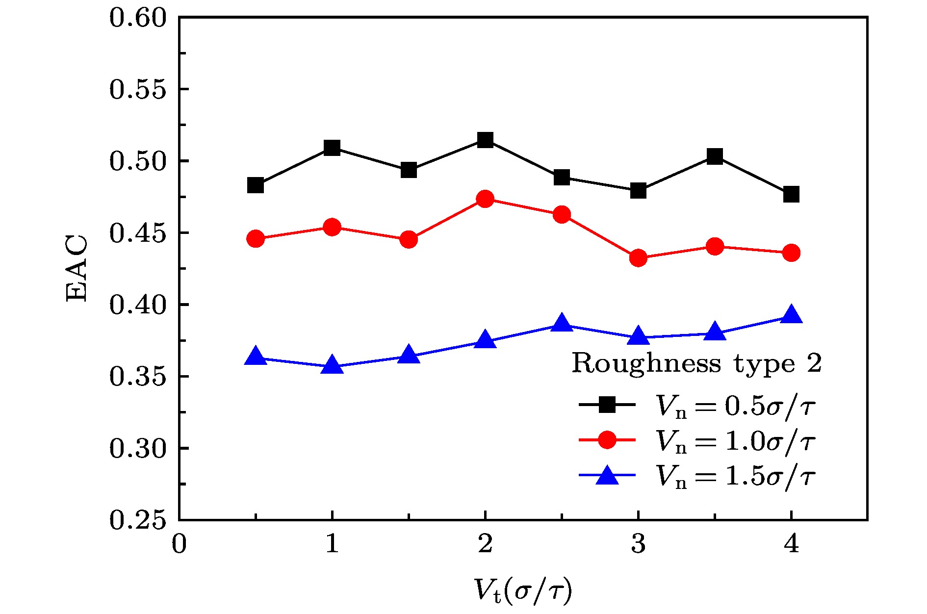
图 15 粗糙度为1.0 A的粗糙表面下, 不同宏观切向速度及法向速度下的能量适应系数
Figure 15. EAC values of gas molecular on rough surfaces of 1.0 A under different macroscopic tangential and normal velocities.
表 1 分子动力学模拟中的参数
Table 1. Parametersin the MD simulations.
相互作用 $\sigma {\rm{/nm}}$ $\varepsilon {\rm{/J}}$ mass/kg Ar-Ar 0.3405 $1.670 \times {10^{-{\rm{21}}}}$ $6.633 \times {10^{-{\rm{26}}}}$ Pt-Pt 0.2770 $52.07 \times {10^{ -{\rm{21}}}}$ $32.36 \times {10^{-{\rm{26}}}}$ Ar-Pt 0.3085 $0.894 \times {10^{ - {\rm{21}}}}$ —  DownLoad: CSV
-
[1] Verbridge S S, Craighead H G, Parpia J M 2008 Appl. Phys. Lett. 92 013112
Google Scholar
[2] Zhang Z Q, Zhang H W, Ye H F 2009 Appl. Phys. Lett. 95 154101
Google Scholar
[3] Song H Q, Yu M X, Zhu W Y, Zhang Y, Jiang S X 2013 Chin. Phys. Lett. 30 014701
Google Scholar
[4] Rovenskaya O I 2015 Int. J. Heat Mass Tran. 89 1024
Google Scholar
[5] Bao F B, Huang Y L, Zhang Y H, Lin J Z 2015 Microfluid Nanofluid 18 1075
Google Scholar
[6] Cao B Y, Sun J, Chen M, Guo Z Y 2009 Int. J. Mol. Sci. 10 4638
Google Scholar
[7] Bird G A 1994 Molecular Gas Dynamics and the Direct Simulation of Gas Flows (Oxford: Oxford University Press) pp199−206
[8] Fan J, Shen C 2001 J. Comput. Phys. 167 393
[9] Yuan Y D, Rahman S 2016 Physica A 463 25
Google Scholar
[10] Verbeek M G 2018 Microfluid. Nanofluid. 22 34
Google Scholar
[11] Maxwell J C 1879 Phil. Trans. R. Soc. Lond. 170 231
Google Scholar
[12] Cercignani C, Lampis M 1971 Transp. Theory Stat. Phys. 1 101
Google Scholar
[13] Lord R G 1991 Phys. Fluids 3 706
Google Scholar
[14] Agrawal A, Prabhu S V 2008 J. Vac. Sci. Technol. A 26 634
[15] Yakunchikov A N, Kovalev V L, Utyuzhnikov S V 2012 Chem. Phys. Lett. 554 225
Google Scholar
[16] Zhang W, Meng G, Wei X 2012 Microfluid. Nanofluid. 13 845
Google Scholar
[17] Zhang H W, Zhang Z Q, Zheng Y G, Ye H F 2010 Phys. Rev. E 81 066303
Google Scholar
[18] Rapaport D C 2004 The Art of Molecular Dynamics Simulation (New York: Cambridge University Press) pp4−5
[19] Bao F B, Huang Y L, Qiu L M, Lin J Z 2015 Mol. Phys. 113 561
Google Scholar
[20] Spijker P, Markvoort A J, Nedea S V, Hilbers P A 2010 Phys. Rev. E 81 011203
Google Scholar
[21] Bruno D, Cacciatore M, Longo S, Rutigliano M 2000 Chem. Phys. Lett. 320 245
Google Scholar
[22] Kovalev V, Yakunchikov A, Li F 2011 Acta Astronaut. 69 744
Google Scholar
[23] Dongari N, Zhang Y H, Reese J M 2012 AIP Conf. Proc. 1501 895
[24] Cao B Y, Chen M, Guo Z Y 2005 Appl. Phys. Lett. 86 091905
Google Scholar
[25] Finger G W, Kapat J S, Bhattacharya A 2007 J. Fluids Eng. 129 31
[26] Sun J, Li Z X 2008 Mol. Phys. 106 2325
Google Scholar
[27] Sun J, Li Z X 2009 Mol. Simul. 35 228
Google Scholar
[28] Sun J, Li Z X 2010 Comput. Fluids 39 1345
Google Scholar
[29] Prabha S K, Sathian S P 2012 Comput. Fluids 68 47
[30] Pham T T, To Q D, Lauriat G, Leonard C 2012 Phys. Rev. E 86 051201
Google Scholar
[31] Liang Z, Keblinski P 2014 Int. J. Heat Mass Tran. 78 161
Google Scholar
[32] Reinhold J, Veltzke T, Wells B, Schneider J, Meierhofer F, Colombi Ciacchi L, Chaffee A 2014 Comput. Fluids 97 31
Google Scholar
[33] Lim W W, Suaning G J, McKenzie D R 2016 Phys. Fluids 28 097101
Google Scholar
[34] Yamaguchi H, Matsuda Y, Niimi T 2017 Phys. Rev. E 96 013116
Google Scholar
[35] 张冉, 谢文佳, 常青, 李桦 2018 物理学报 67 084701
Google Scholar
Zhang R, Xie W J, Chang Q, Li H 2018 Acta Phys. Sin. 67 084701
Google Scholar
[36] Cao B Y, Chen M, Guo Z Y 2006 Int. J. Eng. Sci. 44 927
Google Scholar
[37] Xie J F, Cao B Y 2016 Mol. Simul. 43 65
[38] 张冉, 常青, 李桦 2018 物理学报 67 223401
Google Scholar
Zhang R, Chang Q, Li H 2018 Acta Phys. Sin. 67 223401
Google Scholar
[39] Maruyama S 2000 Advances in Numerical Heat Transfer (Vol.2) (Boca Raton : CRC Press) pp189
[40] 张烨, 张冉, 常青, 李桦 2019 物理学报 68 124702
Google Scholar
Zhang Y, Zhang R, Chang Q, Li H 2019 Acta Phys. Sin. 68 124702
Google Scholar
[41] Wu L, Bogy D B 2002 J. Tribol.-T. ASME 124 562
Google Scholar

 DownLoad:
Catalog
Metrics
- Abstract views: 13037
- PDF Downloads: 128
- Cited By: 0
