Search

Article

x

留言板

尊敬的读者、作者、审稿人, 关于本刊的投稿、审稿、编辑和出版的任何问题, 您可以本页添加留言。我们将尽快给您答复。谢谢您的支持!

姓名
邮箱
手机号码
标题
留言内容
验证码

The physics-based model of AlGaN/GaN high electron mobility transistor outer fringing capacitances

Liu Nai-Zhang Zhang Xue-Bing Yao Ruo-He

KE TING-SUI, CHOW PEN-LIEN. A STUDY ON THE ACOUSTIC INTERNAL FRICTION OF IRON VIBRATING TRANSVERSELY IN A STEADY MAGNETIC FIELD BY PIEZO-ELECTRIC CRYSTAL PLATES. Acta Phys. Sin., 1957, 13(2): 142-149. doi: 10.7498/aps.13.142
Citation: KE TING-SUI, CHOW PEN-LIEN. A STUDY ON THE ACOUSTIC INTERNAL FRICTION OF IRON VIBRATING TRANSVERSELY IN A STEADY MAGNETIC FIELD BY PIEZO-ELECTRIC CRYSTAL PLATES. Acta Phys. Sin., 1957, 13(2): 142-149. doi: 10.7498/aps.13.142

The physics-based model of AlGaN/GaN high electron mobility transistor outer fringing capacitances

Liu Nai-Zhang, Zhang Xue-Bing, Yao Ruo-He
Article Text (iFLYTEK Translation)
PDF
HTML
Get Citation
  • With the development of the application of AlGaN/GaN high electron mobility transistors in the radio frequency field, a capacitance model that can accurately describe the C-V characteristics of the device has become an important research topic. The gate capacitance of GaN HEMT can be divided into two parts: intrinsic capacitance and fringing capacitance related to two-dimensional electronic gas (2DEG) electrode. The fringing capacitance plays an important part in the switching device. The outer fringing capacitance Cofs/d dominates the fringing capacitance and is affected by the bias applied, especially the drain outer fringing capacitance Cofd. In order to establish the Cofd model which is related to the bias condition, the physics-based model of Cofd is established based on the conformal mapping, including the drain channel length variable. Since the drain channel length is related to the bias applied, the channel length modulation effect can be used to study how bias apllied effect the channel, and the relationship between Cofd and the bias condition is obtained. In addition, the threshold voltage variable is introduced when the channel length modulation effect is considered, and the threshold voltage drift caused by changes in the internal parameters and temperature of the device is studied using the threshold voltage variable in the model, and the relationship between Cofd and threshold voltage and temperature under different bias was obtained. It is found from the results of the study that as drain bias increases from zero, the channel length modulation effect keeps Cofd unchanged at lower drain bias. When the drain bias continues to increase, Cofd begins to decay again, and its decay rate slows down with the increase of gate bias. The decrease of donor impurity concentration and Al component in AlGaN barrier layer may increase the threshold voltage, which will strengthen the channel length modulation effect on Cofd, resulting in linear attenuation of Cofd. With the increasing of drain bias, the influence of threshold voltage shift on Cofd is enhanced, and the change of device operating temperature will enhance the threshold voltage shift and cause the deviation of Cofd. Moreover, with the continuous increase of drain bias, Cofd becomes more sensitive to the temperature variation.
      Corresponding author: Yao Ruo-He, phrhyao@scut.edu.cn

    半导体纳米晶体, 特别是ZnS/CdS核/壳纳米晶, 已广泛应用于照明和显示领域、激光、太阳能浓度、光催化、光电探测器、光学信息存储和生物成像[1-3]. 对ZnS/CdS纳米异质结构和电子性质进行研究, 可用于控制光的偏振, 热稳定性, 光催化活性[4]. 由于ZnS和CdS半导体的量子效应, 导致其具有新颖的光学和电子特性, 从而受到广泛的关注[5]. 这些半导体在发光二极管、光电器件、光催化、太阳能电池、电荷存储器、激光器、发光纳米复合材料和医疗诊断试剂等领域具有潜在的应用价值[6], 人们采用反胶束体系合成不同的纳米结构[7]. 然而, 硫醇结合可以钝化硫化物颗粒表面上的硫空位, 并改变它们的表面性质. 此外, 科研工作者采用不同的方法合成ZnS和CdS纳米结构, 例如在聚合物中嵌入分子筛并防止有机位点沉淀[8]. Purusothaman等[9]用密度泛函理论(DFT)计算能带CdS和ZnS, 此外, 他们还研究了温度对沉积在玻璃基板上的CdS纳米结构和光学性质的影响. 近年来, 科研工作者已经合成和表征各种半导体核-壳纳米结构, 例如CdSe/ZnS, CdSe/CdS, CdS/ZnS, CdS/ZnS/SiO2[10], 制备这些核/壳纳米晶、纳米异质结是为了能产生新颖的光电性能, 但是, 这些纳米材料没有铁磁性, 有些掺杂的纳米材料能产生铁磁性, 主要集中在Fe, Co, Ni这些元素上[11,12], Fe, Co, Ni本身是磁性元素, 即使能使纳米材料产生铁磁性, 也不足为奇, 并且方法一般较复杂. 然而, 用溶剂热法制备纳米材料, 方法简单, 成本低下, 有关溶剂热法合成Cr掺杂ZnS和CdS纳米结构的报道却很少. 有关Cr掺杂的ZnS和CdS纳米结构能在室温下产生铁磁性的报道少之又少, 并且Cr是非磁性元素, Cr掺杂ZnS和CdS纳米结构能在室温下产生铁磁性, 有重要的应用价值, 对铁磁性产生的来源, 目前还在研究中.

    本文用溶剂热法制备出Cr掺杂ZnS和CdS纳米结构, 研究了结构、形貌、化学成分以及室温铁磁性. 当Cr的含量达到原子百分比为7.25%或4.31%时, Cr掺杂花状ZnS垂直堆叠, 厚度为220—290 nm. 不同Cr掺杂ZnS和CdS纳米结构表现出室温铁磁性, 而纯ZnS纳米结构表现出明显的抗磁性. Cr掺杂ZnS(Cr原子百分比为4.31%, 7.25%)和CdS(Cr原子百分比为1.84%, 2.12%)的饱和磁化强度Ms分别为2.314 × 10⁻³, 5.683 × 10⁻³, 2.351 × 10⁻³和7.525 × 10⁻³ emu/g (1 emu/g = 10–3A·m2/g). Cr掺杂的ZnS和CdS纳米结构的铁磁性起源与掺杂产生的结构缺陷有关.

    实验中使用的化学试剂是分析纯试剂, 无需进一步提纯即可使用, 使用的有机溶液为乙醇胺(EA)和乙二胺(EN). 本实验在前期实验基础上, 不断优化实验参数. 典型的实验步骤如下: 为了合成不同Cr掺杂量的纤锌矿ZnS纳米片, 将1 mmol氧化锌(ZnO)和1 mmol硫粉(S)溶解在10 mL乙二胺和20 mL乙醇胺的混合溶剂中, 向混合溶剂内加入0.025 mmol草酸, 将混合物磁力搅拌10 min后, 再向混合物中加入0.250 mmol六水氯化合物(CrCl3·6H2O). 将混合物搅拌15 min, 然后转移到40 mL聚四氟乙烯内衬的不锈钢反应釜中, 继续搅拌15 min. 密封后, 在30 min内, 将高压釜加热到200 ℃并在该温度下保持24 h, 最后自然冷却至室温. 收集沉淀物, 用无水乙醇和去离子水洗涤数次, 在60 ℃下, 真空箱中干燥6 h. 用类似的合成方法制备其他样品, 将制备的样品分别记录为样品A—样品F, 如表1所列.

    表 1  制备样品(A—F)的反应条件(所有实验在200 ℃下反应24 h)
    Table 1.  Reaction conditions of the prepared products (All experments are carried out 200 ℃ for 24 h).
    SampleCompsition of solvent/mLSulfur, zinc and cadium source/mmolChromic chloride hexahydrate/mmolConcentration of oxalic acid/mmol
    A10 EN + 20 EA1 S + 1 ZnO0.2500.025
    B20 EN + 10 EA1 S + 1 ZnO0.5000.025
    E15 EN + 15 EA1 S + 1 ZnO00.025
    C10 EN + 20 EA1 S + 1 CdO0.2500.025
    D20 EN + 10 EA1 S + 1 CdO0.5000.025
    F15 EN + 15 EA1 S + 1 CdO00.025
    下载: 导出CSV 
    | 显示表格

    样品的晶体结构和化学成分用X-射线衍射(XRD)(Mac Science M18XHF22-SRA, Cu Kα靶, λ = 0.154 nm)表征; 样品的形貌由扫描电子显微镜(SEM)(Philips XL-30)表征; 通过电子能量散射谱(EDS)测量样品的化学组成, 通过振动样品磁强计(VSM, Lake 7400)表征样品的磁性能.

    通过XRD方法分析晶体结构和化学组成, 图1是Cr掺杂ZnS纳米片的XRD图谱, 三条曲线分别对应样本A (Cr原子百分比为4.31%, a); 样本B (Cr原子百分比为7.25%, b); 样本E (Cr原子百分比为0.00%, e). 图2是Cr掺杂CdS纳米片的XRD图谱, 三条曲线分别对应样本C (Cr原子百分比为1.84%, c); 样本D (Cr原子百分比为2.12%, d); 样本F (Cr原子百分比为0.00%, f). Cr掺杂ZnS的衍射峰位2θ是27.91°, 32.72°, 47.43°, 56.98°, 58.76°, 68.87°和76.90°, 与 (111), (200), (220), (311), (222), (400) 和(331) 六方纤锌矿ZnS晶面相对应, 这与[PDF 65-16917(ICCD, 2002), a = 0.3820 nm, c = 0.6257 nm]相一致. Cr掺杂CdS的衍射峰位2θ是24.70°, 26.32°, 28.55°, 37.14°, 43.66°, 48.28°, 52.23°和54.60°, 与(100), (002), (101), (102), (110), (103), (112) 和(201) 六方纤锌矿CdS的晶面相对应, 这与[PDF 41-1049 (ICCD, 2002), a = 0.4150 nm, c = 0.6750 nm]相一致. 图1图2中未发现Cr2S3或任何其他第二相, 这表明Cr3+在一定程度上掺入到ZnS和CdS晶格中. 如图1所示, 在仪器分辨范围内, Cr掺杂ZnS的(111)峰位置相对于纯ZnS的(111)峰位置稍微向低角度移动了0.2°, 这证实了Cr3+掺入ZnS晶格中, 而Cr掺杂CdS的(100)峰值位置相对于未掺杂的CdS的(100)稍微向高角度移0.3°, 如图2所示. Cr掺杂ZnS的(111)特征峰峰强度和峰宽均增大, 表明纳米结构在生长. 众所周知, 晶格发生变化, 是由于半径为Cr3+ (RCr = 0.0890 nm)的离子, 有效取代半径为Zn2+或Cd2+(RZn = 0.0740 nm, RCd = 0.0970 nm)的离子效应产生的. 根据布拉格衍射公式(2dsinθ=kλ)可以证实有少量Cr掺入ZnS和CdS晶格中.

    图 1 Cr掺杂ZnS纳米片的XRD图谱, 三条曲线分别对应样本A (Cr原子百分比为4.31%, a), 样本B (Cr原子百分比为7.25%, b)和样本E (Cr原子百分比为0.00%, e)\r\nFig. 1. Some of the powder XRD patterns of Cr-doped ZnS nanosheets. Three curves correspond to sample A (atomic percentages of Cr is4.31%, a), sample B (atomic percentages of Cr is 7.25%, b), sample E (atomic percentages of Cr is 0%, e), respectively.
    图 1  Cr掺杂ZnS纳米片的XRD图谱, 三条曲线分别对应样本A (Cr原子百分比为4.31%, a), 样本B (Cr原子百分比为7.25%, b)和样本E (Cr原子百分比为0.00%, e)
    Fig. 1.  Some of the powder XRD patterns of Cr-doped ZnS nanosheets. Three curves correspond to sample A (atomic percentages of Cr is4.31%, a), sample B (atomic percentages of Cr is 7.25%, b), sample E (atomic percentages of Cr is 0%, e), respectively.
    图 2 Cr掺杂CdS纳米片的XRD图谱, 三条曲线分别对应样本C (Cr原子百分比为1.84%, c), 样本D (Cr原子百分比为2.12%, d)和样本F (Cr原子百分比为0.00%, f)\r\nFig. 2. Some of the powder XRD patterns of the Cr-doped CdS nanosheets. Three curves correspond to sample C (atomic percentages of Cr is 1.84%, c), sample D (atomic percentages of Cr is 2.12%, d) and sample F (atomic percentages of Cr is 0.00%, f), respectively.
    图 2  Cr掺杂CdS纳米片的XRD图谱, 三条曲线分别对应样本C (Cr原子百分比为1.84%, c), 样本D (Cr原子百分比为2.12%, d)和样本F (Cr原子百分比为0.00%, f)
    Fig. 2.  Some of the powder XRD patterns of the Cr-doped CdS nanosheets. Three curves correspond to sample C (atomic percentages of Cr is 1.84%, c), sample D (atomic percentages of Cr is 2.12%, d) and sample F (atomic percentages of Cr is 0.00%, f), respectively.

    图3(a), 图3(b)图3(e) 给出了Cr掺杂ZnS的SEM图案, 掺杂Cr的原子百分比分别为4.31%, 7.25%, 0. 图3(c), 图3(d)图3(f)给出了Cr掺杂CdS的SEM图案, 掺杂Cr的原子百分比分别为1.84%, 2.12%, 0. Cr掺杂ZnS的形貌主要由高产量的纳米片组成, 通过对比Cr掺杂ZnS纳米片(图3(a), 图3(b)图3(e))的样品, 可以看出纳米片的形貌取决于Cr掺杂量的多少. 当Cr含量的原子百分比为4.31%或7.25%时, Cr掺杂ZnS纳米片像花状一样, 垂直堆叠, 厚度约为210—290 nm, 未掺杂ZnS的形貌由相对较厚的纳米片组成. Cr掺杂CdS的形貌主要是纳米片, 通过比较Cr掺杂CdS纳米片(图3(c), 图3(d)图3(f)) 的样品, 可以看出纳米片的形貌与Cr掺杂量多少无关, 不同Cr掺杂CdS的形貌由厚度约为120—190 nm的雪花状纳米片组成. ZnS具有与ZnO相同的六方纤锌矿晶体结构. Kumar等[13]和Cheng等[14]报道, 用Cr掺杂ZnO纳米晶体时, 使得形态从一维(1D)NPC向二维(2D)NS急剧演变, 值得注意的是, 在未掺杂和Cr掺杂ZnO纳米晶体生长期间, 所有成核和沉淀条件是相同的. 因此, 1D到2D纳米晶体的形貌转变不是沉淀和成核条件的结果, 而是掺杂剂Cr3+阳离子作用的结果. 掺杂Y3+离子导致ZnO从1D ZnO纳米棒到2D ZnO纳米片的类似形态演变[15]. 将Cr3+离子(源于CrCl3·6H2O)引入溶液中, 形成CrO2阴离子单元掺杂剂. 可能的形成路线可表示为: Cr3+ + OH → Cr(OH)3 + OHCrO2. 在[001]面上, CrO2的阴离子单元掺杂剂与正电Zn2+金属离子中和, 从而抑制[001]方向生长. 在上述分析的基础上, 提出了混合溶剂中Cr掺杂ZnS生长过程可能形成机理如下:

    图 3 (a), (b), (e) Cr掺杂ZnS纳米片的SEM图案; (c), (d), (f) Cr掺杂CdS纳米片的SEM图案, 掺杂Cr的原子百分比分别为(a) 4.31%, (b) 7.25%, (e) 0, (c) 1.84%, (d) 2.12%, (f) = 0\r\nFig. 3. (a), (b), (e) The SEM patterns of the Cr-doped ZnS nanosheets; (c), (d), (f) the SEM patterns of the Cr-doped CdS nanosheets. The atomic percentages of Cr doping are (a) 4.31%, (b) 7.25%, (e) 0, (c) 1.84%, (d) 2.12%, (f) 0, respectively.
    图 3  (a), (b), (e) Cr掺杂ZnS纳米片的SEM图案; (c), (d), (f) Cr掺杂CdS纳米片的SEM图案, 掺杂Cr的原子百分比分别为(a) 4.31%, (b) 7.25%, (e) 0, (c) 1.84%, (d) 2.12%, (f) = 0
    Fig. 3.  (a), (b), (e) The SEM patterns of the Cr-doped ZnS nanosheets; (c), (d), (f) the SEM patterns of the Cr-doped CdS nanosheets. The atomic percentages of Cr doping are (a) 4.31%, (b) 7.25%, (e) 0, (c) 1.84%, (d) 2.12%, (f) 0, respectively.
    Zn2++xEN[Zn(EN)x]2+,
    (1)
    Zn2++yEA[Zn(EA)y]2+,
    (2)
    Zn2++S2ZnS,
    (3)
    (1x)Zn2++S2+xCr2+Zn1xCrxS.
    (4)

    在溶剂热过程之前, 混合溶液作用下的Zn源主要以[Zn(EN)x]2+和[Zn(EA)y]2+离子形式存在, 其余Zn源以Zn2+离子形式存在(反应(1)和(2)), 这有助于控制反应混合物中Zn2+的浓度. 当混合溶液被加热时, S缓慢而均匀地分解形成S2–离子(反应(3)). 在下一步中, S2–离子将与Zn2离子和Cr3+离子反应形成Zn1–xCrxS, 如反应(4)中所示. 当Zn1–xCrxS浓度达到过饱和时, Zn1–xCrxS晶核按照Zn1–xCrxS晶体的生长习性形成和生长. 同样, Cr掺杂CdS具有相似的过程. 晶核沿[001]方向的生长受到限制, 导致有效的横向生长, 这导致形成2D Cr掺杂的ZnS-NS. 用纳米片组装的三维(3D)分层花状Cr-ZnS产品与未掺杂ZnS纳米棒的形貌完全不同, 并且这种变化可能导致2D NS与1D NPC相比, 产生许多新特征和新性能.

    图4(a)图4(b)给出了Cr掺杂ZnS的EDS图, 表明合成的产物由Cr, Zn和S组成. 图4(c)图4(d)给出了Cr掺杂CdS的EDS图, 结果表明, 合成产物由Cr, Cd和S组成. 在系统中, 采集的谱是点分析, 探测到Cr的存在, 这证明Cr3+离子掺入ZnS和CdS晶格中. 基于EDS的测量和计算, Cr掺杂ZnS纳米片中Cr含量的原子百分比分别为4.31%和7.25%, 计算Cr掺杂CdS纳米片中Cr的含量, 原子百分比分别为1.84%和2.12%. 准确可靠地测定Cr掺杂ZnS和CdS的电学性能和表面应变, 对于预测其在纳米电子和光学器件中的潜在应用具有重要意义. 同时, 纳米晶体的体积变化是由应变张量的分量引起的. 考虑到Cr掺杂ZnS和CdS的纳米结构, 连续弹性理论(CET)允许半导体的界面应变如下[16]:

    图 4 (a), (b) Cr掺杂ZnS纳米片的EDS图; (c), (d) Cr掺杂CdS纳米片的EDS图. 掺杂Cr的原子百分比分别为(a) 4.31%, (b) 7.25%, (c) 1.84%, (d) 2.12%\r\nFig. 4. (a), (b) The EDS patterns of the Cr-doped ZnS nanosheets; (c), (d) the EDS patterns of the Cr-doped CdS nanosheets. The atomic percentages of Cr doping are (a) 4.31%, (b) 7.25%, (c) 1.84%, (d) 2.12%, respectively.
    图 4  (a), (b) Cr掺杂ZnS纳米片的EDS图; (c), (d) Cr掺杂CdS纳米片的EDS图. 掺杂Cr的原子百分比分别为(a) 4.31%, (b) 7.25%, (c) 1.84%, (d) 2.12%
    Fig. 4.  (a), (b) The EDS patterns of the Cr-doped ZnS nanosheets; (c), (d) the EDS patterns of the Cr-doped CdS nanosheets. The atomic percentages of Cr doping are (a) 4.31%, (b) 7.25%, (c) 1.84%, (d) 2.12%, respectively.
    εrr=εθθ=εφφ=ε=3Bc0εm/(3Bc0+4μs),
    (5)

    其中εrr, εθθεφφ是纳米晶体坐标中的应变分量. εm定义为纳米晶界面处的平均晶格百分比差异[17],

    εm=2(asac)/(as+ac),
    (6)

    其中asac分别是晶体Cr掺杂ZnS和CdS半导体的晶格常数; Bco是Cr掺杂ZnS和CdS半导体的弹性模量; μs是Cr掺杂ZnS和CdS半导体的剪切模量.

    利用a(εm)=a0(1εm)计算受影响的应变物的晶格参数, 用(6)式计算核心区域中的应变. 采用VSM方法测定室温下不同Cr含量的ZnS和CdS纳米片的磁性能.

    未掺杂ZnS纳米片表现出抗磁性, 如图5所示. 未掺杂CdS纳米片在室温下表现出弱的铁磁性, 如图6所示.

    图 5 未掺杂ZnS纳米片在室温下的磁化强度和磁场强度(M-H)曲线\r\nFig. 5. M-H curves of undoped ZnS nanosheets at room temperature.
    图 5  未掺杂ZnS纳米片在室温下的磁化强度和磁场强度(M-H)曲线
    Fig. 5.  M-H curves of undoped ZnS nanosheets at room temperature.
    图 6 未掺杂CdS纳米片在室温下的磁化强度和磁场强度(M-H)曲线\r\nFig. 6. M-H curves of undoped CdS nanosheets at room temperature.
    图 6  未掺杂CdS纳米片在室温下的磁化强度和磁场强度(M-H)曲线
    Fig. 6.  M-H curves of undoped CdS nanosheets at room temperature.

    然而, Cr掺杂ZnS和CdS纳米片具有明显的磁滞回线, 这充分表明Cr掺杂ZnS和CdS纳米片在室温下具有铁磁性, 如图7所示. Cr掺杂ZnS (Cr原子百分比为4.31%和7.25%)纳米片的饱和磁化强度(Ms)分别为2.314 × 10⁻³和5.683 × 10⁻³ emu/g, 矫顽力(Hc) 分别为74.631, 114.372和64.349 Oe. Cr掺杂CdS (Cr原子百分比为0, 1.84%和2.12%) 纳米片的饱和磁化强度(Ms)分别为0.854 × 10⁻³, 2.351 × 10⁻³和7.525 × 10⁻³ emu/g, 矫顽力(Hc)分别为74.631, 114.372和64.349 Oe. 图8给出Cr掺杂ZnS和CdS纳米片的饱和磁化强度(Ms)和矫顽力(Hc)的直方图. 表2是SEM, EDS和VSM计算Cr掺杂ZnS和CdS纳米片的Cr含量、形貌、尺寸、磁性、矫顽力和饱和磁化强度.

    图 7 Cr掺杂ZnS和CdS纳米片在室温下磁化强度和磁场强度(M-H)曲线\r\nFig. 7. M-H curves of Cr-doped ZnS and CdS nanosheets at room temperature.
    图 7  Cr掺杂ZnS和CdS纳米片在室温下磁化强度和磁场强度(M-H)曲线
    Fig. 7.  M-H curves of Cr-doped ZnS and CdS nanosheets at room temperature.
    图 8 Cr掺杂ZnS和CdS的饱和磁化强度(Ms)和矫顽力(Hc)的直方图\r\nFig. 8. Histogram of saturation magnetization (Ms) and coercivity (Hc) of Cr-doped ZnS and CdS nanosheets.
    图 8  Cr掺杂ZnS和CdS的饱和磁化强度(Ms)和矫顽力(Hc)的直方图
    Fig. 8.  Histogram of saturation magnetization (Ms) and coercivity (Hc) of Cr-doped ZnS and CdS nanosheets.
    表 2  SEM, EDS和VSM计算Cr掺杂的ZnS和CdS纳米片的Cr含量、形貌、尺寸、磁性、矫顽力和饱和磁化强度图
    Table 2.  Measured chromium content, morphology, size, magnetic properties, coercivity and saturation magnetization of Cr doped ZnS and CdS nanosheets using SEM, EDS and VSM.
    Cr content/%MorphologiesSize/nmMagnetic propertiesCoercivity/OeSaturation magnetization/ (10–3 emu·g–1)
    ZnS0Hexagonal flake310—390Diamagnetism
    4.31flower-like sheet210—290Ferromagnetism54.7212.314
    7.25Flower-like sheet200—250Ferromagnetism88.4415.683
    CdS0Snowflake110—160Weak ferromagnetism74.6310.854
    1.84Snowflake100—170strong ferromagnetism114.3722.351
    2.12Snowflake100—200Strong ferromagnetism64.3497.525
    下载: 导出CSV 
    | 显示表格

    随着Cr浓度的增加, Cr掺杂ZnS和CdS纳米片的饱和磁化强度也有所增加. Niwayama等[18]验证了Cr掺杂ZnTe纳米粒子的晶格常数和饱和磁化率随Cr浓度的增加呈线性增加, Haazen等[19]和Park等[20]讨论了Cr掺杂Bi2Se3和GaN的铁磁性质的起源. Li等[21]通过第一性原理计算了未掺杂ZnS为带隙为3.150 eV的非磁性半导体, Cr掺杂ZnS具有室温铁磁性, 这与之后的实验结果完全一致, Cr掺杂将少量杂质态引入ZnS的晶格区域内, 这种杂质态主要由Cr 3d态和S 3p态组成, 这两种态之间可以产生强杂化. 杂化意味着两个Cr原子之间的磁耦合是通过S原子之间的中介连接耦合作用. 为了符合Hund'rule法则, S 3p的状态应该是反铁磁的, 并且与两个相邻Cr原子的3d状态耦合, 导致两个Cr原子之间的低能量和铁磁耦合. 同时, Madhu等[22]验证了室温下CdS纳米粒子的磁性测量结果, 当所有样品在100—150 Oe的矫顽力中表现出铁磁行为时, 较小颗粒的CdS表现出最大的磁化强度(4 × 10⁻³ emu/g). Zhang等[23,24] 验证了Cr掺杂CdS纳米粒子的磁性测量结果, 并解释了饱和磁化强度MS与晶格参数之间的线性关系. 晶格常数、Cr掺杂浓度ZnS和CdS纳米片的铁磁行为机理尚不清楚, 存在争议. 磁性原子的结构缺陷、磁性杂质的局部矩、磁性原子析出、磁相之间的交换作用, 常被用来解释磁性的来源. Elavarthi等[25]研究表明, 铁磁性起源中既没有硫空位, 也没有镉空位, 通过光致发光的研究表明, Cr掺杂浓度的增加可以促进缺陷的形成, 而磁性测量表明, Cr掺杂浓度的增加可以增强材料的磁性能. 此外, 观察到的铁磁行为是不能通过合成样品中金属团簇, 或沉淀物的形成来解释的. 因为众所周知, Cr2O3的反铁磁性能可达到307 K, 但是, 通过XRD和EDS测试, 已经排除其他可能杂质相的存在. 在此基础上, 我们认为在材料系统中观察到的铁磁性与ZnS和CdS晶格中的Cr掺杂有关. 假设磁化反转机制由热辅助相干自旋旋转控制, 矫顽力HC的温度依赖性可以通过Sharrock'formula拟合:

    Hc=H0[1(kBTkuVln(f0t))23],
    (7)

    其中, H0是零度矫顽力, f0是10–10 Hz的尝试频率, t是测量时间, t ≈ 100 s, V是纳米片体积, kB是玻耳兹曼常数, T是绝度温度, ku是各向异性能量密度, 通过(7)式拟合, 获得矫顽力HC = 60—100 Oe. 当然也可以追溯到最近出现的稀掺杂导电体系中磁相互作用的起源来研究铁磁性来源, 最常用的方法是Ruderman-Kittel-Kasuya-Yosida (RKKY) 型载流子介导的方法, 自旋数和载流子数是自旋自由度和电荷自由度耦合的重要参数. 理论上, RKKY相互作用可以用以下公式表示[26,27]:

    Jsin(2KFr)2KFrcos(2KFr)(2KFr)4,
    (8)

    其中r是自旋磁矩, 约为n1/3s(ns是由磁性杂质浓度(x)决定的局部矩密度), 费米波数KF约为n1/3c (nc是载流子密度, 由施主杂质水平(y)决定). 由于nsnc, Weiss平均场处理将导致铁磁RKKY相互作用, 调频交换强度随着nc增大到ns. 进一步研究Cr掺杂ZnS和CdS纳米片的电磁学性质, 用下列公式估算了费米温度TF和平均自由λ, 在室温下, 通过以下公式估计:

    TF=2(3π2nc)2/32mekB,λ=(3π2)1/3nc2/3e2p,

    其中=h/2π, h是普朗克常数, me是电子质量, kB是玻耳兹曼常数, e是电子电荷量, p是压强, nc是载流子密度. 通过计算, 具有TF > 300 K的Cr掺杂ZnS和CdS纳米片满足金属态判据, 换句话说, λ > 0.3 nm, 这与实验结果是一致的. 总之, 研究铁磁性来源的理论较多, 都存在很多争议, 还在进一步研究中.

    综上所述, 采用混合溶剂热法成功合成了不同Cr掺杂量的ZnS和CdS纳米片. XRD测试结果表明, Cr掺杂ZnS和CdS纳米片是纤锌矿结构. EDS测试表明, 有少量的Cr掺入到ZnS和CdS的晶格中. 在常温下, 未掺杂ZnS为抗磁性, Cr掺杂ZnS为铁磁性; 未掺杂CdS为弱铁磁性, Cr掺杂CdS为强铁磁性. 随着Cr掺杂量的增加, ZnS和CdS饱和磁化强度也有所增加. 纳米材料中观察到铁磁性与ZnS和CdS晶格中Cr的掺入有关, Cr掺杂ZnS和CdS纳米片的铁磁性质可能是由结构缺陷引起的.

    [1]

    Jones E A, Wang F F, Costinett D 2016 IEEE J. Emerg. Sel. Top. Power Electron. 4 707Google Scholar

    [2]

    王林, 胡伟达, 陈效双, 陆卫 2010 物理学报 59 5730Google Scholar

    Wang L, Hu W D, Chen X S, Lu W 2010 Acta Phys. Sin. 59 5730Google Scholar

    [3]

    Zhang A, Zhang L, Tang Z, Cheng X, Wang Y, Chen K J, Chan M 2014 IEEE Trans. Electron Devices 61 755Google Scholar

    [4]

    Pregaldiny F, Lallement C, Mathiot D 2002 Solid-State Electron. 46 2191Google Scholar

    [5]

    Bansal A, Paul B C, Roy K 2005 IEEE Trans. Electron Devices 52 256Google Scholar

    [6]

    Li K, Rakheja S 2018 Device Research Conference-Conference Digest, DRC the University of California, Santa Barbara, June 24–27, 2018 p1

    [7]

    Jia Y, Xu Y, Wen Z, Wu Y, Guo Y 2019 IEEE Trans. Electron Devices 66 357Google Scholar

    [8]

    Vetury R, Zhang N Q, Keller S, Mishra U K 2001 IEEE Trans. Electron Devices 48 560Google Scholar

    [9]

    郭伟玲, 陈艳芳, 李松宇, 雷亮, 柏常青 2017 发光学报 38 1000

    Guo Y L, Chen Y F, Li S Y, Lei L, Bai C Q 2017 Chin. J. Lumin. 38 1000

    [10]

    Cheng X, Wang Y 2011 IEEE Trans. Electron Devices 58 448Google Scholar

    [11]

    Dasgupta N, DasGupta A 1993 Solid-State Electron. 36 201Google Scholar

    [12]

    Huque M A, Eliza S A, Ragman T, Huq H F, Islam S K 2009 Solid-State Electron. 53 341

    [13]

    Ahsan S A, Ghosh S, Sharma K, Dasgupta A, Khandelwal S, Chauhan Y S 2016 IEEE Trans. Electron Devices 63 565

    [14]

    Rashmi, Kranti A, Haldar S, Gupta R S 2002 Solid-State Electron. 46 621Google Scholar

    [15]

    Ambacher O, Smart J, Shealy J R, Weimann N G, Chu K, Murphy M, Schaff W J, Eastman L F, Dimitrov R, Wittmer L, Stutzmann M, Rieger W, Hilsenbeck J 1999 J. Appl. Phys 85 3222Google Scholar

    [16]

    范隆, 郝跃 2007 物理学报 56 3393Google Scholar

    Fan L, Hao Y 2007 Acta Phys. Sin. 56 3393Google Scholar

    [17]

    Ambacher O, Majewski J, Miskys C, Link A, Hermann M, Eickhoff M, Stutzmann M, Bernardini F, Fiorentini V, Tilak V, Schaff B, Eastman L F 2002 J. Phys.-Condes. Matter 14 3399Google Scholar

    [18]

    Khandelwal S, Chauhan Y S, Fjeldly T A 2012 IEEE Trans. Electron Devices 59 2856Google Scholar

    [19]

    He X G, Zhao D G, Jiang D S 2015 Chin. Phys. B 24 067301Google Scholar

    [20]

    Li M, Wang Y 2008 IEEE Trans. Electron Devices 55 261Google Scholar

    [21]

    Alim M A, Rezazadeh A A, Gaquiere C 2016 Semicond. Sci. Technol. 31 125016Google Scholar

  • 图 1  GaN HEMT不同工作状态下外部边缘电容示意图 (a)处于关断状态; (b)处于开启状态

    Figure 1.  Schematic of GaN HEMT outer fringing capacitances in different state: (a) In the OFF-state; (b) in the ON-state.

    图 2  栅极侧壁与2DEG之间的电场示意图

    Figure 2.  Schematic of normal electric field between the side wall of the gate and the 2DEG.

    图 3  (a)共焦后的电场示意图; (b) Lcd = Ld时的共焦电场

    Figure 3.  (a) Electric field lines after transforming the nonconfocal elliptical system to the confocal system; (b) the confocal system with Lcd = Ld.

    图 4  Lcd = Ld所引入的误差

    Figure 4.  Error in the confocal system with Lcd = Ld.

    图 5  2DEG沟道被类施主表面陷阱耗尽的长度对Cofd的影响关系图

    Figure 5.  Cofd versus the extended depletion length induced by donor-like surface traps.

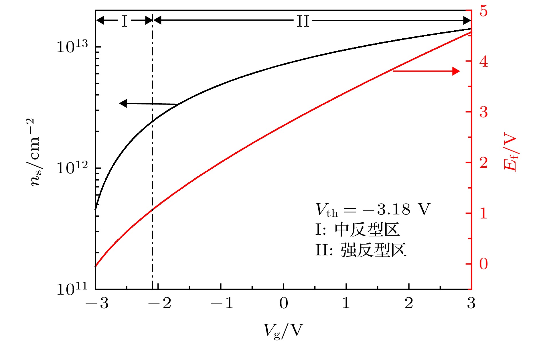
    图 6  Vg与2DEG浓度nsEf的关系曲线

    Figure 6.  The curve of the density ns of 2DEG and Ef versus Vg

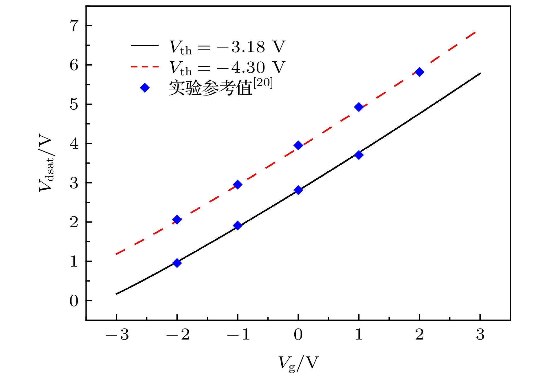
    图 7  VgVdsat的关系曲线

    Figure 7.  The curve of Vdsat versus Vg.

    图 8  传统模型和本文模型得到的VdsCofd的关系曲线

    Figure 8.  The curve of Cofd versus Vds obtained from the traditional model and the model in this paper.

    图 9  VthCofd的影响关系曲线(插图为Vth与Al组分x和掺杂浓度ND的关系曲线)

    Figure 9.  The curve ofCofd versus Vth(The illustration show the curve of Vth with Al component and doped concentration).

    图 10  温度TCofd的影响关系曲线

    Figure 10.  The curve of Cofd versus T

    图 11  不同漏极偏压下Cofd对温度敏感程度的关系曲线

    Figure 11.  The curve oftemperature sensitivity of Cofd under different drain bias.

    表 1  模型仿真的器件参数值

    Table 1.  Model parameters in this paper.

    参数定义数值
    εx有效介电常数7.65ε0
    Esat/V·μm–1饱和电场15
    Ld/μm漏端沟道长度1
    Tg/μm栅极厚度0.3
    TAlGaN/nmAlGaN层厚度22
    EAINg/eVAIN禁带宽度6.13
    EGaNg/eVGaN禁带宽度3.42
    VtempVth的依赖系数温度0.1689
    TNOM/K器件温标300
    ξ1拟合参数1.1
    ξ2拟合参数0.24
    m拟合参数1.2
    p拟合参数0.307
    τ拟合参数3.2
    a拟合参数1.497
    b拟合参数1.9
    c拟合参数0.31
    DownLoad: CSV
  • [1]

    Jones E A, Wang F F, Costinett D 2016 IEEE J. Emerg. Sel. Top. Power Electron. 4 707Google Scholar

    [2]

    王林, 胡伟达, 陈效双, 陆卫 2010 物理学报 59 5730Google Scholar

    Wang L, Hu W D, Chen X S, Lu W 2010 Acta Phys. Sin. 59 5730Google Scholar

    [3]

    Zhang A, Zhang L, Tang Z, Cheng X, Wang Y, Chen K J, Chan M 2014 IEEE Trans. Electron Devices 61 755Google Scholar

    [4]

    Pregaldiny F, Lallement C, Mathiot D 2002 Solid-State Electron. 46 2191Google Scholar

    [5]

    Bansal A, Paul B C, Roy K 2005 IEEE Trans. Electron Devices 52 256Google Scholar

    [6]

    Li K, Rakheja S 2018 Device Research Conference-Conference Digest, DRC the University of California, Santa Barbara, June 24–27, 2018 p1

    [7]

    Jia Y, Xu Y, Wen Z, Wu Y, Guo Y 2019 IEEE Trans. Electron Devices 66 357Google Scholar

    [8]

    Vetury R, Zhang N Q, Keller S, Mishra U K 2001 IEEE Trans. Electron Devices 48 560Google Scholar

    [9]

    郭伟玲, 陈艳芳, 李松宇, 雷亮, 柏常青 2017 发光学报 38 1000

    Guo Y L, Chen Y F, Li S Y, Lei L, Bai C Q 2017 Chin. J. Lumin. 38 1000

    [10]

    Cheng X, Wang Y 2011 IEEE Trans. Electron Devices 58 448Google Scholar

    [11]

    Dasgupta N, DasGupta A 1993 Solid-State Electron. 36 201Google Scholar

    [12]

    Huque M A, Eliza S A, Ragman T, Huq H F, Islam S K 2009 Solid-State Electron. 53 341

    [13]

    Ahsan S A, Ghosh S, Sharma K, Dasgupta A, Khandelwal S, Chauhan Y S 2016 IEEE Trans. Electron Devices 63 565

    [14]

    Rashmi, Kranti A, Haldar S, Gupta R S 2002 Solid-State Electron. 46 621Google Scholar

    [15]

    Ambacher O, Smart J, Shealy J R, Weimann N G, Chu K, Murphy M, Schaff W J, Eastman L F, Dimitrov R, Wittmer L, Stutzmann M, Rieger W, Hilsenbeck J 1999 J. Appl. Phys 85 3222Google Scholar

    [16]

    范隆, 郝跃 2007 物理学报 56 3393Google Scholar

    Fan L, Hao Y 2007 Acta Phys. Sin. 56 3393Google Scholar

    [17]

    Ambacher O, Majewski J, Miskys C, Link A, Hermann M, Eickhoff M, Stutzmann M, Bernardini F, Fiorentini V, Tilak V, Schaff B, Eastman L F 2002 J. Phys.-Condes. Matter 14 3399Google Scholar

    [18]

    Khandelwal S, Chauhan Y S, Fjeldly T A 2012 IEEE Trans. Electron Devices 59 2856Google Scholar

    [19]

    He X G, Zhao D G, Jiang D S 2015 Chin. Phys. B 24 067301Google Scholar

    [20]

    Li M, Wang Y 2008 IEEE Trans. Electron Devices 55 261Google Scholar

    [21]

    Alim M A, Rezazadeh A A, Gaquiere C 2016 Semicond. Sci. Technol. 31 125016Google Scholar

  • [1] Wang Shuai, Ge Chen, Xu Zu-Yin, Cheng Ai-Qiang, Chen Dun-Jun. Modeling of temperature effect on DC characteristics of microwave GaN devices. Acta Physica Sinica, 2024, 73(17): 177101. doi: 10.7498/aps.73.20240765
    [2] Zhang Lin, Ma Lin-Dong, Du Lin, Li Yan-Bo, Xu Xian-Feng, Huang Xin-Rong. Transient characteristics simulation of total ionizing dose effect on Si n-metal-oxide-semiconductor field effect transistor under different gate voltage. Acta Physica Sinica, 2023, 72(13): 138501. doi: 10.7498/aps.72.20230207
    [3] Xie Tian-Ci, Zhang Bin, He Bo, Li Hao-Peng, Qin Zhuang, Qian Jin-Qian, Shi Qie-Ming, Lewis Elfed, Sun Wei-Min. Mathematical algorithm model of absolute dose in radiotherapy. Acta Physica Sinica, 2021, 70(1): 018701. doi: 10.7498/aps.70.20200986
    [4] Liu Jia-Wen, Yao Ruo-He, Liu Yu-Rong, Geng Kui-Wei. A physical model of cylindrical surrounding double-gate metal-oxide-semiconductor field-effect transistor. Acta Physica Sinica, 2021, 70(15): 157302. doi: 10.7498/aps.70.20202156
    [5] Liu Nai-Zhang, Yao Ruo-He, Geng Kui-Wei. Gate capacitance model of AlGaN/GaN high electron mobility transistor. Acta Physica Sinica, 2021, 70(21): 217301. doi: 10.7498/aps.70.20210700
    [6] Ma Ji-Gang, Ma Xiao-Hua, Zhang Hui-Long, Cao Meng-Yi, Zhang Kai, Li Wen-Wen, Guo Xing, Liao Xue-Yang, Chen Wei-Wei, Hao Yue. A semiempirical model for kink effect on the AlGaN/GaN high electron mobility transistor. Acta Physica Sinica, 2012, 61(4): 047301. doi: 10.7498/aps.61.047301
    [7] Duan Bao-Xing, Yang Yin-Tang, Kevin J. Chen. Breakdown voltage analysis for new Al0.25Ga0.75N/GaN HEMT with F ion implantation. Acta Physica Sinica, 2012, 61(22): 227302. doi: 10.7498/aps.61.227302
    [8] Jiang Zhi-Hong, Wang Hui, Gao Chao. A evolving network model generated by random walk and policy attachment. Acta Physica Sinica, 2011, 60(5): 058903. doi: 10.7498/aps.60.058903
    [9] Wu Hua-Ying, Zhang He-Ming, Song Jian-Jun, Hu Hui-Yong. An model of tunneling gate current for uniaxially strained Si nMOSFET. Acta Physica Sinica, 2011, 60(9): 097302. doi: 10.7498/aps.60.097302
    [10] Li Bin, Liu Hong-Xia, Yuan Bo, Li Jin, Lu Feng-Ming. Model of electron mobility in inversion layer of strained Si/Si1-xGex n type metal-oxide-semiconductor field-effect transistors. Acta Physica Sinica, 2011, 60(1): 017202. doi: 10.7498/aps.60.017202
    [11] Wang Xin-Hua, Zhao Miao, Liu Xin-Yu, Pu Yan, Zheng Ying-Kui, Wei Ke. The experiential fit of the capacitance-voltage characteristicsof the AlGaN/AlN/GaN high electron mobility transistors. Acta Physica Sinica, 2011, 60(4): 047101. doi: 10.7498/aps.60.047101
    [12] Wang Xin-Hua, Pang Lei, Chen Xiao-Juan, Yuan Ting-Ting, Luo Wei-Jun, Zheng Ying-Kui, Wei Ke, Liu Xin-Yu. Investigation on trap by the gate fringecapacitance in GaN HEMT. Acta Physica Sinica, 2011, 60(9): 097101. doi: 10.7498/aps.60.097101
    [13] Li Qi, Zhang Bo, Li Zhao-Ji. A new analytical model of breakdown voltage for the SD LDMOS. Acta Physica Sinica, 2008, 57(3): 1891-1896. doi: 10.7498/aps.57.1891
    [14] Zhang He-Ming, Cui Xiao-Ying, Hu Hui-Yong, Dai Xian-Ying, Xuan Rong-Xi. Study on threshold voltage model of strained SiGe quantum well channel SOI PMOSFET. Acta Physica Sinica, 2007, 56(6): 3504-3508. doi: 10.7498/aps.56.3504
    [15] Fan Long, Hao Yue. The effect of radiation induced strain relaxation on electric performance of AlmGa1-mN/GaN HEMT. Acta Physica Sinica, 2007, 56(6): 3393-3399. doi: 10.7498/aps.56.3393
    [16] Guo Liang-Liang, Feng Qian, Hao Yue, Yang Yan. Study of high breakdown-voltage AlGaN/GaN FP-HEMT. Acta Physica Sinica, 2007, 56(5): 2895-2899. doi: 10.7498/aps.56.2895
    [17] Hao Yue, Han Xin-Wei, Zhang Jin-Cheng, Zhang Jin-Feng. Current slump mechanism and its physical model of AlGaN/GaN HEMTs under DC bias. Acta Physica Sinica, 2006, 55(7): 3622-3628. doi: 10.7498/aps.55.3622
    [18] Li Dong-Lin, Zeng Yi-Ping. Theoretical analysis about the influence of channel layer thickness on the 2D electron gas and its distribution in InP-based high-electron-mobility transistors. Acta Physica Sinica, 2006, 55(7): 3677-3682. doi: 10.7498/aps.55.3677
    [19] Ma Zhong-Fa, Zhuang Yi-Qi, Du Lei, Bao Jun-Lin, Li Wei-Hua. A physical-based percolation model for gate oxide TDDB. Acta Physica Sinica, 2003, 52(8): 2046-2051. doi: 10.7498/aps.52.2046
    [20] Lü Hong-Liang, Zhang Yi-Men, Zhang Yu-Ming. The simulation study of the tunneling effect in the breakdown of 4H-SiC pn junc tion diode. Acta Physica Sinica, 2003, 52(10): 2541-2546. doi: 10.7498/aps.52.2541
Metrics
  • Abstract views:  9486
  • PDF Downloads:  185
Publishing process
  • Received Date:  20 December 2019
  • Accepted Date:  31 January 2020
  • Published Online:  05 April 2020

/

返回文章
返回