-
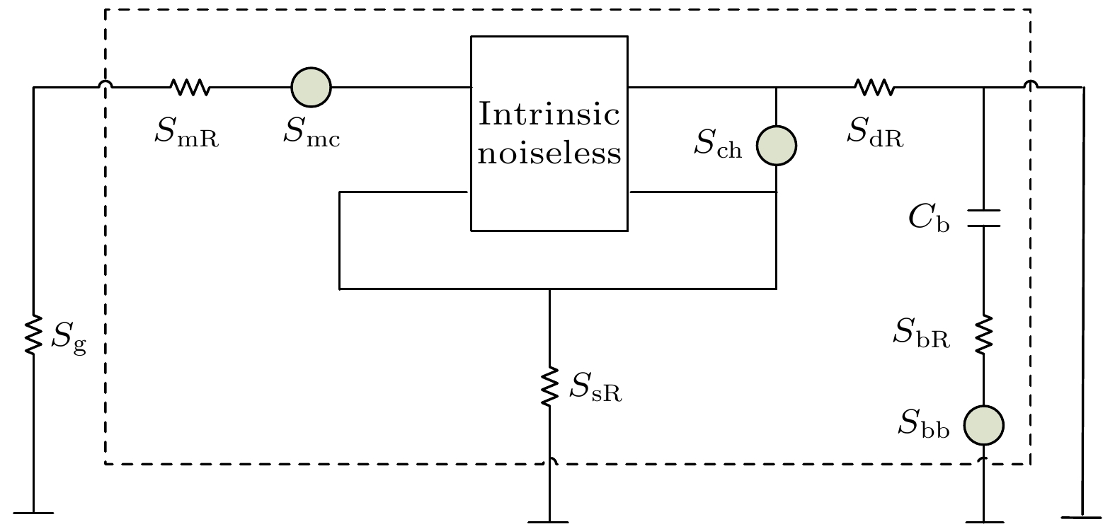
Small size metal-oxide-semiconductor field effect transistor (MOSFET), owing to their high theoretical efficiency and low production cost, have received much attention and are at the frontier of transistors. At present, their development is bottlenecked by physical limits due to equal scaling down of devices, which requires further improvement in terms of materials choice and device fabrication. As the MOSFET devices scale down to nanometer scale, on the one hand, the resulting short channel effect affects severely the thermal noise property; on the other hand, it makes the ratio of thermal noise in the gate, source, drain and substrate regions become higher and higher. However, the traditional thermal noise model mainly considers thermal noise of large-size devices, and its model does not consider the channel saturation region. In view of this, it is necessary to establish a small size MOSFET thermal noise model and analyze its characteristics. At present, there are some researches on MOSFET thermal noise, but they mainly focus on the thermal noise in channel region of large size nanoscale MOSFET. In the present work, according to the device structure and inherent thermal noise characteristics, we establish a thermal noise model for MOSFETs of 10 nm feature size. The model includes contributions of substrate region, gate-source-drain region, and channel region. In the channel region is also included the thermal noise related to the device saturation regime. Using such a model, the dependence of channel thermal noise and total thermal noise on the device bias condition and device parameters are investigated, evidencing the existence of thermal noise in the device saturation regime, which are consistent with the experimental results in the literature. The thermal noise increases with the gate voltage and source-drain voltage rising as the device structure shrinks. In a temperature range of 100–400 K, the thermal noise is basically on the order of 1021, indicating that the temperature has a great influence on the thermal noise. The thermal noise model established in this work can be applied to analyzing the noise performances of small size MOSFET devices, and the conclusions drawn from the present study are beneficial to improving the efficiency, lifetime, and response speed of MOSFETs on a nanometer scale. -
Keywords:
- thermal noise /
- nano-metal-oxide-semiconductor field effect transistor /
- short channel effect /
- device efficiency
[1] Navid R, Dutton R W 2002 Simul. Semicond. Processes Dev. 2 75
 Google Scholar
[2] Panda S, Maji B, Mukhopadhyay A K 2012 Int. J. Emerg. Technol. Adv. Eng. 12 107
 Google Scholar
[3] Liu W, Padovani A, Larcher L, Raghavan N 2014 IEEE Electron Dev. Lett. 35 157
 Google Scholar
[4] Koyama M 2015 Ph. D. Dissertation (Tokyo: Tokyo Institute of Technology
[5] Zhang Y Q, Sun Q 1993 Noise in Semiconductor Devices and Its Low Noise Technology (Beijing: National Defense Industry Press) p38 [庄奕琪, 孙青 1993 半导体器件中的噪声及其低噪声化技术(北京: 国防工业出版社)第38页
Zhang Y Q, Sun Q 1993 Noise in Semiconductor Devices and Its Low Noise Technology (Beijing: National Defense Industry Press) p38 [6] Dabhi C K, Dasgupta A, Pragya K, Harshit A, Chenming H, Yogesh S C 2018 IEEE Microw. Wirel. Co. 28 597
 Google Scholar
[7] Myeong I, Kim J, Ko H 2020 IEEE T. Comput. Aid. D 39 4351
 Google Scholar
[8] Kenji O, Shuhei A 2021 IEEE T. Electron Dev. 68 1478
 Google Scholar
[9] Schmid M, Bhogaraju S K, Hanss A, Elger G 2021 IEEE T. Instrum. Meas. 70 6500409
 Google Scholar
[10] Navid R, Jungemann C, Lee T, Thomas H, Robert W 2007 J. Appl. Phys. 101 124501
 Google Scholar
[11] Mahajan V M, Patalay P R, Jindal R P 2012 IEEE T. Electron Dev. 59 197
 Google Scholar
[12] 张梦, 姚若河, 刘玉荣 2020 物理学报 69 057101
 Google Scholar
Zhang M, Yao R K, Liu Y R 2020 Acta Phys. Sin. 69 057101
 Google Scholar
[13] Chen X , Elgabra H, Chen C H, Baugh J, Wei L 2021 IEEE ISCAS 5 22
 Google Scholar
[14] 王军, 王林, 王丹丹 2016 物理学报 23 237102
 Google Scholar
Wang J, Wang L, Wang D D 2016 Acta Phys. Sin. 23 237102
 Google Scholar
[15] Pahim V C, Galup-Montoro C, Schneider M C 2022 Nanotech 3 876
[16] Jeon J, Lee J, Kim J, Park C H, Shin H 2009 Symposium on VLSI Technology Kyoto, Japan, June 15–17, 2009 p48
[17] Knoblinger G, Klein P, Tiebout M 2001 IEEE J. Solid St. Circ. 36 831
 Google Scholar
[18] Ji Y, Nan L, Mouthaan K 2009 Asia Pacific Microwave Conference, Singapore, December 7–10, 2009 p1659
[19] Ong S. N, Yeo K S, Chew K W, Chan L H K, Boon C C International Symposium on Integrated Circuits and Systems, Paris, France, February 2–4, 2010 p306
[20] Rahman A, Lundstrom M 2002 IEEE T. Electron Dev. 49 481
 Google Scholar
[21] Andersson S, Svensson C 2005 Electron Lett. 41 869
 Google Scholar
[22] Jeon J, Lee D, Park B, Shin H 2007 Solid State Electron. 51 1034
 Google Scholar
[23] Paim V C, Galup-Montoro C, Schneider M C 2006 NSTI Nanotech. 3 876
[24] Roy A S, Enz C C 2005 IEEE T. Electron Dev. 52 611
 Google Scholar
[25] Chen C H, Chen D, Lee R, Lei P, Wan D IEEE Custom Integrated Circuits Conference San Jose, CA, USA, November 11, 2013 p6658426
-
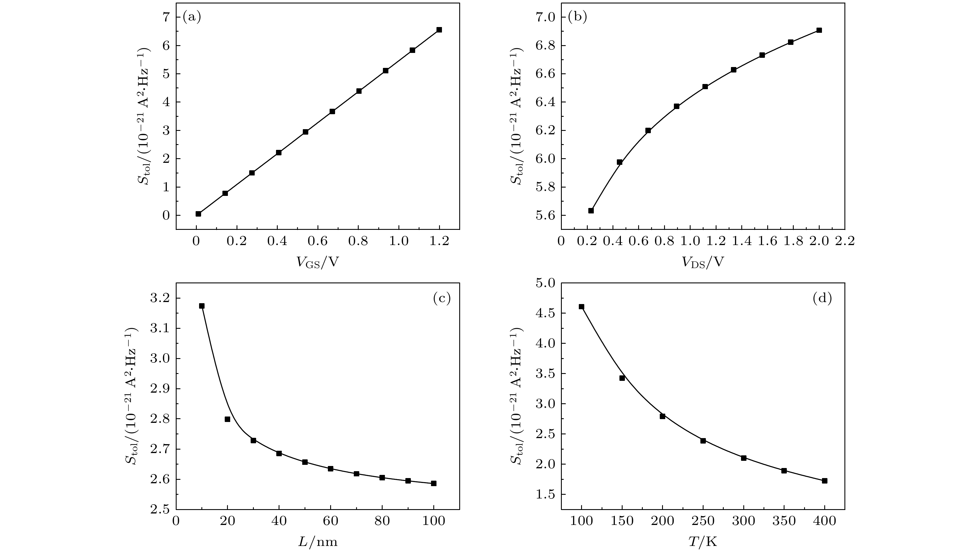
图 3 沟道热噪声与器件结构和偏置参量的关系 (a)沟道热噪声与栅极电压关系图; (b)沟道热噪声与源漏电压关系图; (c)沟道热噪声与沟道长度关系图; (d)沟道热噪声与温度关系图
Figure 3. Relationship between channel thermal noise and device structure and bias parameters: (a) Relationship between channel thermal noise and gate voltage; (b) relationship between channel thermal noise and source-drain voltage; (c) relationship between channel thermal noise and channel length voltage; (d) relationship between channel thermal noise and temperature voltage.
图 4 总热噪声与器件结构和偏置参量的关系 (a)热噪声与栅极电压关系图; (b)热噪声与源漏电压关系图; (c)热噪声与沟道长度关系图; (d)热噪声与温度关系图
Figure 4. Relationship between total thermal noise and device structure and bias parameters: (a) Relationship between thermal noise and gate voltage; (b) relationship between thermal noise and source-drain voltage; (c) relationship between thermal noise and channel length voltage; (d) relationship between thermal noise and temperature voltage.
表 1 MOSFET沟道热噪声值
Table 1. Channel thermal noise in MOSFET.
VGS/V (0—1.2 V) VDS/V (0—2 V) L/nm (10—100 nm) T/K (100—400 K) SI, ch1 SI, ch2 SI, ch1 SI, ch2 SI, ch1 SI, ch2 SI, ch1 SI, ch2 2.00×10⁻²³ 2.50×10⁻²¹ 1.49×10⁻²² 3.02×10⁻²¹ 3.94×10⁻²² 1.22×10⁻²¹ 6.48×10⁻²² 2.62×10⁻²¹ 2.84×10⁻²² 2.61×10⁻²¹ 1.52×10⁻²¹ 3.52×10⁻²¹ 1.64×10⁻²² 8.47×10⁻²² 6.69×10⁻²² 2.52×10⁻²¹ 5.48×10⁻²² 2.72×10⁻²¹ 1.90×10⁻²¹ 3.51×10⁻²¹ 1.23×10⁻²² 6.48×10⁻²² 6.90×10⁻²² 2.42×10⁻²¹ 8.12×10⁻²² 2.83×10⁻²¹ 2.12×10⁻²¹ 3.50×10⁻²¹ 9.93×10⁻²³ 5.25×10⁻²² 7.12×10⁻²² 2.42×10⁻²¹ 1.08×10⁻²¹ 2.94×10⁻²¹ 2.26×10⁻²¹ 3.50×10⁻²¹ 8.35×10⁻²³ 4.42×10⁻²² 7.64×10⁻²² 2.41×10⁻²¹ 1.34×10⁻²¹ 3.05×10⁻²¹ 2.36×10⁻²¹ 3.49×10⁻²¹ 7.22×10⁻²³ 3.81×10⁻²² 7.86×10⁻²² 2.41×10⁻²¹ 1.60×10⁻²¹ 3.16×10⁻²¹ 2.45×10⁻²¹ 3.48×10⁻²¹ 6.36×10⁻²³ 3.35×10⁻²² 7.78×10⁻²² 2.40×10⁻²¹ 1.87×10⁻²¹ 3.27×10⁻²¹ 2.51×10⁻²¹ 3.48×10⁻²¹ 5.69×10⁻²³ 2.99×10⁻²² 7.76×10⁻²² 2.40×10⁻²¹ 2.13×10⁻²¹ 3.38×10⁻²¹ 2.56×10⁻²¹ 3.47×10⁻²¹ 5.14×10⁻²³ 2.70×10⁻²² 7.74×10⁻²² 2.39×10⁻²¹ 2.40×10⁻²¹ 3.49×10⁻²¹ 2.61×10⁻²¹ 3.47×10⁻²¹ 4.69×10⁻²³ 2.46×10⁻²² 7.72×10⁻²² 2.37×10⁻²¹ -
[1] Navid R, Dutton R W 2002 Simul. Semicond. Processes Dev. 2 75
 Google Scholar
[2] Panda S, Maji B, Mukhopadhyay A K 2012 Int. J. Emerg. Technol. Adv. Eng. 12 107
 Google Scholar
[3] Liu W, Padovani A, Larcher L, Raghavan N 2014 IEEE Electron Dev. Lett. 35 157
 Google Scholar
[4] Koyama M 2015 Ph. D. Dissertation (Tokyo: Tokyo Institute of Technology
[5] Zhang Y Q, Sun Q 1993 Noise in Semiconductor Devices and Its Low Noise Technology (Beijing: National Defense Industry Press) p38 [庄奕琪, 孙青 1993 半导体器件中的噪声及其低噪声化技术(北京: 国防工业出版社)第38页
Zhang Y Q, Sun Q 1993 Noise in Semiconductor Devices and Its Low Noise Technology (Beijing: National Defense Industry Press) p38 [6] Dabhi C K, Dasgupta A, Pragya K, Harshit A, Chenming H, Yogesh S C 2018 IEEE Microw. Wirel. Co. 28 597
 Google Scholar
[7] Myeong I, Kim J, Ko H 2020 IEEE T. Comput. Aid. D 39 4351
 Google Scholar
[8] Kenji O, Shuhei A 2021 IEEE T. Electron Dev. 68 1478
 Google Scholar
[9] Schmid M, Bhogaraju S K, Hanss A, Elger G 2021 IEEE T. Instrum. Meas. 70 6500409
 Google Scholar
[10] Navid R, Jungemann C, Lee T, Thomas H, Robert W 2007 J. Appl. Phys. 101 124501
 Google Scholar
[11] Mahajan V M, Patalay P R, Jindal R P 2012 IEEE T. Electron Dev. 59 197
 Google Scholar
[12] 张梦, 姚若河, 刘玉荣 2020 物理学报 69 057101
 Google Scholar
Zhang M, Yao R K, Liu Y R 2020 Acta Phys. Sin. 69 057101
 Google Scholar
[13] Chen X , Elgabra H, Chen C H, Baugh J, Wei L 2021 IEEE ISCAS 5 22
 Google Scholar
[14] 王军, 王林, 王丹丹 2016 物理学报 23 237102
 Google Scholar
Wang J, Wang L, Wang D D 2016 Acta Phys. Sin. 23 237102
 Google Scholar
[15] Pahim V C, Galup-Montoro C, Schneider M C 2022 Nanotech 3 876
[16] Jeon J, Lee J, Kim J, Park C H, Shin H 2009 Symposium on VLSI Technology Kyoto, Japan, June 15–17, 2009 p48
[17] Knoblinger G, Klein P, Tiebout M 2001 IEEE J. Solid St. Circ. 36 831
 Google Scholar
[18] Ji Y, Nan L, Mouthaan K 2009 Asia Pacific Microwave Conference, Singapore, December 7–10, 2009 p1659
[19] Ong S. N, Yeo K S, Chew K W, Chan L H K, Boon C C International Symposium on Integrated Circuits and Systems, Paris, France, February 2–4, 2010 p306
[20] Rahman A, Lundstrom M 2002 IEEE T. Electron Dev. 49 481
 Google Scholar
[21] Andersson S, Svensson C 2005 Electron Lett. 41 869
 Google Scholar
[22] Jeon J, Lee D, Park B, Shin H 2007 Solid State Electron. 51 1034
 Google Scholar
[23] Paim V C, Galup-Montoro C, Schneider M C 2006 NSTI Nanotech. 3 876
[24] Roy A S, Enz C C 2005 IEEE T. Electron Dev. 52 611
 Google Scholar
[25] Chen C H, Chen D, Lee R, Lei P, Wan D IEEE Custom Integrated Circuits Conference San Jose, CA, USA, November 11, 2013 p6658426
Catalog
Metrics
- Abstract views: 4813
- PDF Downloads: 76
- Cited By: 0


 DownLoad:


