-
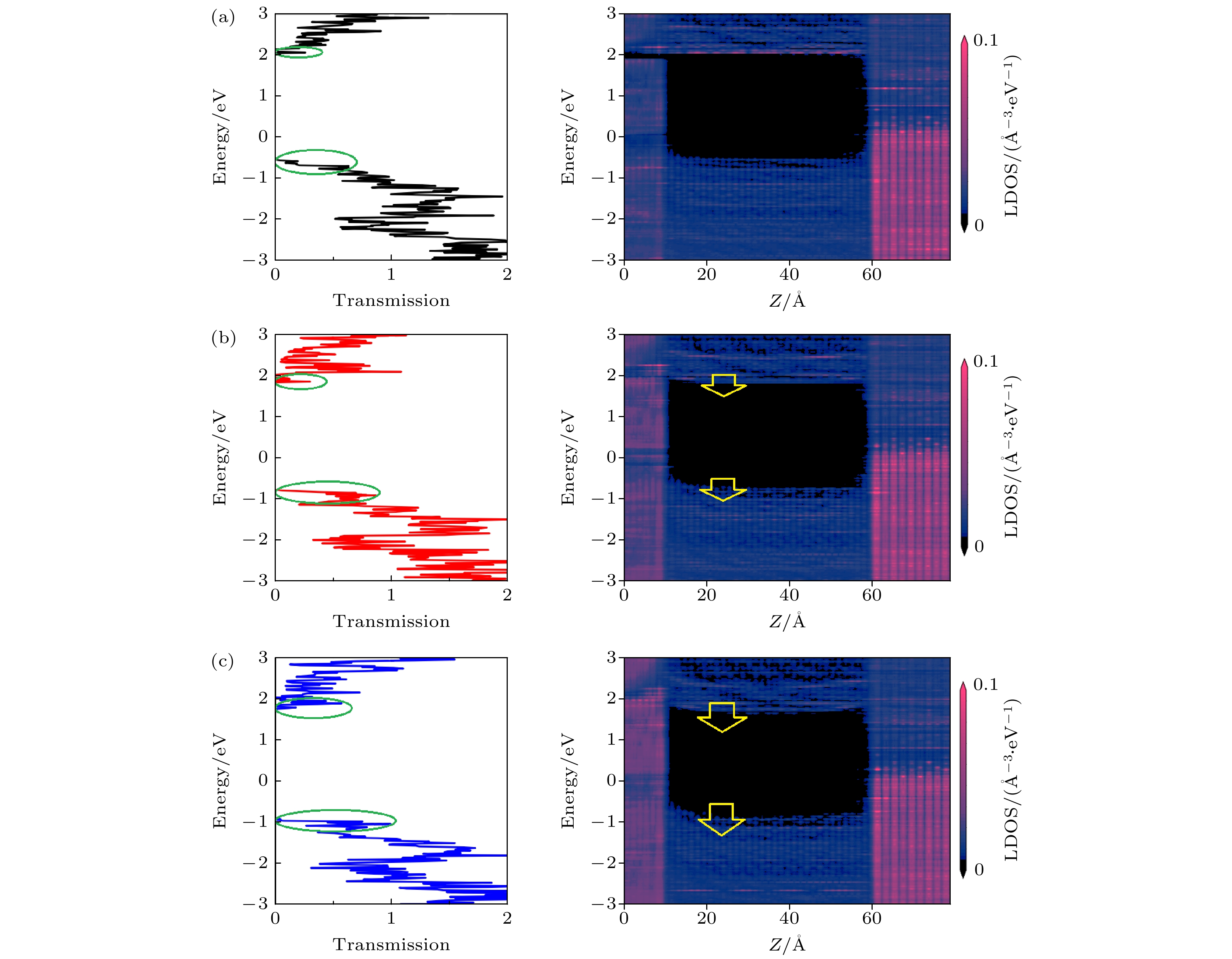
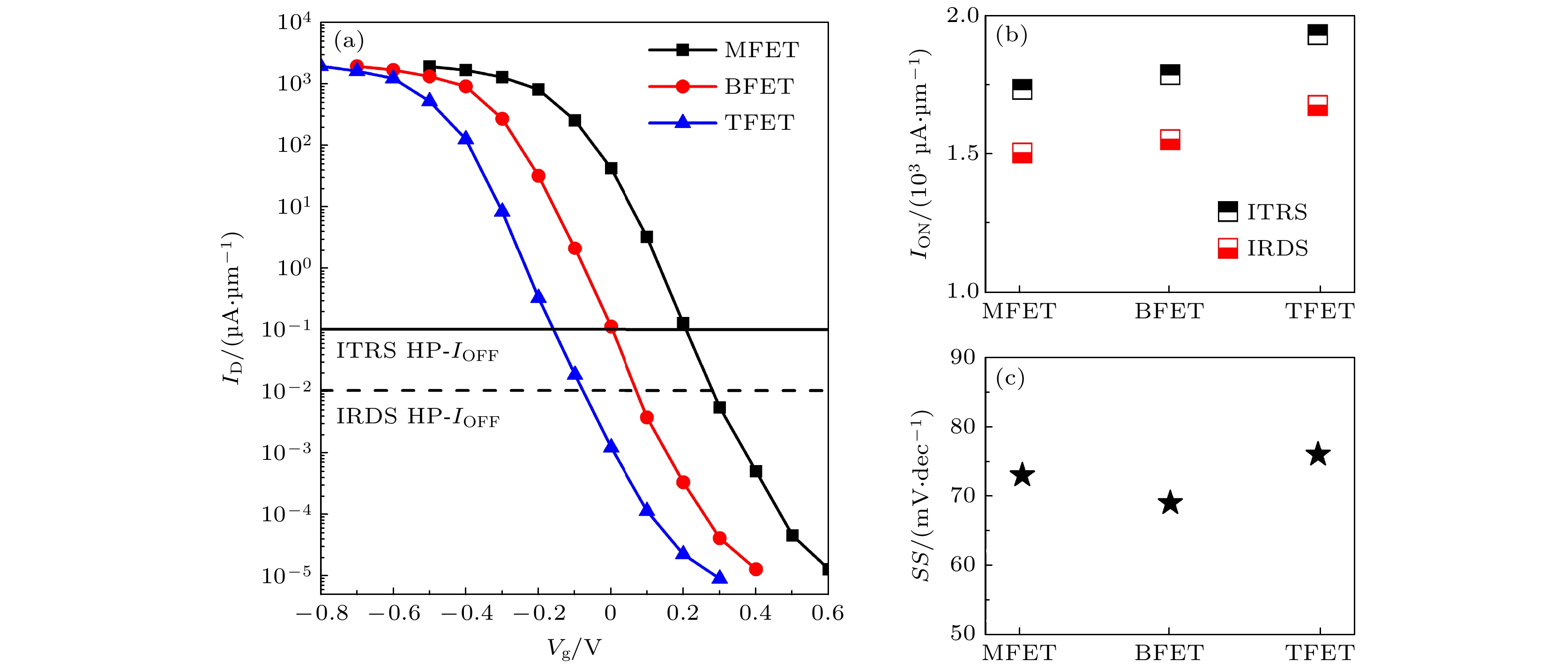
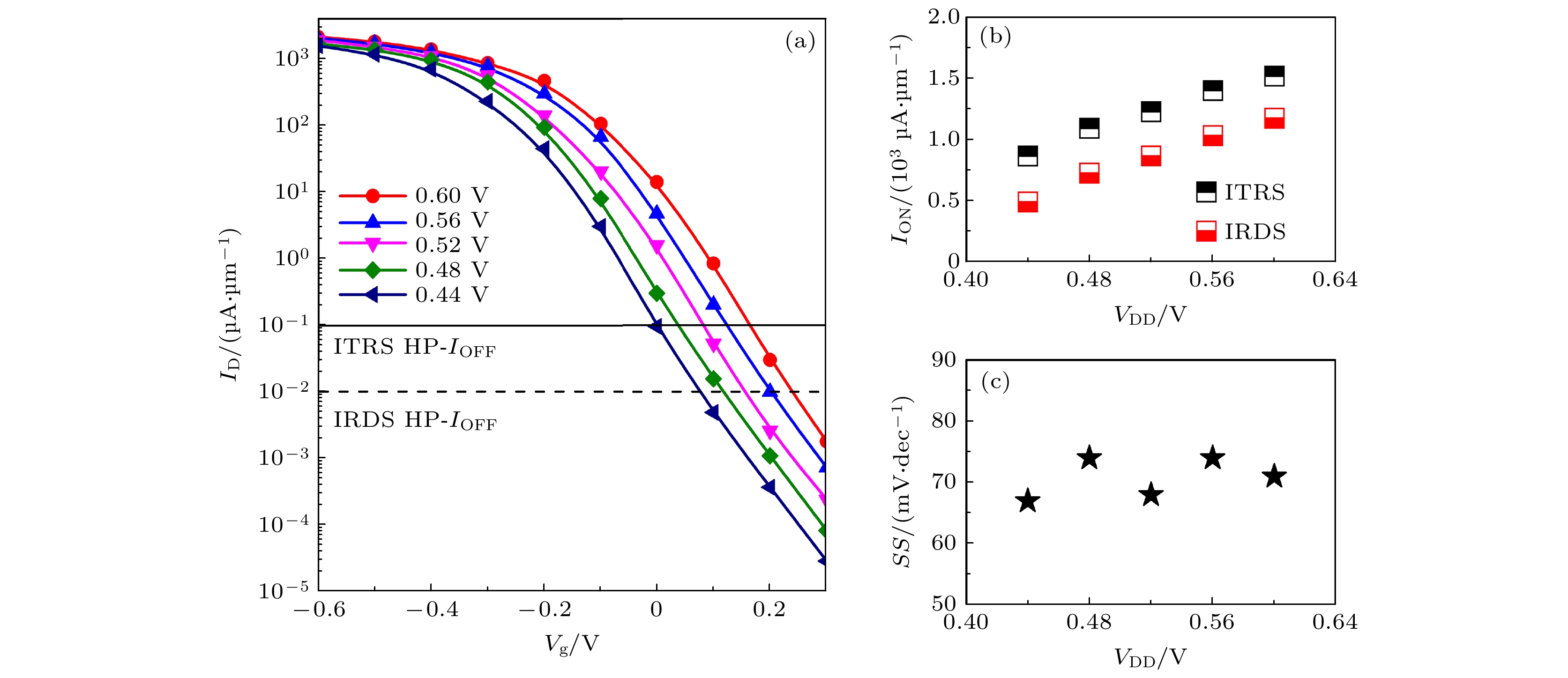
By using the first-principles method based on density functional theory and non-equilibrium Green’s function, the transport properties of 5-nm two-dimensional SiC field-effect transistors with asymmetric metal phase 1T-MoS2 sources and Pd drain electrodes are investigated. The influence mechanism of increasing the electrode layers of 1T-MoS2 and reducing the working electrical compression on the device performance is systematically analyzed. The Schottky barriers extracted from the zero bias and zero gate voltage transport spectra show that the valence band maximum of SiC in the channel regions of MFET, BFET and TFET are closer to the Fermi level after the source drain electrode has been balanced. Therefore, these three devices belong to P-type contact, and the height of the hole Schottky barrier increases with the increase of the number of 1T-MoS2 layers in the source electrode, which are 0.6, 0.76, and 0.88 eV, respectively. In addition, the increase of 1T-MoS2 layers will also lead to the increase of the density of states in the source electrode, thereby improving the transport coefficient at the band edge. The effects of the two on the transport capacity of the device are opposite, and there is a competitive relationship. The transfer characteristics of devices show that the wide band gap of SiC can significantly suppress the short channel effect, so that all devices can meet the requirements of Off-state. More importantly, the subthreshold swings of all devices at an operating voltage of 0.64 V are all close to the physical limit of 60 mV/dec. The ON-state currents of MFET, BFET and TFET can reach 1553, 1601 and 1702 μA/μm under the more stringent IRDS HP standard, and the three performance parameters, i.e. intrinsic gate capacitance, power-delay product and delay time, can greatly exceed the standards in the international road map of equipment and systems (IRDS) for high-performance devices. In addition, the working voltage of MFET can be reduced to 0.52 V, and the corresponding power-delay product and delay time are as low as 0.086 fJ/μm and 0.038 ps, which are only 14% and 4% of the IRDS standard. The asymmetric source drain electrode design strategy proposed in this work not only solves the problems about low On-state current and short channel effect restricting Off-state current of existing two-dimensional material field-effect transistors, but also provides an important solution for developing ultra-low power nano electronic devices in the post Moore era.
-
Keywords:
- two-dimensional material /
- first principles /
- field-effect transistor /
- transfer characteristic /
- short channel effect
[1] Wang Q H, Kalantar-Zadeh K, Kis A, Coleman J N, Strano M S 2012 Nat. Nanotech. 7 699
 Google Scholar
[2] 赵俊, 姚璨, 曾晖 2024 物理学报 73 126802
 Google Scholar
Zhao J, Yao C, Zeng H 2024 Acta Phys. Sin. 73 126802
 Google Scholar
[3] Cui Y, Li B, Li J B, Wei Z M 2018 Sci. China-Phys. Mech. Astron. 61 016801
 Google Scholar
[4] Wu D, Cao X H, Jia P J, et al. 2020 Sci. China-Phys. Mech. Astron. 63 276811
 Google Scholar
[5] Liu Q, Huang X D, Chen J J, Wu D, Deng X Q, Fan Z Q, Xie H Q, Chen K Q 2025 Appl. Phys. Lett. 126 253502
 Google Scholar
[6] Radisavljevic B, Radenovic A, Brivio J, Giacometti V, Kis A 2011 Nat. Nanotech. 6 147
 Google Scholar
[7] Cui Y, Zhou Z Q, Li T, Wang K Y, Li J B, Wei Z M 2019 Adv. Funct. Mater. 29 1900040
 Google Scholar
[8] Ren Y, Zhou X Y, Zhou G H 2021 Phys. Rev. B 103 045405
 Google Scholar
[9] Liu Q, Li J J, Wu D, Deng X Q, Zhang Z H, Fan Z Q, Chen K Q 2021 Phys. Rev. B 104 045412
 Google Scholar
[10] Zhou W X, Cheng Y, Chen K Q, Xie G F, Wang T, Zhang G 2020 Adv. Funct. Mater. 30 1903829
 Google Scholar
[11] Quhe R G, Wang Y Y, Lu J 2015 Chin. Phys. B 24 088105
 Google Scholar
[12] Huang X D, Liu Q, Xie H Q, Deng X Q, Fan Z Q, Wu D, Chen K Q 2023 IEEE Trans. Electron. Dev. 70 5462
 Google Scholar
[13] 郭颖, 潘峰, 姚彬彬, 孟豪, 吕劲 2024 物理学报 73 207304
 Google Scholar
Guo Y, Pan F, Yao B B, Meng H, Lü J 2024 Acta Phys. Sin. 73 207304
 Google Scholar
[14] Qu H Z, Zhang S L, Cao J, et al. 2024 Sci. Bull. 69 1427
 Google Scholar
[15] Ma L K, Tao Q Y, Chen Y, Lu Z Y, Liu L T, Li Z W, Lu D L, Wang Y L, Liao L, Liu Y 2023 Nano Lett. 23 8303
 Google Scholar
[16] Chabi S, Guler Z, Brearley A J, Benavidez A D, Luk T S 2021 Nanomaterials 11 1799
 Google Scholar
[17] Zhou B H, Zhou B L, Liu G, et al. 2016 Physica B 500 106
 Google Scholar
[18] Farokhnezhad M, Esmaeilzadeh M, Ahmadi S, Pournaghavi N 2015 J. Appl. Phys. 117 173913
 Google Scholar
[19] Cui X Q, Liu Q, Fan Z Q, Zhang Z H 2020 Org. Electron. 84 105808
 Google Scholar
[20] 邓旭良, 冀先飞, 王德君, 黄玲琴 2022 物理学报 71 058102
 Google Scholar
Deng X L, Ji X F, Wang D J, Huang L Q 2022 Acta Phys. Sin. 71 058102
 Google Scholar
[21] Xie H Q, Li J Y, Liu G, Cai X Y, Fan Z Q 2019 IEEE Trans. Electron Devices 66 5111
 Google Scholar
[22] Xie H Q, Wu D, Deng X Q, Fan Z Q, Zhou W X, Xiang C Q, Liu Y Y 2021 Chin. Phys. B 30 117102
 Google Scholar
[23] International roadmap for devices and systems (IRDS)(2023 Edition) https://irds.ieee.org
[24] Okyay A K, Chui C O, Saraswat K C 2006 Appl. Phys. Lett. 88 063506
 Google Scholar
[25] Li D W, Zhao M, Liang K, et al. 2020 Nanoscal 12 21610
 Google Scholar
[26] Wu J Y, Chun Y T, Li S P, Zhang T, Chu D P 2018 ACS Appl. Mater. Interfaces 10 24613
 Google Scholar
[27] Liu Z, Cao G, Guan Z Z, Tian Y, Liu J D, Chen J, Deng S Z, Liu F 2024 J. Mater. Chem. C 12 17395
 Google Scholar
[28] Smidstrup S, Markussen T, Vancraeyveld P, et al. 2020 J. Phys. Condens. Matter 32 015901
 Google Scholar
[29] Büttiker M, Imry Y, Landauer R, Pinhas S 1985 Phys. Rev. B 31 6207
 Google Scholar
[30] Liu H, Neal A T, Ye P D 2012 ACS Nano 6 8563
 Google Scholar
[31] Xie H Q, Li J Y, Liu G, Cai X Y, Fan Z Q 2020 IEEE Trans. Electron Devices 67 4130
 Google Scholar
[32] Zhao P, Chauhan J, Guo J 2009 Nano Lett. 9 684
 Google Scholar
[33] Fan Z Q, Zhang Z H, Yang S Y 2020 Nanoscale 12 21750
 Google Scholar
-
表 1 MFET, BFET和TFET的性能与IRDS高性能设备要求的对比
Table 1. Performances of the MFET, BFET和TFET against the HP devices requirements of the IRDS.
Cg/
(fF·μm–1)PDP/
(fJ·μm–1)τ/ps IRDS标准 0.39 0.49 0.96 MFET (VDD = 0.64 V) 0.150 0.061 0.064 BFET (VDD = 0.64 V) 0.155 0.063 0.064 TFET (VDD = 0.64 V) 0.134 0.055 0.051 MFET (VDD = 0.60 V) 0.146 0.071 0.056 MFET (VDD = 0.56 V) 0.138 0.078 0.043 MFET (VDD = 0.52 V) 0.142 0.086 0.038 -
[1] Wang Q H, Kalantar-Zadeh K, Kis A, Coleman J N, Strano M S 2012 Nat. Nanotech. 7 699
 Google Scholar
[2] 赵俊, 姚璨, 曾晖 2024 物理学报 73 126802
 Google Scholar
Zhao J, Yao C, Zeng H 2024 Acta Phys. Sin. 73 126802
 Google Scholar
[3] Cui Y, Li B, Li J B, Wei Z M 2018 Sci. China-Phys. Mech. Astron. 61 016801
 Google Scholar
[4] Wu D, Cao X H, Jia P J, et al. 2020 Sci. China-Phys. Mech. Astron. 63 276811
 Google Scholar
[5] Liu Q, Huang X D, Chen J J, Wu D, Deng X Q, Fan Z Q, Xie H Q, Chen K Q 2025 Appl. Phys. Lett. 126 253502
 Google Scholar
[6] Radisavljevic B, Radenovic A, Brivio J, Giacometti V, Kis A 2011 Nat. Nanotech. 6 147
 Google Scholar
[7] Cui Y, Zhou Z Q, Li T, Wang K Y, Li J B, Wei Z M 2019 Adv. Funct. Mater. 29 1900040
 Google Scholar
[8] Ren Y, Zhou X Y, Zhou G H 2021 Phys. Rev. B 103 045405
 Google Scholar
[9] Liu Q, Li J J, Wu D, Deng X Q, Zhang Z H, Fan Z Q, Chen K Q 2021 Phys. Rev. B 104 045412
 Google Scholar
[10] Zhou W X, Cheng Y, Chen K Q, Xie G F, Wang T, Zhang G 2020 Adv. Funct. Mater. 30 1903829
 Google Scholar
[11] Quhe R G, Wang Y Y, Lu J 2015 Chin. Phys. B 24 088105
 Google Scholar
[12] Huang X D, Liu Q, Xie H Q, Deng X Q, Fan Z Q, Wu D, Chen K Q 2023 IEEE Trans. Electron. Dev. 70 5462
 Google Scholar
[13] 郭颖, 潘峰, 姚彬彬, 孟豪, 吕劲 2024 物理学报 73 207304
 Google Scholar
Guo Y, Pan F, Yao B B, Meng H, Lü J 2024 Acta Phys. Sin. 73 207304
 Google Scholar
[14] Qu H Z, Zhang S L, Cao J, et al. 2024 Sci. Bull. 69 1427
 Google Scholar
[15] Ma L K, Tao Q Y, Chen Y, Lu Z Y, Liu L T, Li Z W, Lu D L, Wang Y L, Liao L, Liu Y 2023 Nano Lett. 23 8303
 Google Scholar
[16] Chabi S, Guler Z, Brearley A J, Benavidez A D, Luk T S 2021 Nanomaterials 11 1799
 Google Scholar
[17] Zhou B H, Zhou B L, Liu G, et al. 2016 Physica B 500 106
 Google Scholar
[18] Farokhnezhad M, Esmaeilzadeh M, Ahmadi S, Pournaghavi N 2015 J. Appl. Phys. 117 173913
 Google Scholar
[19] Cui X Q, Liu Q, Fan Z Q, Zhang Z H 2020 Org. Electron. 84 105808
 Google Scholar
[20] 邓旭良, 冀先飞, 王德君, 黄玲琴 2022 物理学报 71 058102
 Google Scholar
Deng X L, Ji X F, Wang D J, Huang L Q 2022 Acta Phys. Sin. 71 058102
 Google Scholar
[21] Xie H Q, Li J Y, Liu G, Cai X Y, Fan Z Q 2019 IEEE Trans. Electron Devices 66 5111
 Google Scholar
[22] Xie H Q, Wu D, Deng X Q, Fan Z Q, Zhou W X, Xiang C Q, Liu Y Y 2021 Chin. Phys. B 30 117102
 Google Scholar
[23] International roadmap for devices and systems (IRDS)(2023 Edition) https://irds.ieee.org
[24] Okyay A K, Chui C O, Saraswat K C 2006 Appl. Phys. Lett. 88 063506
 Google Scholar
[25] Li D W, Zhao M, Liang K, et al. 2020 Nanoscal 12 21610
 Google Scholar
[26] Wu J Y, Chun Y T, Li S P, Zhang T, Chu D P 2018 ACS Appl. Mater. Interfaces 10 24613
 Google Scholar
[27] Liu Z, Cao G, Guan Z Z, Tian Y, Liu J D, Chen J, Deng S Z, Liu F 2024 J. Mater. Chem. C 12 17395
 Google Scholar
[28] Smidstrup S, Markussen T, Vancraeyveld P, et al. 2020 J. Phys. Condens. Matter 32 015901
 Google Scholar
[29] Büttiker M, Imry Y, Landauer R, Pinhas S 1985 Phys. Rev. B 31 6207
 Google Scholar
[30] Liu H, Neal A T, Ye P D 2012 ACS Nano 6 8563
 Google Scholar
[31] Xie H Q, Li J Y, Liu G, Cai X Y, Fan Z Q 2020 IEEE Trans. Electron Devices 67 4130
 Google Scholar
[32] Zhao P, Chauhan J, Guo J 2009 Nano Lett. 9 684
 Google Scholar
[33] Fan Z Q, Zhang Z H, Yang S Y 2020 Nanoscale 12 21750
 Google Scholar
Catalog
Metrics
- Abstract views: 1702
- PDF Downloads: 45
- Cited By: 0


 DownLoad:


