


-
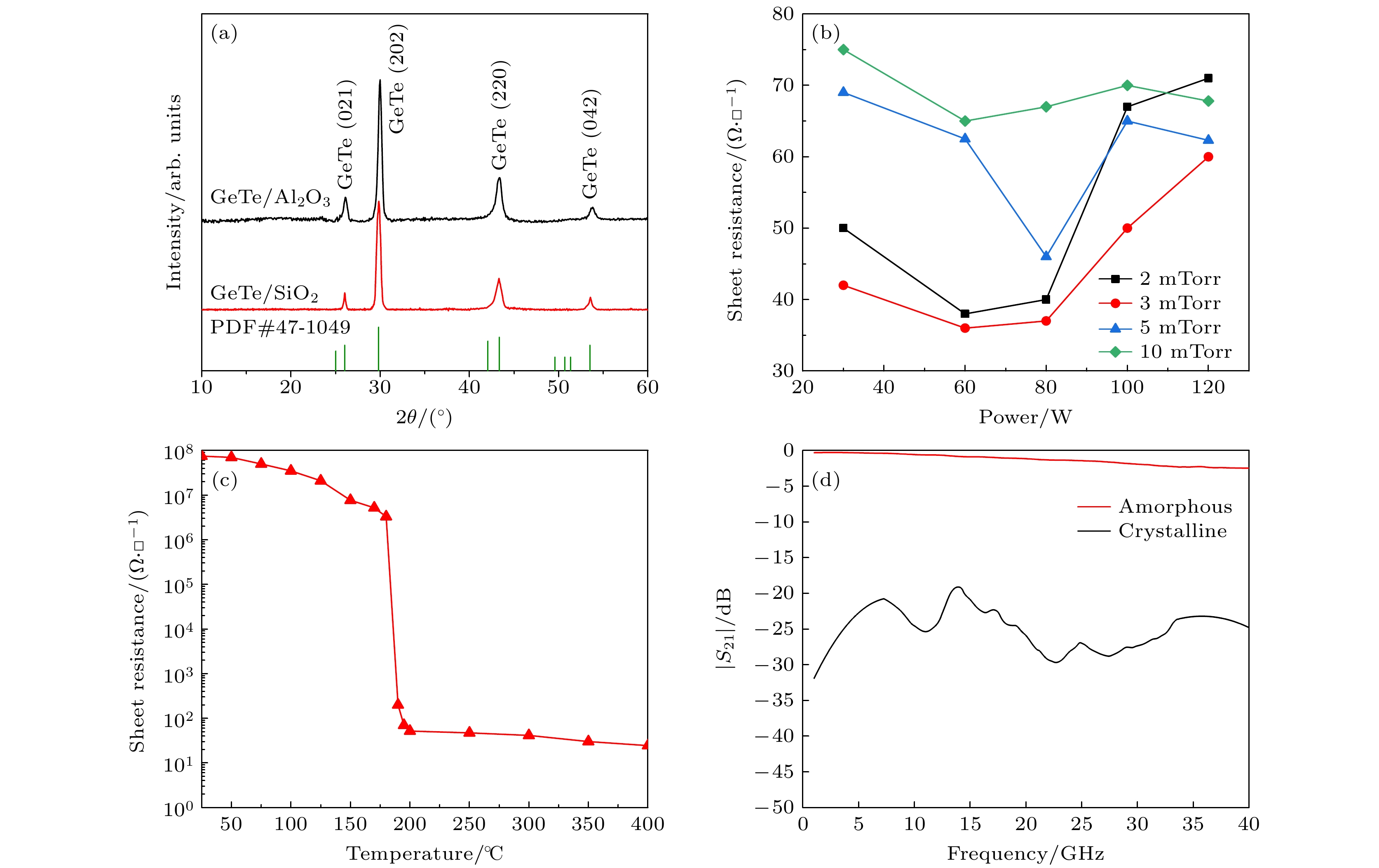
GeTe belongs to a chalcogenide phase change material, which can dynamically achieve reversible switching between the crystalline state of low resistivity and the amorphous state of high resistivity by utilizing the thermally induced phase change characteristics. The GeTe is an important functional material in the fields of memristors and nonvolatile radio frequency (RF) switches. For RF switch applications, this paper focuses on optimizing the electrical performance of GeTe thin films prepared by magnetron sputtering. By comprehensively analyzing the effects of substrate materials, sputtering conditions, and annealing conditions on the resistivity of crystalline GeTe films, effective conditions for preparing low resistivity GeTe films are explored. Fig. (a) shows that compared with the GeTe film on a SiO2 substrate, the film on an Al2O3 substrate can obtain higher crystallinity and lower resistivity. For the deposition power and pressure shown in Fig. (b), the combination of medium power (50–80 W) and low pressure (2–3 mTorr) is beneficial for low crystalline resistivity of GeTe film. Additionally, Fig. (c) shows that higher annealing temperature (350–400 ℃) can realize lower film resistivity. Finally, the experimental results show that the lowest crystalline resistivity of the prepared GeTe thin film reaches 3.6×10⁻⁶ Ω·m, and the resistance ratio is more than 106. Based on rectangular chips of GeTe film, a parallel millimeter-wave switch with zero static power is also constructed. As shown in Fig. (d), the insertion loss is less than 2.4 dB, and the isolation is greater than 19 dB in a 1–40 GHz frequency band, demonstrating the potential application of GeTe thin films in the field of broadband high-performance discrete nonvolatile RF switches.
-
Keywords:
- GeTe film /
- thermally induced phase change /
- radio frequency switch /
- discrete
[1] Rangan S, Rappaport T S, Erkip E 2014 Proc. IEEE 102 366
 Google Scholar
[2] Wu Z Y, Lu W, Bao X Y, Meng F B, Yang Z B, Sun Q, Zhao F Z, Wang Y T 2021 Int. J. Mod. Phys. B 35 15017
Google Scholar
[3] Sun P, Upadhyaya P, Jeong D, Jeong D H, Heo D, La Rue G S 2007 IEEE Microw. Wirel. Co. 17 352
Google Scholar
[4] Doan C H, Emami S, Niknejad A M, Brodersen R W 2005 IEEE J. Solid-State Circuits 40 144
Google Scholar
[5] Wolf R, Joseph A, Botula A, Slinkman J 2009 IEEE Topical Meeting on Silicon Monolithic Integrated Circuits in RF Systems San Diego, USA, January 19–21, 2009 p1
[6] Campbell C F, Dumka D C 2010 IEEE MTT-S International Microwave Symposium Anaheim, USA, May 23–28, 2010 p145
[7] Daneshmand M, Mansour R R 2011 IEEE Microw. Mag. 12 92
Google Scholar
[8] Boles T, Brogle J, Hoag D, Curcio D 2011 IEEE International Conference on Microwaves, Communications, Antennas and Electronic Systems (COMCAS 2011) Tel Aviv, Israel, November 7–9, 2011 p1
[9] Jaffe M, Abou-Khalil M, Botula A, Ellis-Monaghan J, Gambino J, Gross J, He Z X, Joseph A, Phelps R, Shank S, Slinkman J, Wolf R 2015 IEEE 15th Topical Meeting on Silicon Monolithic Integrated Circuits in RF Systems San Diego, USA, January 26–28, 2015 p30
[10] Stefanini R, Chatras M, Blondy P, Rebeiz G M 2011 IEEE MTT-S International Microwave Symposium Digest, Baltimore MD, USA, June 5–10, 2011 p1
[11] Grant P, Denhoff M, Mansour R R 2004 Proceedings of the IEEE International Conference on MEMS, NANO and Smart Systems (ICMENS) Banff, Canada, August 25–27, 2004 p515
[12] Tabata O, Tsuchiya T 2014 Reliability of MEMS: Testing of Materials and Devices (Hoboken: John Wiley & Sons) pp124–130
[13] Pan K, Wang W, Shin E, Freeman K, Subramanyam G 2015 IEEE T. Electron Dev. 62 2959
Google Scholar
[14] Morin F J 1959 Phys. Rev. Lett. 3 34
Google Scholar
[15] Bahl S K, Chopra K L 1970 J. Appl. Phys. 41 2196
Google Scholar
[16] Raoux S, Cheng H Y, Munoz B, Jordan-Sweet J 2009 European Phase Change and Ovonic Science Symposium, 2009 p91
[17] Raoux S, Ielmini D, Wuttig M, Karpov I 2012 MRS Bull. 37 118
Google Scholar
[18] Raoux S, Cheng H Y, Caldwell M A, Wong H S P 2009 Appl. Phys. Lett. 95 071910
Google Scholar
[19] Fantini P 2020 J. Phys. D Appl. Phys. 53 283002
Google Scholar
[20] Chua K, Shi L P, Zhao R, Lim K G, Chong T C, Schlesinger T E, Bain J A 2010 Appl. Phys. Lett. 97 183506
Google Scholar
[21] Wuttig M 2005 Nat. Mater. 4 265
Google Scholar
[22] Iwasaki H, Ide Y, Harigaya M, Kageyama Y, Fujimura I 1992 J. Appl. Phys. 31 461
Google Scholar
[23] Singh T, Mansour R R 2018 IEEE MTT-S International Microwave Workshop Series on Advanced Materials and Processes for RF and THz Applications (IMWS-AMP) Ann Arbor, USA, July 16–18, 2018 p3
[24] Bettoumi I, Gall N L, Blondy P 2022 IEEE Microw. Wirel. Co 32 52
Google Scholar
[25] Cruz L D L, Ivanov T, Birdwell A G, Weil J D, Kingkeo K, Zaghloul M 2023 IEEE Electron Device Lett. 70 4178
Google Scholar
[26] Charlet I, Guerber S, Naoui A, Charbonnier B, Dupré C, Lugo-Alvarez J, Hellion C, Allain M, Podevin F, Perret E 2024 IEEE Electron Device Lett. 45 500
Google Scholar
[27] Kolobov A V, Fons P, Frenkel A I, Ankudinov A L, Tominaga J, Uruga T 2004 Nat. Mater. 3 703
Google Scholar
-
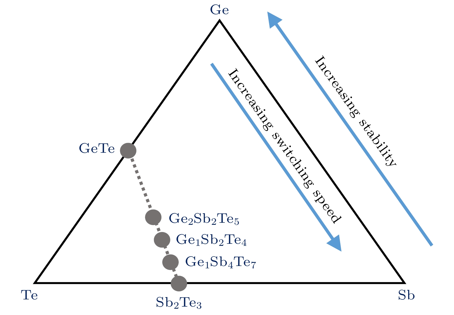
图 1 Ge-Sb-Te系统的三元相图
Figure 1. Ternary phase diagram of Ge-Sb-Te system.
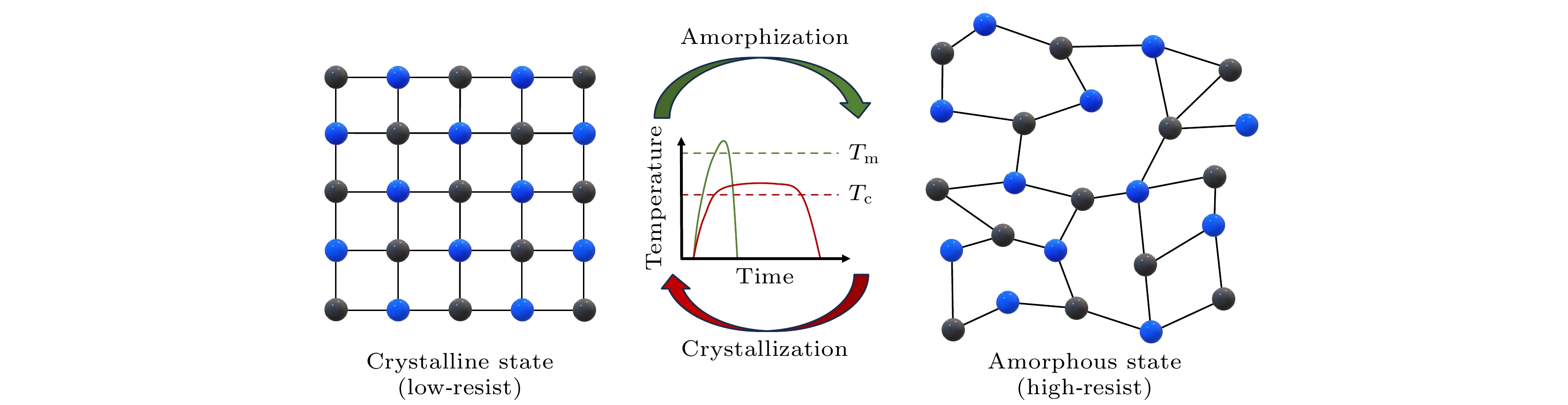
图 2 GeTe材料随温度变化的相变机制
Figure 2. Phase transition mechanism in GeTe materials with the variation of temperature.
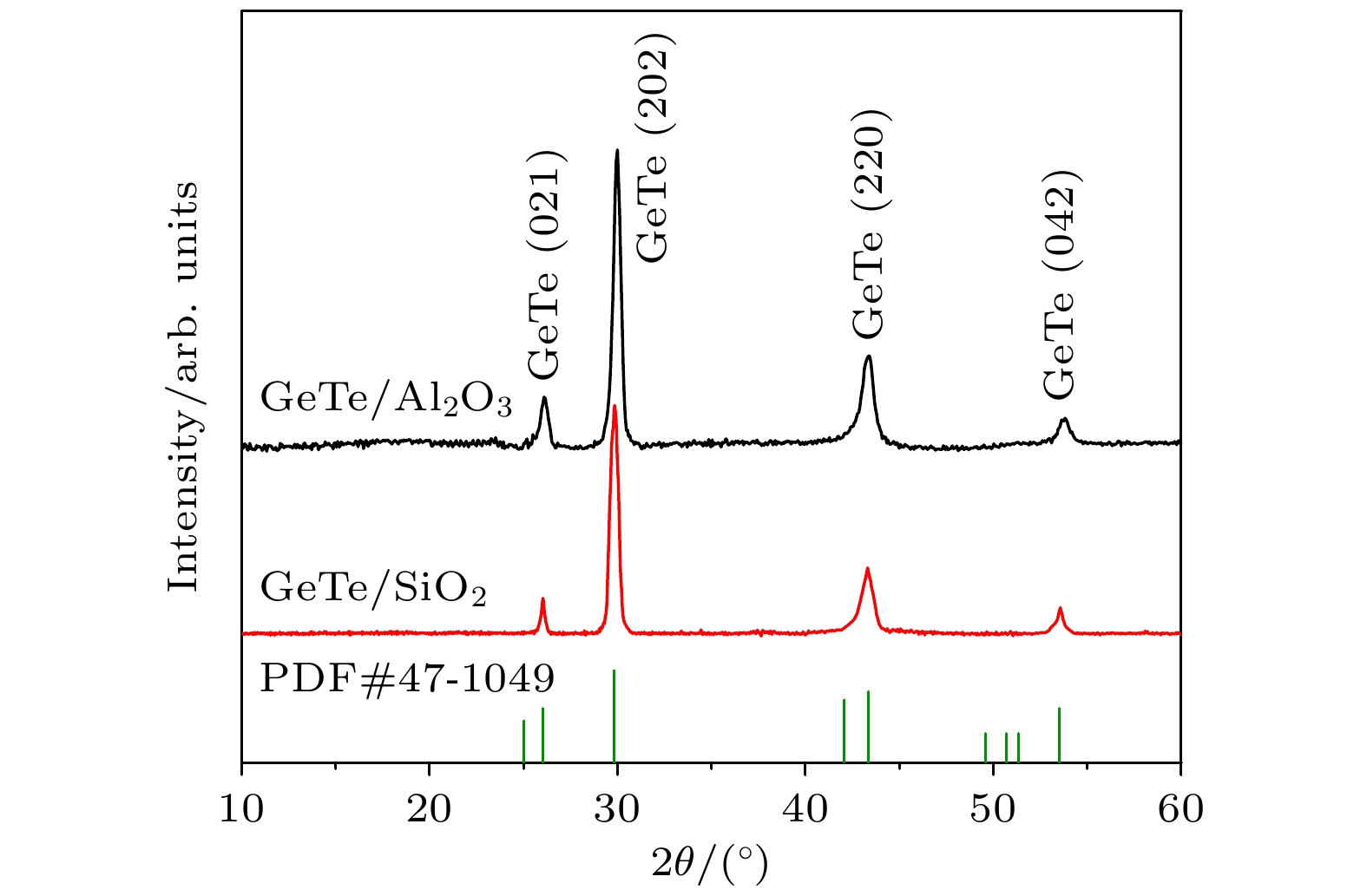
图 3 样品5和样品6的XRD图谱
Figure 3. XRD patterns of sample 5 and 6.
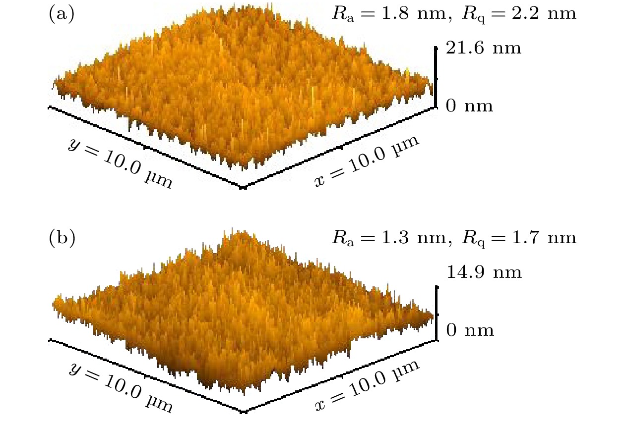
图 4 AFM三维图像 (a) 玻璃衬底; (b) 蓝宝石衬底
Figure 4. The 3D AFM patterns: (a) Glass substrate; (b) sapphire substrate.
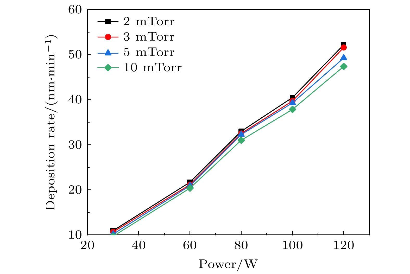
图 5 沉积条件对沉积速率的影响
Figure 5. Influence of deposition condition on the deposition rate.
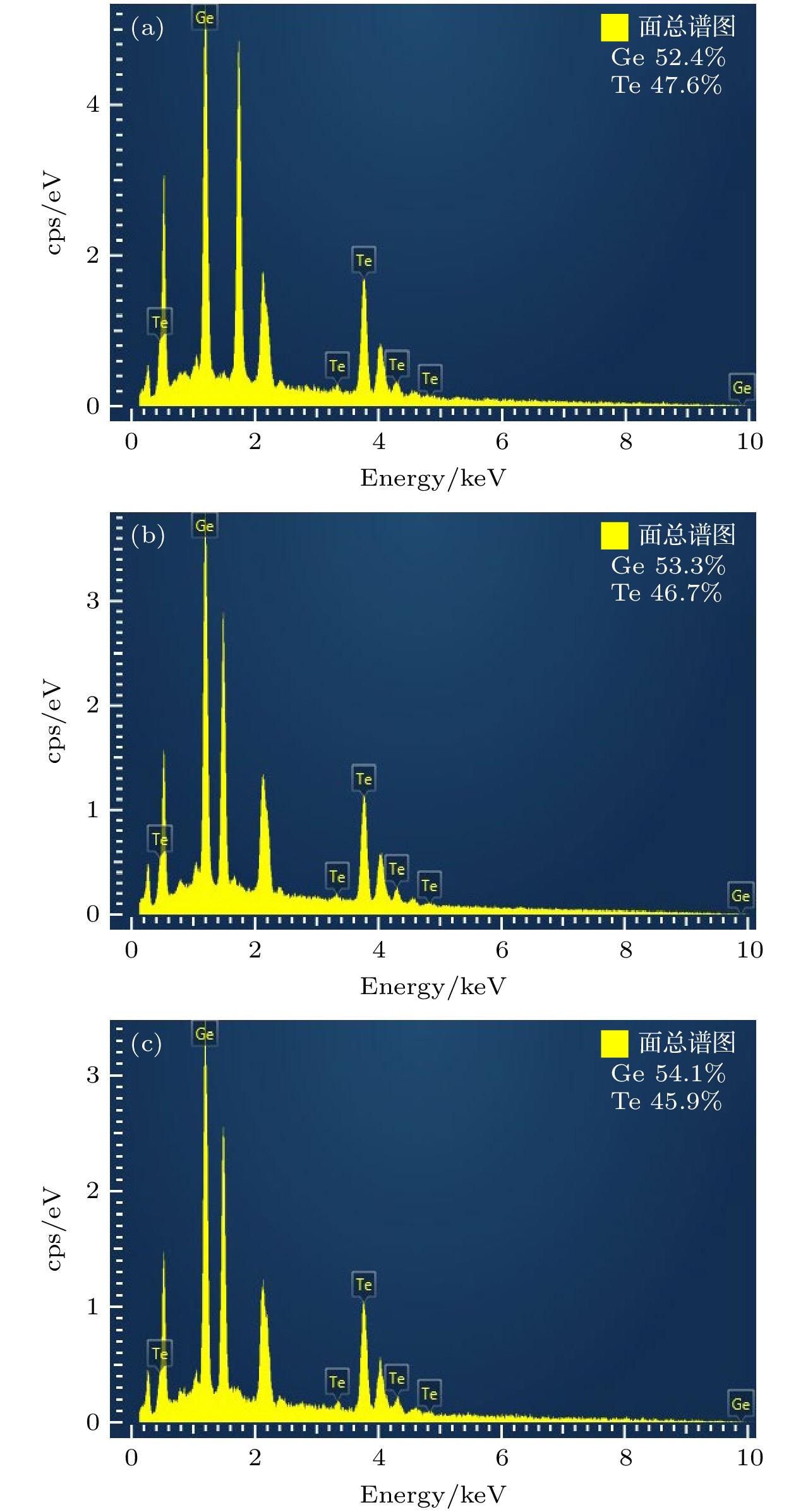
图 6 三种样品的EDS能谱分析 (a) 3 mTorr; (b) 5 mTorr; (c) 10 mTorr
Figure 6. EDS mapping for three samples: (a) 3 mTorr; (b) 5 mTorr; (c) 10 mTorr.
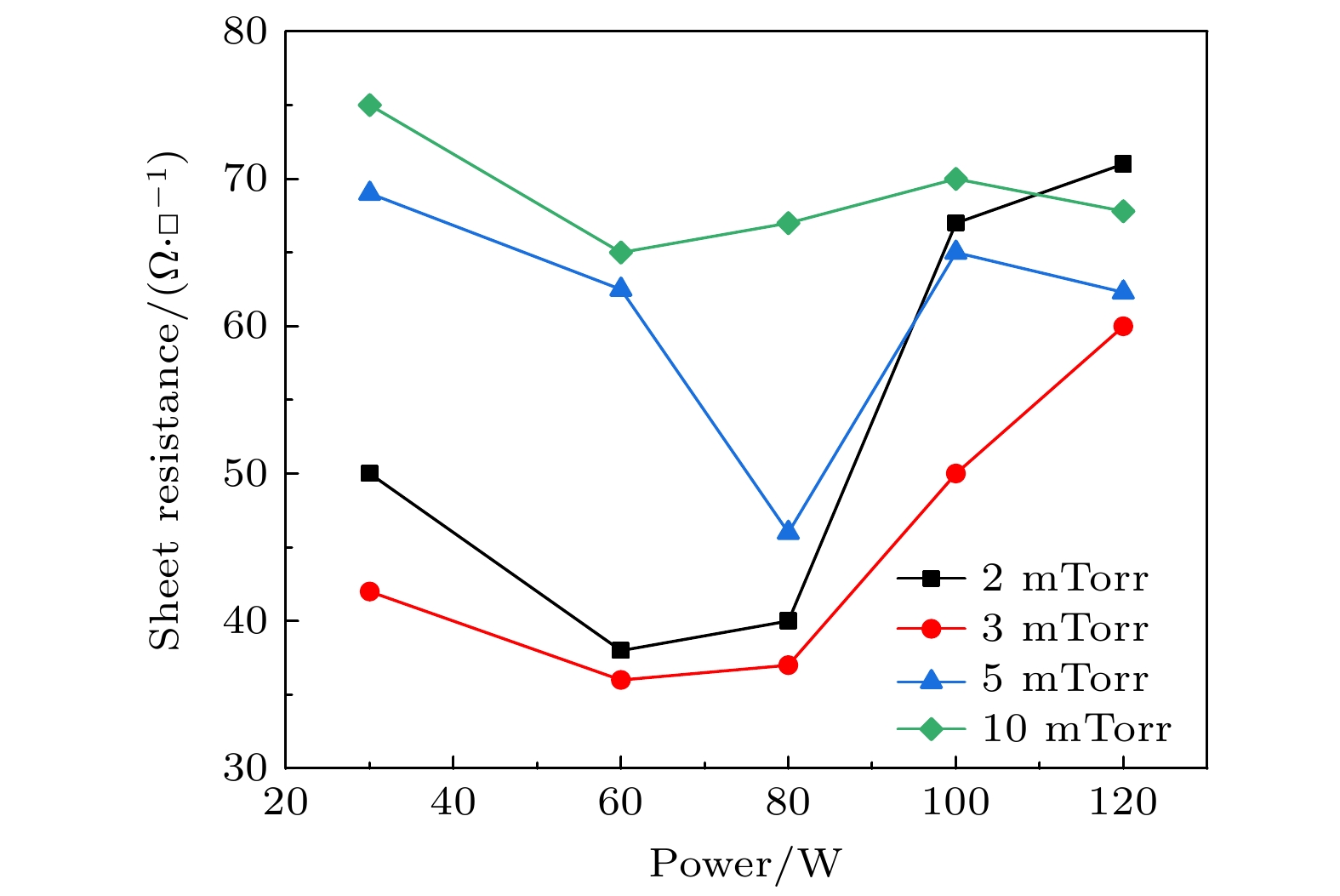
图 7 沉积条件对薄膜方阻的影响
Figure 7. Sheet resistance with the variation of deposition power and pressure.
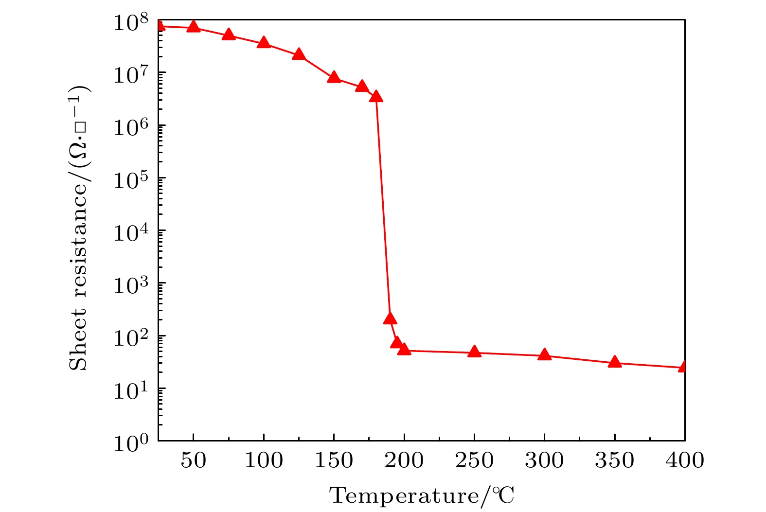
图 8 薄膜方阻随退火温度的变化
Figure 8. Sheet resistance change of GeTe samples with the variation of annealing temperature.
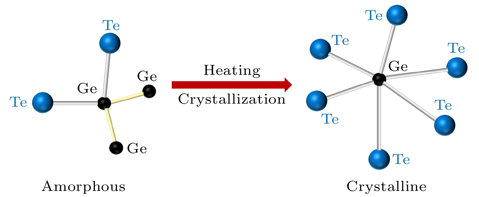
图 9 非晶态和晶态GeTe单元
Figure 9. GeTe units for the amorphous state and crystalline state.
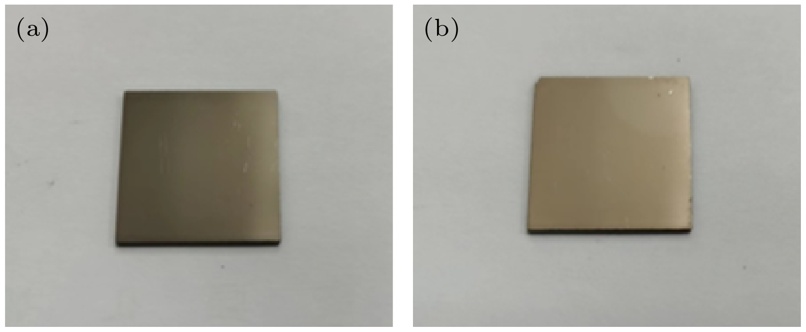
图 10 GeTe薄膜样品照片 (a) 非晶态; (b) 晶态
Figure 10. Photos of GeTe films: (a) Amorphous state; (b) crystalline state.
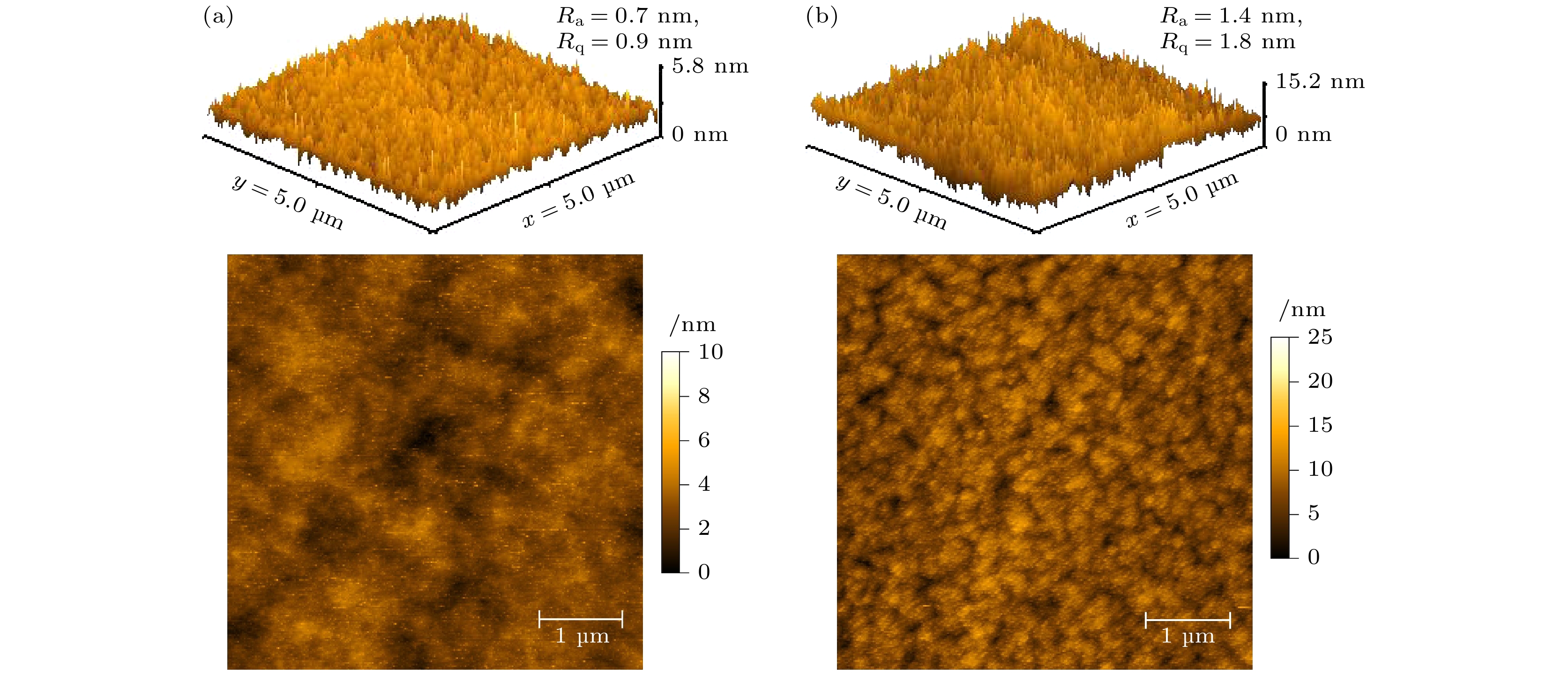
图 11 AFM图谱 (a) 非晶态; (b) 晶态
Figure 11. AFM patterns: (a) Amorphous state; (b) crystalline state.
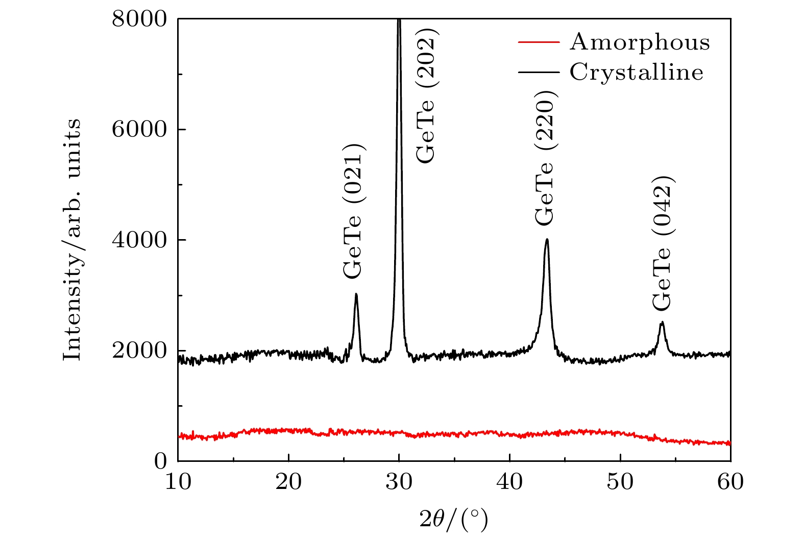
图 12 非晶态和晶态下, GeTe的XRD图谱
Figure 12. XRD patterns of GeTe film in the amorphous and crystalline states.
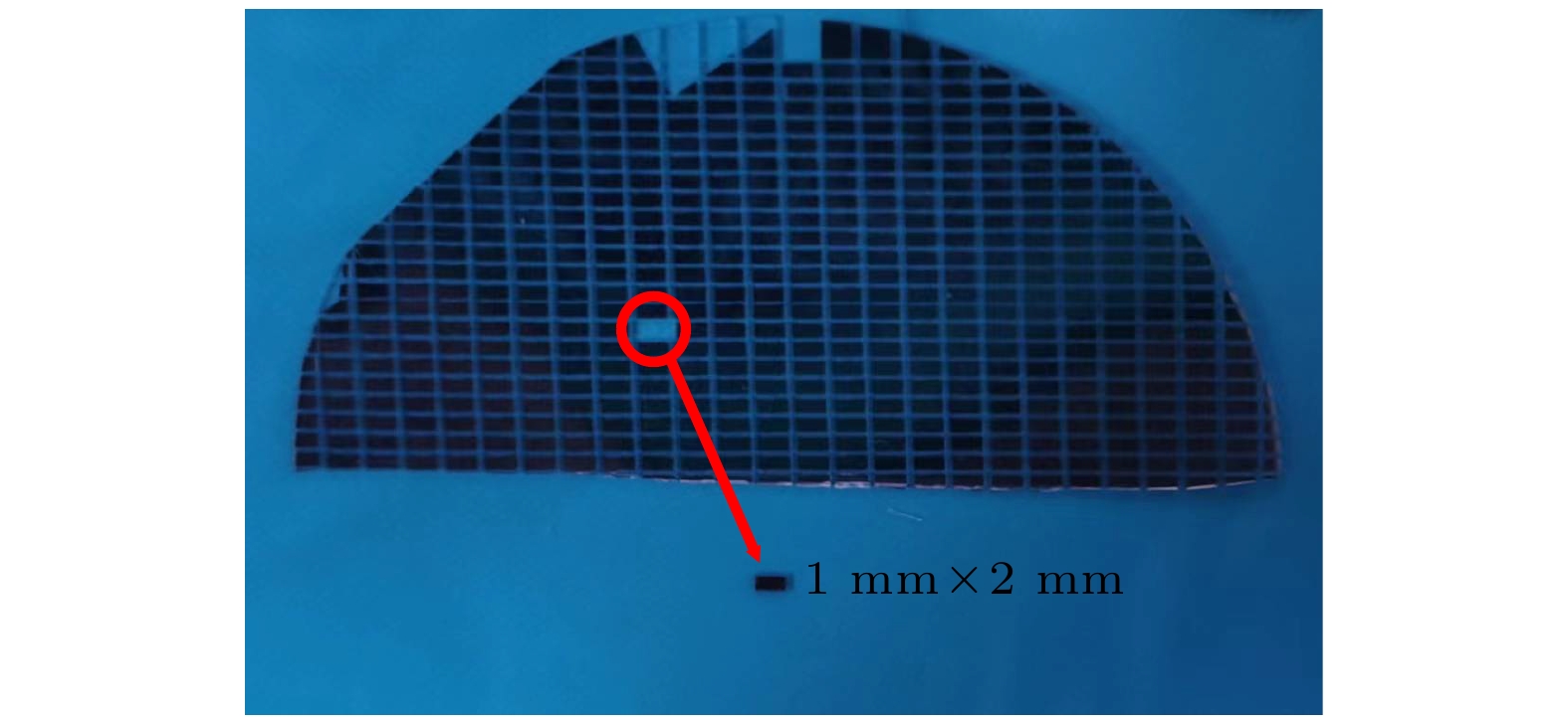
图 13 GeTe薄膜切片照片
Figure 13. Photo of GeTe chips.
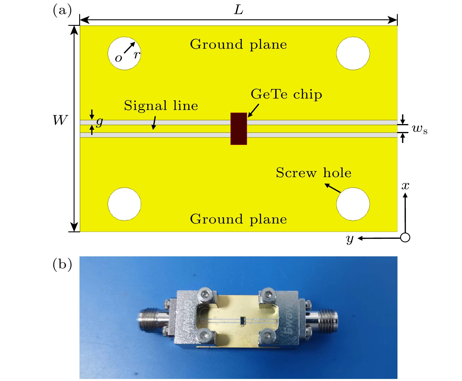
图 14 基于GeTe的并联型开关 (a) 几何结构; (b) 实物样品
Figure 14. Proposed parallel switch using GeTe chip: (a) Geometry; (b) sample.

图 15 基于GeTe的并联型开关等效电路
Figure 15. Equivalent circuit model of the proposed parallel switch using GeTe chip.
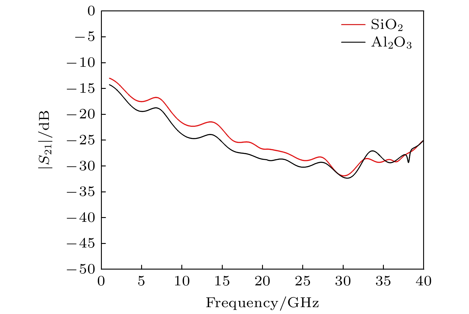
图 16 衬底材料对隔离度的影响
Figure 16. Effect of the substrate material on isolation.
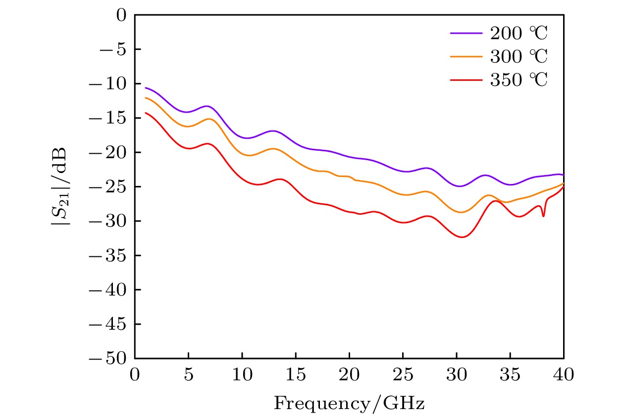
图 19 退火温度对隔离度的影响
Figure 19. Effect of the annealing temperature on isolation.
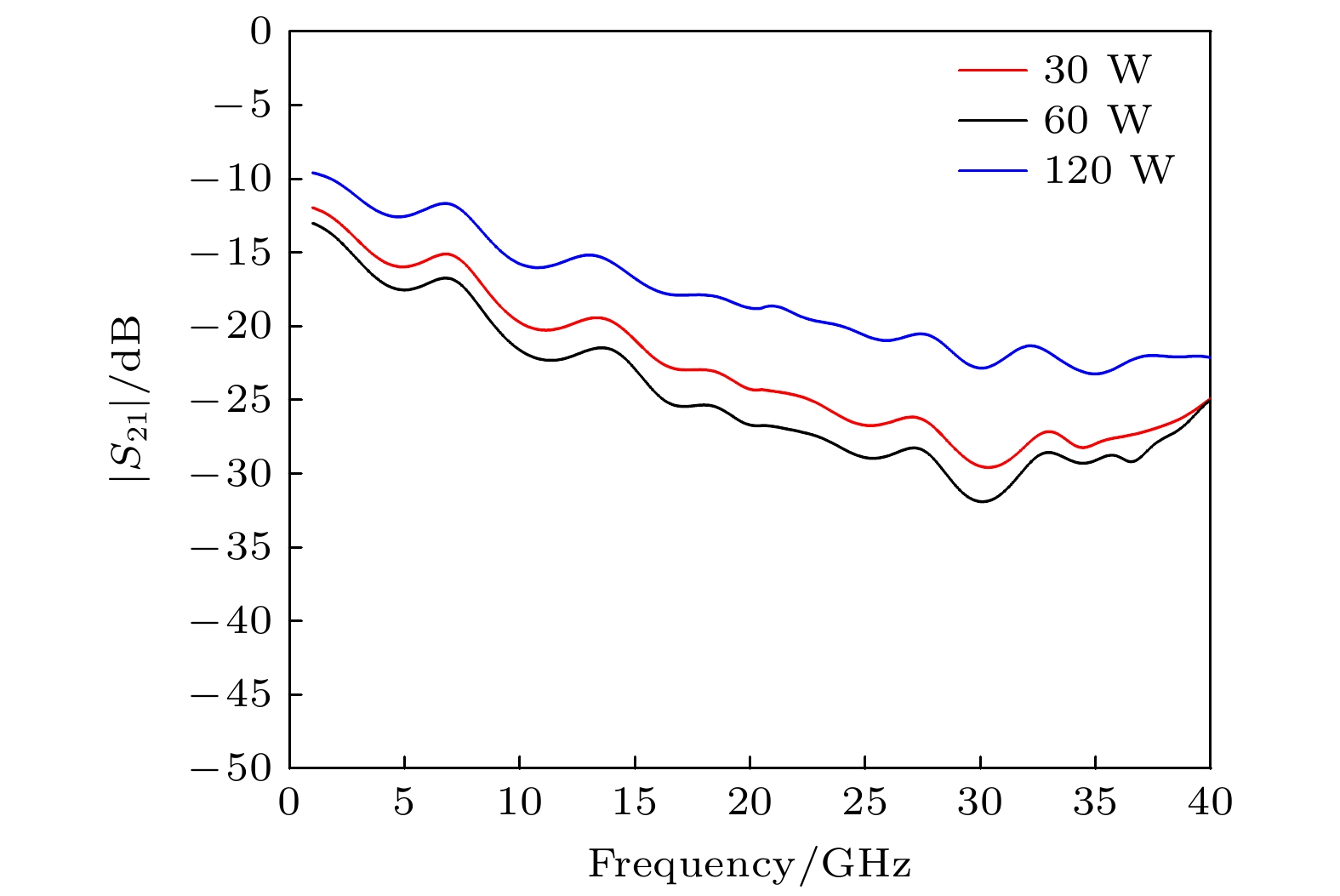
图 17 功率对隔离度的影响
Figure 17. Effect of the deposition power on isolation.
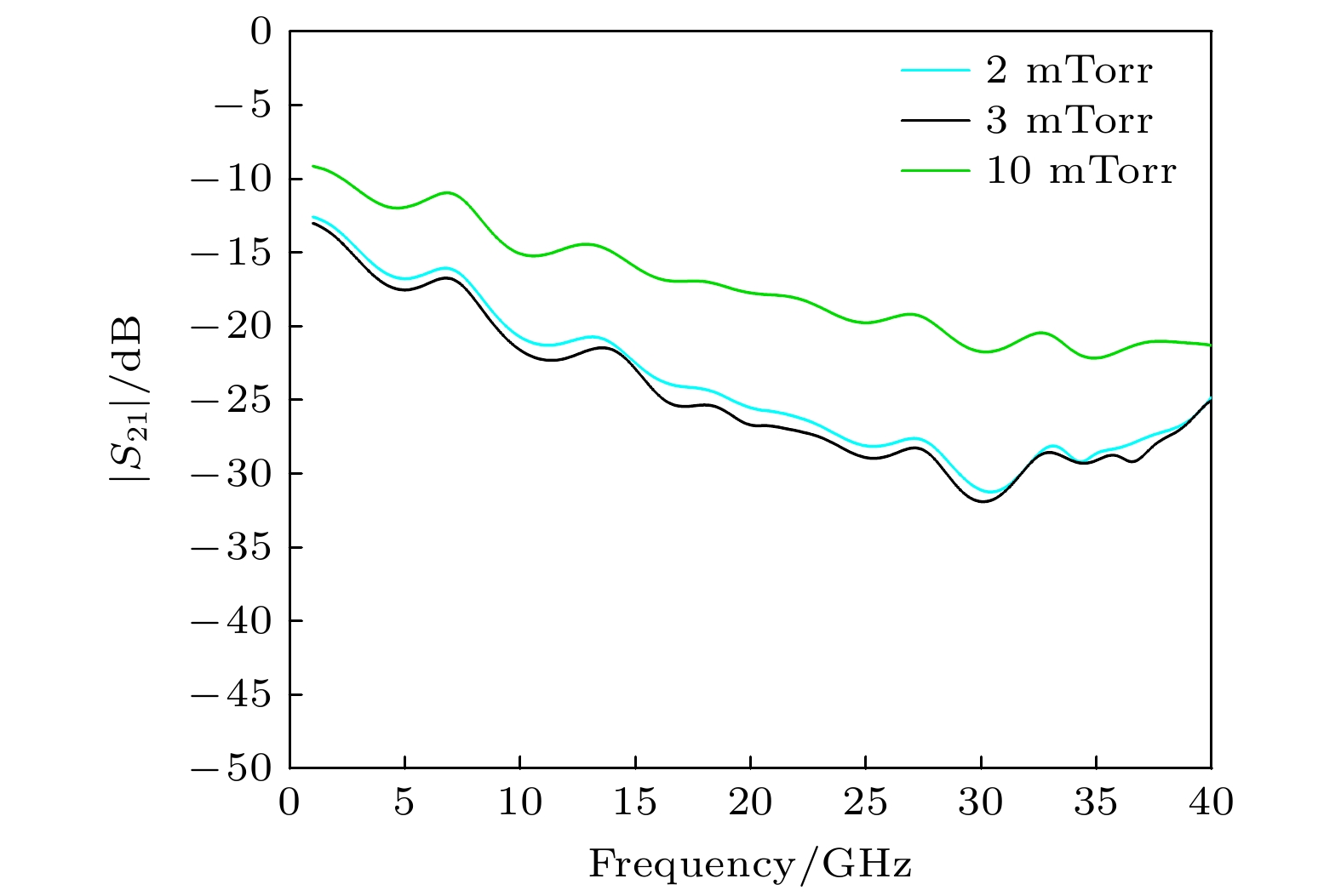
图 18 压强对隔离度的影响
Figure 18. Effect of the deposition pressure on isolation.
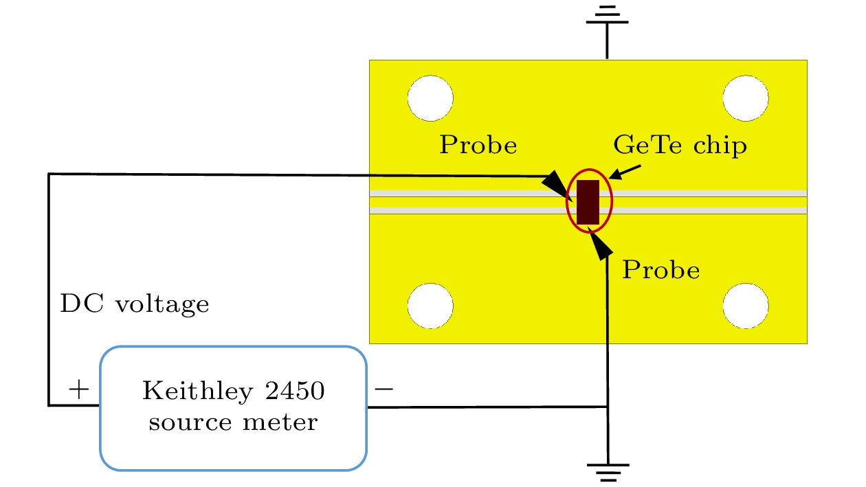
图 20 基于GeTe的并联型开关电阻测试图
Figure 20. Schematic diagram of resistance measurement for GeTe parallel switch.
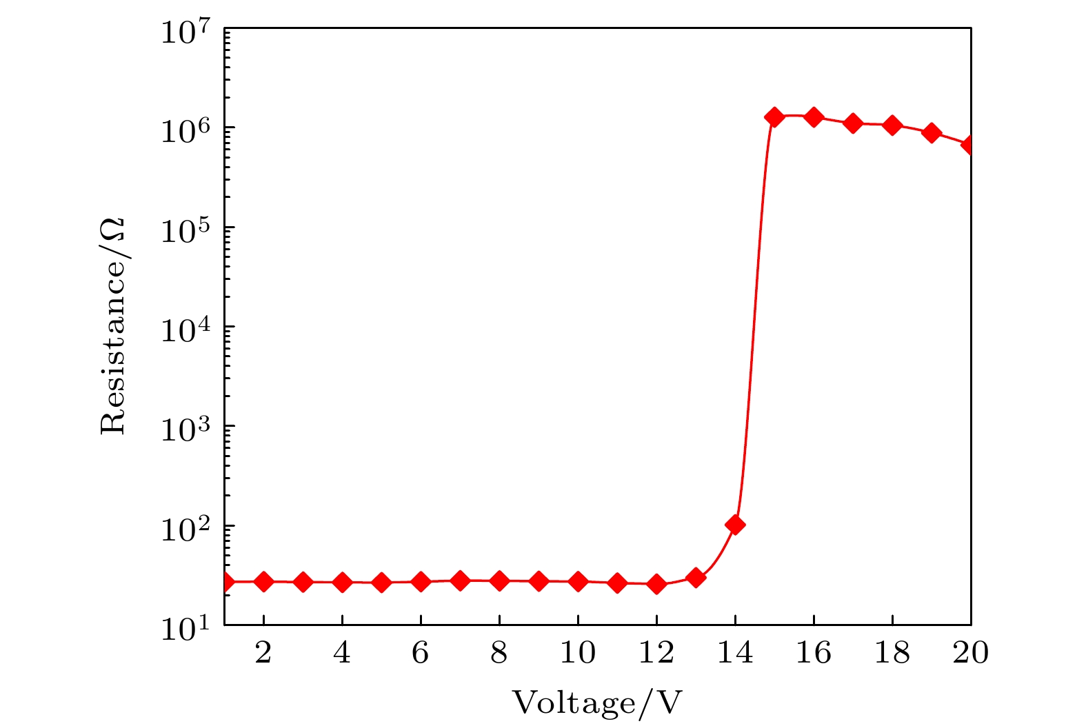
图 21 电阻随脉冲电压的变化
Figure 21. Change curve of the resistance as a function of pulse magnitude.
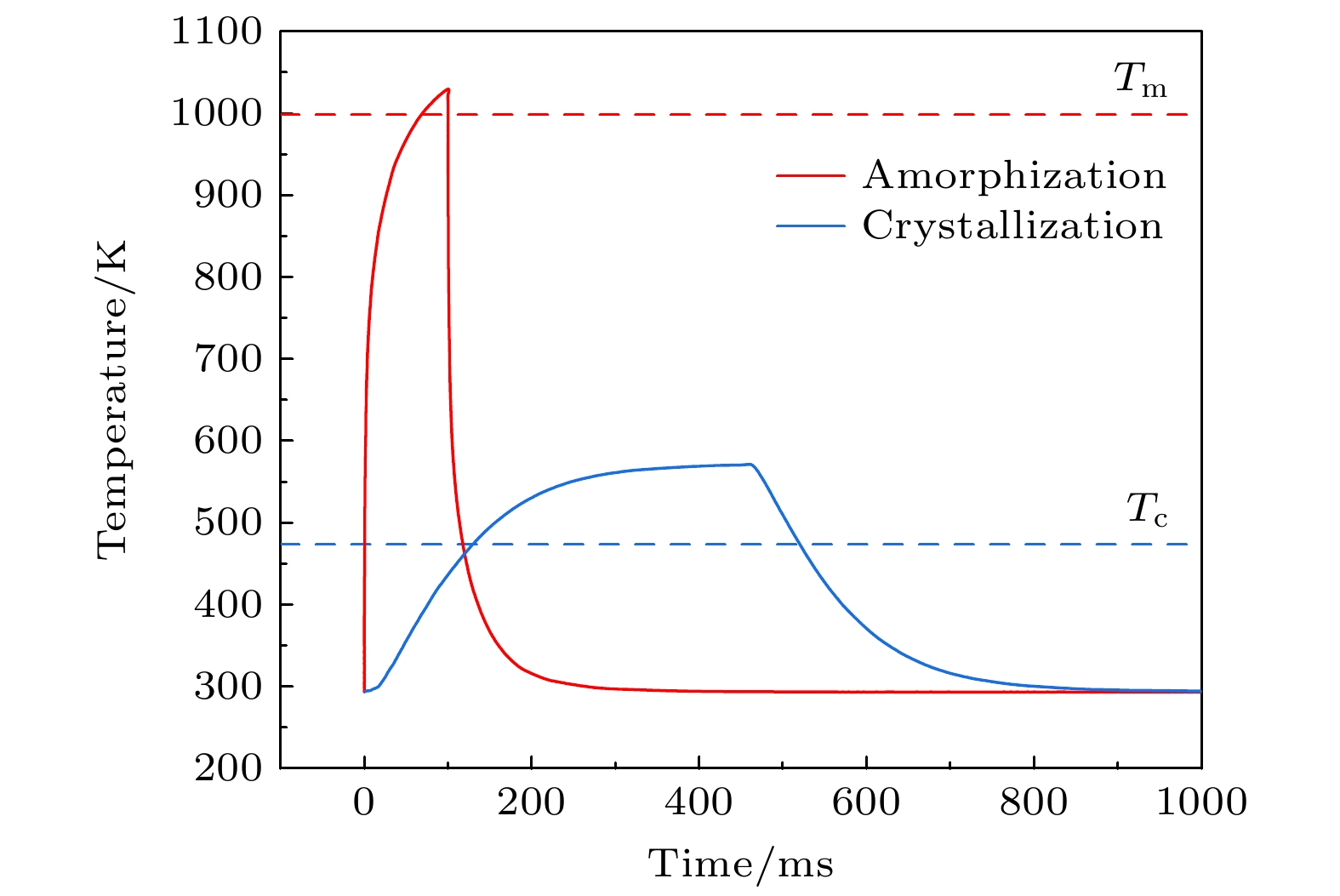
图 22 GeTe薄膜温度随时间的变化
Figure 22. Temperature change on the surface of GeTe film as a function of time.
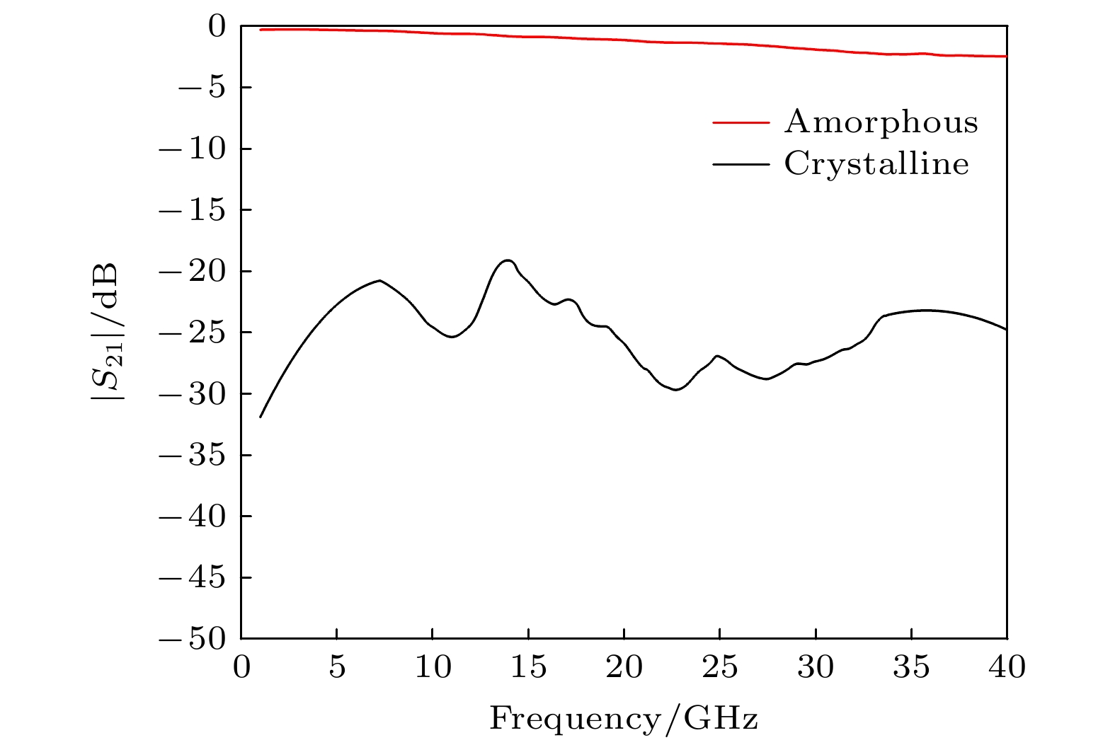
图 23 并联开关测试结果
Figure 23. Measured results for the proposed parallel switch.
表 1 不同衬底的GeTe薄膜方阻
Table 1. Sheet resistance of GeTe Films for different substrates.
序
号衬底
类型溅射条件 退火条件 方阻/
($\Omega\cdot \square^{-1} $)1 SiO2 120 W, 10 mTorr 350 ℃, 30 min 67.8 2 Al2O3 120 W, 10 mTorr 350 ℃, 30 min 66 3 SiO2 80 W, 4 mTorr 350 ℃, 30 min 37.2 4 Al2O3 80 W, 4 mTorr 350 ℃, 30 min 33.8 5 SiO2 60 W, 3 mTorr 350 ℃, 30 min 36 6 Al2O3 60 W, 3 mTorr 350 ℃, 30 min 30  DownLoad: CSV
-
[1] Rangan S, Rappaport T S, Erkip E 2014 Proc. IEEE 102 366
Google Scholar
[2] Wu Z Y, Lu W, Bao X Y, Meng F B, Yang Z B, Sun Q, Zhao F Z, Wang Y T 2021 Int. J. Mod. Phys. B 35 15017
Google Scholar
[3] Sun P, Upadhyaya P, Jeong D, Jeong D H, Heo D, La Rue G S 2007 IEEE Microw. Wirel. Co. 17 352
Google Scholar
[4] Doan C H, Emami S, Niknejad A M, Brodersen R W 2005 IEEE J. Solid-State Circuits 40 144
Google Scholar
[5] Wolf R, Joseph A, Botula A, Slinkman J 2009 IEEE Topical Meeting on Silicon Monolithic Integrated Circuits in RF Systems San Diego, USA, January 19–21, 2009 p1
[6] Campbell C F, Dumka D C 2010 IEEE MTT-S International Microwave Symposium Anaheim, USA, May 23–28, 2010 p145
[7] Daneshmand M, Mansour R R 2011 IEEE Microw. Mag. 12 92
Google Scholar
[8] Boles T, Brogle J, Hoag D, Curcio D 2011 IEEE International Conference on Microwaves, Communications, Antennas and Electronic Systems (COMCAS 2011) Tel Aviv, Israel, November 7–9, 2011 p1
[9] Jaffe M, Abou-Khalil M, Botula A, Ellis-Monaghan J, Gambino J, Gross J, He Z X, Joseph A, Phelps R, Shank S, Slinkman J, Wolf R 2015 IEEE 15th Topical Meeting on Silicon Monolithic Integrated Circuits in RF Systems San Diego, USA, January 26–28, 2015 p30
[10] Stefanini R, Chatras M, Blondy P, Rebeiz G M 2011 IEEE MTT-S International Microwave Symposium Digest, Baltimore MD, USA, June 5–10, 2011 p1
[11] Grant P, Denhoff M, Mansour R R 2004 Proceedings of the IEEE International Conference on MEMS, NANO and Smart Systems (ICMENS) Banff, Canada, August 25–27, 2004 p515
[12] Tabata O, Tsuchiya T 2014 Reliability of MEMS: Testing of Materials and Devices (Hoboken: John Wiley & Sons) pp124–130
[13] Pan K, Wang W, Shin E, Freeman K, Subramanyam G 2015 IEEE T. Electron Dev. 62 2959
Google Scholar
[14] Morin F J 1959 Phys. Rev. Lett. 3 34
Google Scholar
[15] Bahl S K, Chopra K L 1970 J. Appl. Phys. 41 2196
Google Scholar
[16] Raoux S, Cheng H Y, Munoz B, Jordan-Sweet J 2009 European Phase Change and Ovonic Science Symposium, 2009 p91
[17] Raoux S, Ielmini D, Wuttig M, Karpov I 2012 MRS Bull. 37 118
Google Scholar
[18] Raoux S, Cheng H Y, Caldwell M A, Wong H S P 2009 Appl. Phys. Lett. 95 071910
Google Scholar
[19] Fantini P 2020 J. Phys. D Appl. Phys. 53 283002
Google Scholar
[20] Chua K, Shi L P, Zhao R, Lim K G, Chong T C, Schlesinger T E, Bain J A 2010 Appl. Phys. Lett. 97 183506
Google Scholar
[21] Wuttig M 2005 Nat. Mater. 4 265
Google Scholar
[22] Iwasaki H, Ide Y, Harigaya M, Kageyama Y, Fujimura I 1992 J. Appl. Phys. 31 461
Google Scholar
[23] Singh T, Mansour R R 2018 IEEE MTT-S International Microwave Workshop Series on Advanced Materials and Processes for RF and THz Applications (IMWS-AMP) Ann Arbor, USA, July 16–18, 2018 p3
[24] Bettoumi I, Gall N L, Blondy P 2022 IEEE Microw. Wirel. Co 32 52
Google Scholar
[25] Cruz L D L, Ivanov T, Birdwell A G, Weil J D, Kingkeo K, Zaghloul M 2023 IEEE Electron Device Lett. 70 4178
Google Scholar
[26] Charlet I, Guerber S, Naoui A, Charbonnier B, Dupré C, Lugo-Alvarez J, Hellion C, Allain M, Podevin F, Perret E 2024 IEEE Electron Device Lett. 45 500
Google Scholar
[27] Kolobov A V, Fons P, Frenkel A I, Ankudinov A L, Tominaga J, Uruga T 2004 Nat. Mater. 3 703
Google Scholar

 DownLoad:
Catalog
Metrics
- Abstract views: 4602
- PDF Downloads: 104
- Cited By: 0
