


Vol. 69, No. 5 (2020)
2020-03-05
COVER ARTICLE
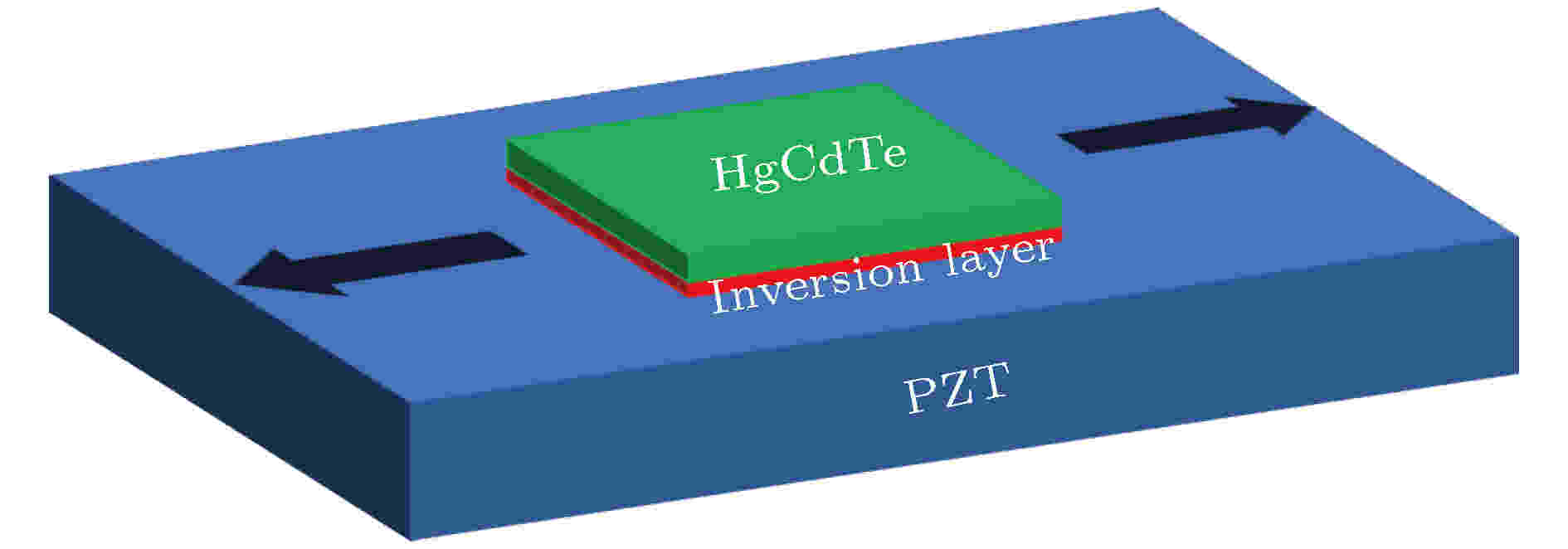
In recent years, the research on topological materials, including topological insulator and topological semimetal, has received a lot of attention in condensed matter physics. HgCdTe, widely used in infrared detection, also holds huge potential in this field. It has been reported that the strained thin Hg0.865Cd0.135Te can realize topological insulator phase by using a CdZnTe substrate. However, the stress caused by changing substrate has great limitations. For example, the stress cannot be changed once the sample has been grown. Hence, we try to use a piezoceramics (PZT) instead to implement the stress and control the properties of HgCdTe. The main purpose of our experiment is to verify its validity. As is well known, the band structure of Hg1–xCdxTe can be precisely controlled by changing the content of Cd. When x lies between 0 and 0.165, HgCdTe features an inverted band structure, which is the premise of realizing topological phase. In this work, an inversion layer is induced on a single crystal grown HgCdTe bulk material by anodic oxidation, whose content of Cd is confirmed to be 0.149 by using XRD. Then the sample is thinned and attached to a PZT, which the tuning of stress is realized by applying a voltage to. Ohmic contacts are realized by indium in van der Pauw configuration. All measurements are carried out by using an Oxford Instruments 4He cryostat with magnetic field applied perpendicularly to the sample plane. At 1.5 K and zero voltage, an evident SdH oscillation is observed. By fitting the linear relationship between filling factor and the reciprocal of magnetic field, the concentration is obtained to be ${n_{\rm{s}}} = 1.25 \times {10^{16}}\;{{\rm{m}}^{ - 2}}$ . Subsequently, we scan the voltage from 200 V to –200 V continuously in different magnetic fields. Two phenomena with different characteristics are observed. It is found that the resistance changes linearly with stress at zero field while an SdH oscillation-like behavior occurs at high field. We attribute such a difference to the existence of two conductive channels: one is the bulk material and the other is the two-dimensional electron gas. It is also noteworthy that the topological phase in our sample cannot be determined because the quantum Hall conductance is polluted by the conductance of bulk material. In conclusion, our results show that it is an effective way to use the PZT to tune the stress and this method can also be applied to the research of other materials.
Zhang Song-Ran,
He Dai-Hua,
Tu Hua-Yao,
Sun yan,
Kang Ting-Ting,
Dai Ning,
Chu Jun-Hao,
Yu Guo-Lin
Acta Physica Sinica.2020, 69(5): 057301.

REVIEW

EDITOR'S SUGGESTION
2020, 69 (5): 054203.
doi: 10.7498/aps.69.20191735
Abstract +
As a novel hybrid quantum system, cavity optomechanical system shows super strong coupling strength, extremely low noise level and considerable coherent time under superconducting condition. In this paper, we briefly introduce basic principles of cavity optomechanics and cavity optomechanical systems. Meanwhile, we also classify the widely studied cavity optomechanical systems as five categories in their materials and structures. Significant parameters of these optomechanical systems, such as quality factor, mass and vibrating frequency of mechanical oscillator, are listed in detail. Technical merits and defects of these optomechanical systems are summarized. Furthermore, we introduce the research progress of non-classical microwave quantum states preparation by utilizing generalized cavity optomechanical systems, and we also analyze the performance advancements and remaining problems of this preparation method. In the end, we summarize the application cases at present and look forward to the potential application scenarios in the future. Our summary may be helpful for researchers who are focusing on quantum applications in sensing, radar, navigation, and communication in microwave domain.

GENERAL

Application of electrical action to design and analysis of magnetically driven solid liner implosion
2020, 69 (5): 050701.
doi: 10.7498/aps.69.20191690
Abstract +
As a typical cylindrical-convergent drive technique, magnetically driven solid liner implosion could compress interior substance with a shock or quasi-isentropic manner, which has been widely used to investigate the hydrodynamic behavior, the dynamic characteristics of material and fusion energy and so on. For aspecific facility, the implosion parameters depend on material, radius and thickness of the liner, and the ablation of liner restrict the optional parameters. The concept of electrical action is introduced via thin shell model, which not only is the representation of states for conductive metal, but also indicates the change of liner velocity under the condition of thin shell hypothesis. The result shows that the outer velocity of liner increases linearly with electrical action and is directly proportional to liner thickness but inversely proportional to liner density. The incompressible zero-dimensional model is used to calculate the dynamic parameters of thin shell liner, including the implosion time, the outer interface velocity, the implosion kinetic energy, and the electrical action under the condition of low linear current density. There exist optimal radius and thickness which can achieve the maximum velocity, momentum, and kinetic energy. The aluminum is suitable for reaching higher velocity and the copper can obtain higher pressure according to a proportionality coefficient Qb/ρ which is an intrinsic quality of metal. A one-dimensional (1D) elastic plastic magnetic hydrodynamic code which is called SOL1D is developed to simulate liner implosion behavior. The modified relationship between resistivity and electrical action is introduced to SOL1D, which can adapt higher hydrodynamic pressure. According to current waves, the 1D code can be used to simulate liner implosion behavior for all kinds of current densities. The 1D simulation liner velocity is in agreement with both the experimental results and the electrical action model for liner implosion experiment on FP-1 facility. The simulation of isentropic compression experiment at ZR facility shows that the magnetic diffusion process is suppressed at extra high current density and hydrodynamic pressure, and the electrical action is larger than the experimental value of wire electrical explosion. The zero-dimensional (0D) and 1D simulation show that estimating the liner velocity and liner phase changing via the electrical action are suitable when thin shell hypothesis and low current density assumption are satisfied.
NUCLEAR PHYSICS

2020, 69 (5): 052901.
doi: 10.7498/aps.69.20191157
Abstract +
One of the grand challenges in ultrafast science is real-time visualization of the microscopic structural evolution on atomic time and length scales. A promising pump-probe technique using a femtosecond laser pulse to initiate the ultrafast dynamics and another ultrashort electron pulse to probe the resulting changes has been developed and widely used to study ultrafast structural dynamics in chemical reactions, phase transitions, charge density waves, and even biological functions. In the past three decades, a number of different ultrafast electron guns have been developed to generate ultashort electron sources, mainly including hybrid electron gun with radio-frequency (RF) cavities for compressing the pulse broadening, relativistic electron gun for suppressing the coulomb interaction, single-electron pulses without space charge effect and compact direct current (DC) electron gun for minimizing the electron propagation distance. At present, these developments with different final electron energy and available total charge have improved the time response of ultrafast electron diffraction (UED) setups to a new frontier approaching to 100 fs regime. Although enormous efforts have been made, the superior capabilities and potentials of ultrafast electron diffraction (UED) are still hindered by space-charge induced pulse broadening. Besides, the penetration depth of electrons increases with the electron energy, while the scattering probability of electrons has the opposite consequence. Thus, in addition to the temporal resolution enhancement, it is also important that the electron energy should be tunable in a wide range to meet the requirements for samples with different thickness. Here in this work, we design a novel ultra-compact electron gun which combines a well-designed cathode profile, thereby providing a uniform field and a movable anode configuration to achieve a temporal resolution on the order of 100 fs over an accelerating voltage range from 10 kV to 125 kV. By optimizing the design of the high-voltage electrode profile, the field enhancement factor on the axis and along the cathode surface are both less than ~4% at different cathode-anode spacings, and thus the maximum on-axis field strength of ~10 MV/m is achieved under various accelerating voltages. This effectively suppresses the space charge broadening effect of the electron pulse. Furthermore, the anode aperture is designed as a stepped hole in which the dense sample grid can be placed, and the sample under study is directly supported by the grid and located at the anode, which reduces the cathode-to-sample distance, thus minimizing the electron pulse broadening from the cathode to sample. Moreover, the defocusing effect caused by the anode hole on the electron beam can be effectively reduced, therefore improving the lateral focusing performance of the electron beam.
ATOMIC AND MOLECULAR PHYSICS

2020, 69 (5): 053101.
doi: 10.7498/aps.69.20191775
Abstract +
Hydrogen-induced cracking (HIC) is a key problem restricting the application of ultra-high strength steel. It is necessary to analyze the distribution of diffusible hydrogen to reveal the mechanism of HIC. The site occupation tendency of H in interstitial and vacancy positions are investigated by the ab-initio method, and the stable configuration and steady state energy are obtained. The solution tendency of H atom in interstitial and vacancy positions is analyzed based on the aforementioned results. Specifically, the Mulliken population, density of states, charge density difference are calculated and used to analyze the interaction between α-Fe metal and H atom. The results show that the dissolved H tends to occupy the interstitial sites of the body-centered cubic, the weak hybridization interaction between the interstitial hydrogen and its nearest neighbour Fe atom is contributed by the H 1s orbital and Fe 4s orbital. Vacancies can capture H atoms easily and H atoms tend to occupy the isoelectric surface near the inwall of the vacancies. A vacancy defect can hold up to three H atoms which are difficult to combine with each other to form H2 molecule by covalent bond. H atoms in vacancies and at interstitial positions change the charge distribution of the Fe lattice, which weakens the binding force of the atoms and forms anti-bonding orbital in local area. The proposed thermodynamical model allows the determining of the equilibrium vacancy and the dissolved H concentration for a given temperature and H chemical potential in the reservoir, and the calculated results are in good agreement with the actual results.

2020, 69 (5): 053201.
doi: 10.7498/aps.69.20191814
Abstract +
With the development of the intense light source, such as free electron lasers, the experiments on the nonlinear process in atomic photo absorption in the XUV and X-ray region became more and more feasible. As one of the simplest possible nonlinear processes, the sequential two-photon double ionization, in which the first photon produces an ion which is subsequently ionized by the second photon, attracts increasing attention of theorists and experimentalists. Study on the angular distributions and angular correlations of the photoelectrons in the sequential two-photon double ionization process are especially attractive, which provides valuable information about the electronic structure of atom or molecule systems and allows the obtaining of additional information about mechanism and pathway of the two-photon double ionization. In this paper, the expression for the photoelectron angular distribution in a sequential two-photon process is given based on the multi-configuration Dirac-Fock method and the density matrix theory. And then, the relativistic calculation program for photoelectron angular distribution is further developed with the help of the program packages GRASP2K and RATIP which are based on the multi-configuration Dirac-Fock method. By using this code, the sequential two-photon double ionization of the 3p shell in atomic argon is studied theoretically. The cross section, magnetic cross section, alignment of residual ions and the asymmetry parameter of the photoelectron angular distribution, each as a function of photon energy, for the first and the second step of sequential two-photon double ionization of argon are presented. The calculations predict that the alignment has a maximum value and the asymmetry parameter has a minimum value in the region of the cooper minimum. The angular distribution of the first step ionization for Ar atom and the second step ionization for Ar+ ion are given at 33.94 eV and 55.34 eV photon energy, respectively. In addition, the difference in property between the angular distributions of the first photoelectron in sequential two-photon double ionization and in conventional one-photon single ionization is discussed. The present calculated results are compared with other available results, showing that they are in good agreement with each other. The results of this paper will be helpful in studying nonlinear processes in the XUV range.
2020, 69 (5): 053301.
doi: 10.7498/aps.69.20191723
Abstract +
ELECTROMAGNETISM, OPTICS, ACOUSTICS, HEAT TRANSFER, CLASSICAL MECHANICS, AND FLUID DYNAMICS
EDITOR'S SUGGESTION
2020, 69 (5): 054201.
doi: 10.7498/aps.69.20191531
Abstract +
In order to improve the resolution of terahertz near-field microscopic imaging technology, an ultra-thin thickness-graded silver-plated strip probe with the same duty cycle is designed to realize the excitation of spoof surface plasmons. By comparing with two other probes with different structures, it can be found that the thickness-graded silver-plated strip probe can produce a strong electric field enhancement effect. Thereafter, the influence of the polarization direction of the incident electric field and the number of periodic metal stripes on the electric field which are generated at the tip of the probe is investigated. It is found that this case is highly consistent with the electric field distribution in Richards-Wolf vector diffraction theory when the incident light is linearly polarized. The electric field intensity generated at the tip of the thickness-graded silver-plated strip probe can be flexibly and effectively manipulated by changing the polarization direction of the incident electric field. When the number of thickness-graded silver-plated strips is 12, the minimum size of the focal spot is 20 μm, which is λ/150. When the number of thickness-graded silver-plated strips is 4, the electric field intensity enhancement factor at the focal spot is 849. The electric field intensity enhancement factor at the focal spot increases continuously as the number of periodic metal stripes increases, and the size of focal spot decreases continuously as the number of periodic metal stripes decreases. This result shows that the tight focusing and electric field enhancement of terahertz waves can be achieved by using an ultra-thin thickness-graded silver-plated strip probe. The research results in this paper have important guiding significance for manipulating the electric field in the terahertz band.
2020, 69 (5): 054202.
doi: 10.7498/aps.69.20191732
Abstract +
In the past decade, most of researchers have been devoted to broadening the bandwidth of absorber. There are few researches on how to achieve wide-angle absorbing materials by detailed theoretical analysis and design guidance. It is still difficult to design wide-angle absorbers. In this paper, based on the equivalent medium theory, the reflectivity of the metamaterial absorber with a single-layered medium backed with metal reflector is analyzed in detail. Starting from the basic electromagnetic theory, the reflection coefficient of the absorber under transverse electric(TE) plane wave and transverse magnetic (TM) plan wave irradiation are derived. And the equivalent electromagnetic parameters of realizing the wide-angle absorbing effect are analyzed, which provide a theoretical basis for designing the wide-angle metamaterial absorber. The theoretical analysis results show that the equivalent electromagnetic parameters required for the medium to achieve low-profile and wide-angle absorbing effect are mainly related to the equivalent permeability and have little relationship with the equivalent permittivity. Moreover, the equivalent electromagnetic parameter value for achieving ultra-wide-angle absorber under TE wave and that under TM wave irradiation are different from each other. In other words, the anisotropic metamaterial with appropriate equivalent permeability has the potential to be used to design the ultra-wide-angle absorbers which are not sensitive to TE waves nor TM waves. In addition, in order to find the theoretically achievable widest absorbing angle value under TE wave and TM wave irradiation, the reflection coefficients at all angles must be less than or equal to –10 dB to obtain the relationship among the equivalent electromagnetic parameters, thickness and angle. The results show that the theoretically achievable widest absorbing angle value is 86.56° under TE wave and TM wave irradiation. The designer can choose the corresponding thickness and permeability from the data obtained from the analysis according to the design requirements. The narrow-band absorbers have limited applications. Therefore, in this paper we also theoretically analyze the values of the equivalent electromagnetic parameters for ahcieving wide-band and wide-angle absorbing materials, and make theoretical verification. The results show that the wide-band and wide-angle absorber can be achieved theoretically, while the equivalent electromagnetic parameters of the medium vary with frequency as some special curves indicate. Although this method is based on the equivalent medium theory and has no direct relationship with the actual structure, it does provide theoretical guidance for designing the wide-angle absorbers.
2020, 69 (5): 054204.
doi: 10.7498/aps.69.20191787
Abstract +
2020, 69 (5): 054205.
doi: 10.7498/aps.69.20191799
Abstract +
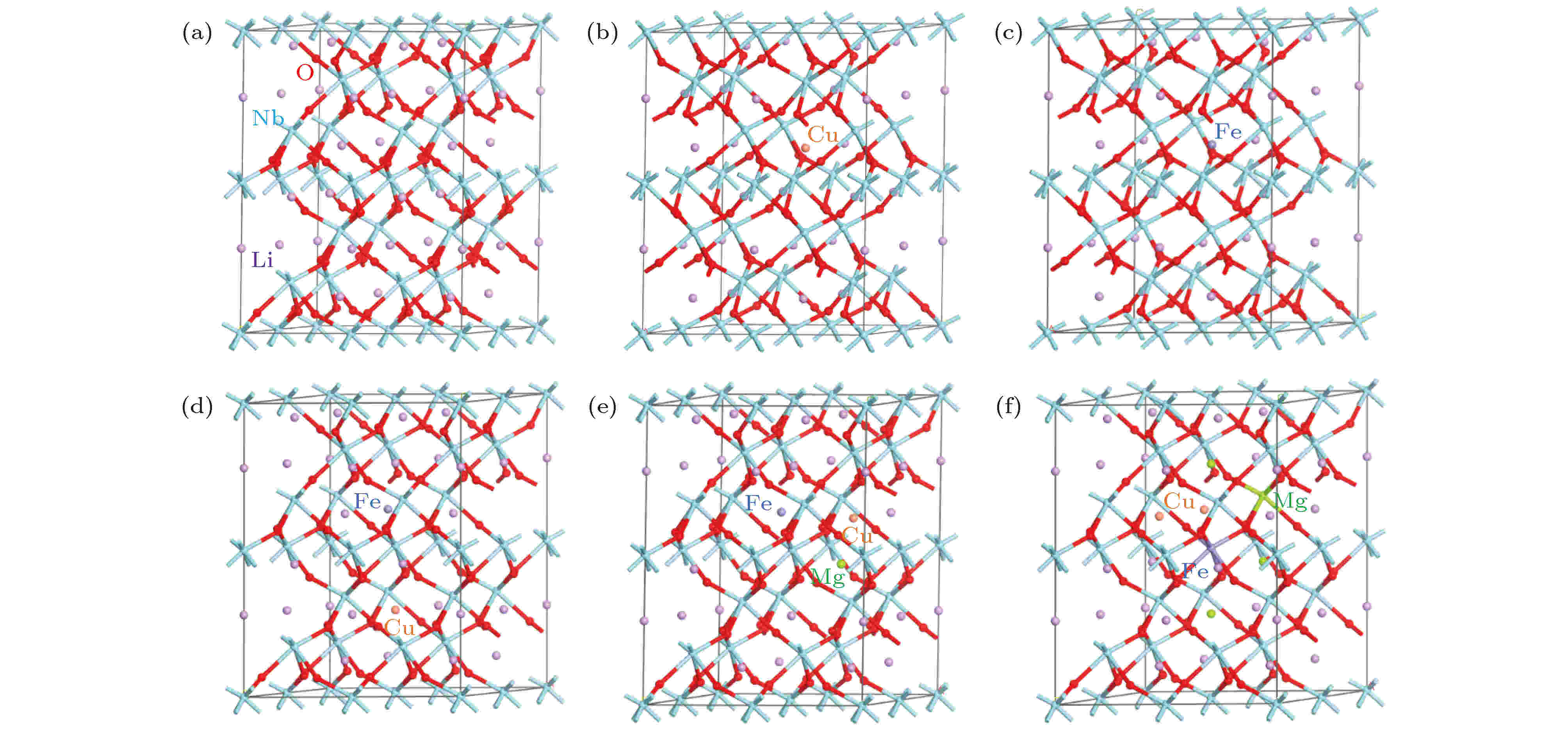
In this paper the electronic structures and optical properties of Cu:Fe:Mg:LiNbO3 crystals and their comparative groups are investigated by first-principles based on the density functional theory to explore the characteristics of charge transfer in crystals and analyse the parameters of the two-colour holographic storage technology based on optical properties of crystals. The basic crystal model is built as a supercell structure 2 × 2 × 1 of near-stoichiometric pure LiNbO3 crystal with 120 atoms, including 24 Li atoms, 24 Nb atoms and 72 O atoms. Above that the five doped crystal models are established as follows: the copper doped LiNbO3 crystal (Cu:LiNbO3), the ferri doped LiNbO3 crystal (Fe:LiNbO3), the copper and ferri co-doped LiNbO3 crystal (Cu:Fe:LiNbO3), the copper, ferri and magnesium tri-doped LiNbO3 crystal (Cu:Fe:Mg:LiNbO3) with doping ions at Li sites, and the copper, ferri and magnesium tri-doped LiNbO3 crystal (Cu:Fe:Mg(E):LiNbO3) with ferri ions at Nb sites and magnesium ions at both Li sites and Nb sites. The last two models represent the concentration of Mg ions below the threshold (~6.0 mol%) and over the threshold respectively. The charge compensation forms are taken successively as $\small {{\rm{Cu}}_{\rm{Li}}^+}\text-{\rm{V}}_{\rm{Li}}^-$ , $\small {{\rm{Fe}}_{\rm{Li}}^{2+}}\text-{2\rm{V}}_{\rm{Li}}^-$ , ${{\rm{Fe}}_{\rm{Li}}^{2+}}\text-{\rm{Cu}}_{\rm{Li}}^+ \text-{3\rm{V}}_{\rm{Li}}^- $ , ${{\rm{Mg}}_{\rm{Li}}^{+} \text-{\rm{Fe}}_{\rm{Li}}^{2+}}\text- $ ${\rm{Cu}}_{\rm{Li}}^+\text -{4\rm{V}}_{\rm{Li}}^-$ and ${{\rm{3Mg}}_{\rm{Li}}^{+}}\text-{\rm{Mg}}_{\rm{Nb}}^{3-}\text-{\rm{Fe}}_{\rm{Nb}}^{2-} \text-{2\rm{Cu}}_{\rm{Li}}^+$ in doped models. The results show that the extrinsic defect levels within the forbidden band of Cu:LiNbO3 crystal and Fe:LiNbO3 crystal are mainly contributed by the 3d orbits of Cu ions and the 3d orbits of Fe ions respectively. The forbidden band widths are 3.45 eV and 3.42 eV respetively in these two samples. In Cu:Fe:LiNbO3 crystal, the impurity levels are contributed by the 3d orbits of Cu and Fe ions; the forbidden band width is 3.24 eV; the absorption peaks are formed at 1.36, 2.53, and 3.01 eV. The Cu:Fe:Mg:LiNbO3 and Cu:Fe:Mg(E):LiNbO3 crystal presentthe forbidden band width of 2.89 eV and 3.30 eV respectively; the absorption peaks are formed at 2.45, 1.89 eV and 2.89, 2.59 eV, 2.24 eV, respectively. In Cu:Fe:Mg:LiNbO3 crystal, the weak absorption peak at 3.01 eV disappears, beacause of the superposition of the red-shifted absorption edge and the next bigger peak. The peak locations move slightly, which can be explained by the crystal field changing under the different doping concentrations and the different occupying positions of doping ions. In Cu:Fe:Mg(E):LiNbO3 crystal, the absorption peak near 2.5 eV is stronger than that of the other tri-doped crystal, which may be caused by the deference in occupancy among Fe ions. The peak at 2.9 eV can be chosen as erasing light, and the peak at 2.5 eV as write and read light in the two-center nonvolatile holography. The tri-doped crystal with Mg2+ concentration over the threshold shows obvious absorption peak at 2.9 eV and stronger absorption at 2.5 eV, which is beneficial for this application. The strong absorption of write light can shorten the time to reach the saturation of diffraction efficiency, then increase the dynamic range (M/#) and the sensitivity (S). Meanwhile, in this Mg doping condition, write time can be shortened, so optical damage can be weakened, and finally the image quality can be optimized.


2020, 69 (5): 054206.
doi: 10.7498/aps.69.20191449
Abstract +
An ultra-compact 1 × 2 demultiplexer based on multimode interference (MMI) waveguide is proposed to separate the 1310 nm and 1550 nm wavelengths, in which Si3N4/SiNx/Si3N4 sandwiched structure is used to realize polarization insensitivity. Firstly, how to use Si3N4/SiNx/Si3N4 sandwich structure to achieve polarization-independent is discussed. Keeping the width of MMI waveguide WMMI unchanged, the beat lengths of two orthogonal polarization states at same wavelength versus refractive indexes of SiNx are calculated. Similar simulation curves with different WMMI values and wavelengths are also provided. The result shows that there are crossing points in the beat length curves. It means that the beat lengths for the two orthogonal polarization states at the same wavelength can be identical by choosing the proper refractive index of the SiNx. More importantly, under exactly the same premise, for the two wavelengths, their crossing points are almost identical. Then, how to realize the function of wavelength separation is studied. A variable called the beat length ratio is given, which is defined as the beat length ratio of two working wavelengths under the same polarization state. When the beat length ratio equals an even number divided by an odd number, one wavelength is even multiple of beat length and the other wavelength is odd multiple of beat length, and vice versa, that is to say, a single image and a mirror image for the two working wavelengths are formed respectively. Therefore, the two working wavelengths will output from different output ports, therefore the two wavelengths are successfully separated from each other. The demultiplexer based on Si3N4/SiO2 platform has a compact structure, easy integration and good tolerance. Three-dimensional finite-difference time-domain method is used for simulation, and the results show that the size of the MMI waveguide is 4.6 μm × 227.7 μm; the insertion loss and crosstalk are as low as 0.18 dB and –25.7 dB respectively; a broad 3-dB bandwidth of 60 nm is achieved. Moreover, the fabrication deviation of the key structural parameters about the device is discussed in detail, and the insertion loss and crosstalk are considered. To demonstrate the transmission characteristics of the demultiplexer, the evolution of the excited fundamental mode in the demultiplexer is also given. The novel demultiplexer is polarization independent and can work at wavelengths of 1310 nm and 1550 nm simultaneously. It has potential application value in future integrated optical circuits.

2020, 69 (5): 054207.
doi: 10.7498/aps.69.20190997
Abstract +
The common feature of traditional methods of preparing orbital angular momentum (OAM) light beams propagating along the z axis is that the wave-front phase is changed and the chief ray of beam is basically unchanged. But it is difficult to obtain a high $m\hbar $ OAM. To solve the above problem, we establish a theoretical framework based on the change of the chief ray of beam instead of the change of wave-front phase. The differential geometry theory is used to verify the theoretical assumption that the light transmitted by the cylindrical spiral wave-guide can carry high $m\hbar $ OAM. To measure the OAM optical fiber output, we use the diffraction method to detect the phase of vortex, that is, we can use a microscope to observe the phase distribution of optical fiber end face. We consider the output of linearly polarized light along the tangent direction of the fiber to observe its diffraction pattern. The transmission of optical fiber around the cylinder is the main light. The diameter of optical fiber is constant, and the light wave transmitting into the optical fiber is Bessel beam. For the linear fiber output, we need to consider only the linear fiber Bessel beam. The output cross section of the wave surface in the fiber is approximately that of plane wave. When $\theta > {\theta _0}$ , we use the flow coordinates $(\alpha,\beta, \gamma)$ to calculate the diffraction pattern of the cross section of the optical fiber when light travels in the optical fiber around the cylinder, which shows the characteristics of vortex. The optical field distribution carries a high-order OAM mode. When $\theta = {\theta _0}$ , cylindrical orbital optical fibers transit to linear orbital optical fibers. We calculate the diffraction pattern of the cross section of the optical fibers propagating in a straight line. It is an Airy spot, namely a circular aperture diffraction spot. The optical field distribution has no higher-order OAM mode. When the order of the output beam is small, the output shows certain uniformity and symmetry, when the order of the output beam increases gradually, the output beam shows some inhomogeneity and asymmetry.


2020, 69 (5): 054701.
doi: 10.7498/aps.69.20191742
Abstract +
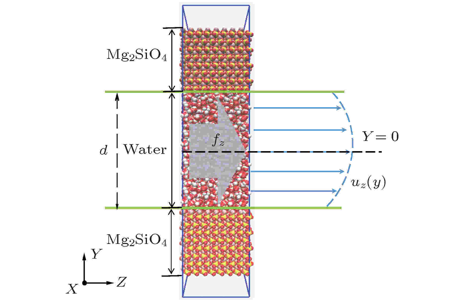
The surface dissolution of rock nanopores, caused by the acidic environment, increases the salt concentration of water solution flowing in the nanopores, thereby destroying the surface structure of the rock, which can be found in CO2 geological sequestration and crude oil and shale gas exploration. In this paper, the molecular dynamics method is adopted to study the flow characteristics of water solution in the forsterite (Mg2SiO4) slit nanopores, by which the effects of salt concentration and structure destruction of pore surface on the velocity profiles of water solution confined in nanopores are systematically analyzed. The hydrogen bond density, radial distribution function (RDF) and water density distribution are calculated to explain the changes in viscosity, velocity profiles and interaction between water and nanopore surface. The results show that as the salt concentration increases, the water solution flow in the rock nanopore obeys the Hagen-Poiseuille equation, and the velocity profiles of water solution remain parabolic shape. However, the hydrogen bond network among water molecules becomes denser with salt concentration increasing, which can account for the linear increase in the viscosity of water solution. Besides, the higher salt concentration gives rise to the larger water flow resistance from the pore surface. As a result, with the salt concentration increasing, the maximum of water velocity decreases and the curvature radius of the parabolic velocity profile curve becomes bigger. Moreover, the surface structure destruction in rock nanopores changes the roughness of surface in the flow channel, which enhances the attraction of nanopore surface to H2O. As the structure destruction of nanopore surface deteriorates, the water density near the rough surface moves upward, whereas the velocity of water near the rough surface declines obviously. Interestingly, when the degree of surface structure destruction reaches 50%, a significant negative boundary slipping near the rough surface appears.
PHYSICS OF GASES, PLASMAS, AND ELECTRIC DISCHARGES
2020, 69 (5): 055201.
doi: 10.7498/aps.69.20191716
Abstract +
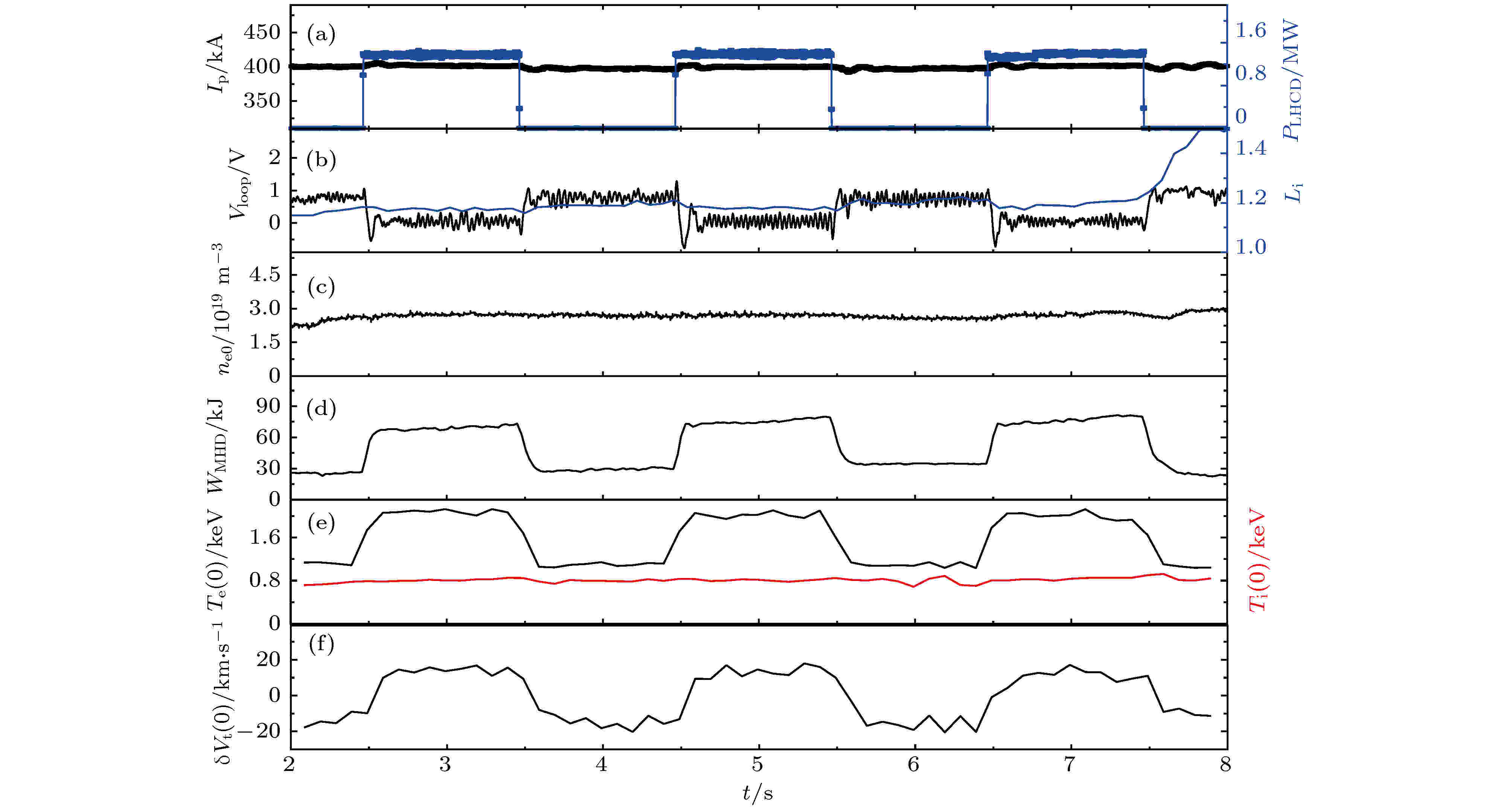
Rotation and its shear can reduce the magnetohydrodynamic instabilities and enhance the confinement. The LHCD has been proposed as a possible means of rotation driving on a future fusion reactor. Exploring the mechanisms of LHCD rotation driving on the current tokamaks can provide important reference for future reactors. On EAST, it was previously shown that 2.45 GHz LHCD can drive plasma toroidal rotation and the change of edge plasma rotation leads the co-current core rotation to increase. At higher frequency, 4.6 GHz lower hybrid wave can more effectively drive co-current plasma toroidal rotation. On EAST, at the lower current, the effects of different LHCD power on plasma toroidal rotation are analyzed. Higher power LHCD has a better driving efficiency. The effect of safety factor (q) profile on toroidal rotation is also presented. The LHCD can change the profile of safety factor due to current drive. It is found that when the power exceeds 1.4MW, the q profile remains unchanged and the rotation changes only very slightly with LHCD power, suggesting that the current profile is closely related to rotation. In order to further analyze the dynamic process of plasma toroidal rotation driven by lower hybrid current drive on EAST, the toroidal momentum transport due to LHCD is deduced by using the modulated LHCD power injection. Based on the momentum balance equation, the toroidal momentum diffusion coefficient (χφ) and the toroidal momentum pinch coefficient (Vpinch) are obtained by the method of separation of variables and Fourier analysis for the region where the external momentum source can be ignored. It is found that the momentum diffusion coefficient (χφ) and momentum pinch coefficient (Vpinch) tend to increase from the core to the outer region. This is consistent with the characteristic that the toroidal rotation velocity first changes in the outer region and then propagates to the core when the toroidal rotation is driven by LHCD.
CONDENSED MATTER: STRUCTURAL, MECHANICAL, AND THERMAL PROPERTIES

EDITOR'S SUGGESTION
2020, 69 (5): 056101.
doi: 10.7498/aps.69.20191209
Abstract +

EDITOR'S SUGGESTION
2020, 69 (5): 056201.
doi: 10.7498/aps.69.20191730
Abstract +
Interfacial mechanical properties have a great influence on the overall mechanical performance of graphene/flexible substrate composite structure. Therefore, it is necessary to study interfacial shear stress transfer between graphene and flexible substrate. In this paper, a two-dimensional nonlinear shear-lag model (2D model) is presented. Taking the effects of Poisson’s ratio of the graphene and substrate into consideration, the bidirectional interfacial shear stress transfer between graphene and flexible substrate subjected to uniaxial tension is investigated by the 2D model when the Poisson’s ratio of substrate is larger than that of graphene. In the elastic bonding stage, the semi-analytical solutions of the bidirectional normal strains of the graphene and bidirectional interfacial shear stresses are derived, respectively, and their distributions at different positions are illustrated. The critical strain for interfacial sliding is derived by the 2D model, and the results show that the critical strain has a micron-scaled characteristic width. The width size of graphene has a significant influence on the critical strain when it is less than the characteristic width, but the size effect can be ignored when the width of graphene is larger than the characteristic width. In addition, the Poisson’s ratio of substrate can also affect the critical strain. Based on the 2D model, the finite element simulations are made to investigate the distribution of graphene's normal strains and interfacial shear stresses in the interfacial sliding stage. Furthermore, compared with the results obtained via one-dimensional nonlinear shear-lag model (1D model), the distributions of graphene’s normal strains and interfacial shear stresses calculated by 2D model show obvious bidimensional effects both in the elastic bonding stage and in the interfacial sliding stage when the width of graphene is large. There exists a compression strain in the graphene and a transverse (perpendicular to the tensile direction) shear stress in the interface, which are neglected in the 1D model. And the distributions of graphene’s tensile strain and longitudinal (along the tensile direction) interfacial shear stress are not uniform along the width, which are also significantly different from the results of 1D model. Moreover, the critical strain for interfacial sliding derived by the 2D model is lower than that obtained by the 1D model. However, when the width of graphene is small enough, the 2D model can be approximately replaced by the 1D model. Finally, by fitting the Raman experimental results, the reliability of the 2D model is verified, and the interfacial stiffness (100 TPa/m) and shear strength (0.295 MPa) between graphene and polyethylene terephthalate (PET) substrate are calculated.

2020, 69 (5): 056301.
doi: 10.7498/aps.69.20191391
Abstract +
Using the first principle calculation based on the density functional theory, we have systematically investigated the structure stability, electronic structure and photocatalytic properties of two-dimensional single-layered GeTe crystal structure modified by H and F. The results show that the lattice constant, bond angle and bond length of GeTe increase after being modified. The stability analysis shows that all the materials have excellent dynamical, mechanical, and thermal stabilities. The electronic structure analysis shows that the two-dimensional GeTe is an indirect bandgap semiconductor with an energy gap of 1.797 eV, and its energy band is mainly composed of Ge-4p and Te-5p, while it is converted into a direct bandgap semiconductor by H or F modification and H-F co-modification (F and Ge on one side, H and Te on the other), and their corresponding energy gaps are reduced to 1.847 eV (fH-GeTe), 0.113 eV (fF-GeTe) and 1.613 eV (hF-GeTe-hH). However, hH-GeTe-hF is still an indirect band gap semiconductor, and its energy gap is reduced to 0.706 eV. The results of the density of states show that part of the Ge-4p and Te-5p electrons are transferred to a deeper level due to the adsorption of H or F atoms, resulting in a strong orbital hybridization between them and the adsorbed atoms. The effective mass shows that the effective mass of H or F modified and H-F co-modified GeTe (F and Ge on one side, H and Te on the other) decrease, and their carrier mobilities increase. The carrier recombination rates of all modified GeTe materials are lower than that of the intrinsic GeTe, so the semiconductor will be more durable. The electron density difference shows that due to the electronegativities of atoms being different from each other, when H or F is used to modify GeTe, some electrons transfer to H and F atoms, resulting in the weakening of covalent bond between Ge and Te atoms and the enhancement of ion bond. The results of band-edge potential analysis show that GeTe can produce hydrogen and oxygen by photolysis of water. However, the valence band edge potential of the modified GeTe decreases significantly, and its oxidation ability increases considerably, the photocatalytic water can produce O2, H2, O3, OH·, etc. Optical properties show that the modified GeTe can enhance the absorption of visible and ultraviolet spectrum, which indicates that they have great application prospects in the field of photocatalysis.

2020, 69 (5): 056501.
doi: 10.7498/aps.69.20191409
Abstract +
Thermal rectification refers to the phenomenon that heat fluxes or equivalent thermal conductivities are different under the same temperature difference when temperature gradient directions are different. The nature of the thermal rectification is that the structure has different effective thermal conductivities in different directions. Most of previous studies focused on thermal rectification of temperature-dependent thermal conductivity materials or variable cross section area structure, and the effect of thermal contact resistance at the interface was investigated very rarely. In the present paper we present the analytical and finite element numerical solution of temperature field and thermal rectification ratios of a composite structure with variable cross section area and thermal conductivity under different interface thermal contact resistances. The prescribed temperature boundary condition is introduced by penalty method, and the temperature jump condition at the interface is implemented by the definition of thermal contact resistance directly. The nonlinear heat conduction problem caused by temperature-dependent thermal conductivity and interface thermal contact resistance is then solved with a direct iteration scheme. Comparisons between experimental results and the present theoretical and numerical results show the feasibility of the proposed model. Then parameter investigations are also conducted to reveal the effect of some key geometric and material parameters. Numerical results show that thermal contact resistance plays an important role in the temperature field and thermal rectification ratio of the two-segment thermal rectifier. With the increase of the length ratio, thermal ratification ratio increases first and decreases then, and the optimal length ratio varies with both thermal contact resistance and cross-section radius change rate of the two segments. In general, the existence of thermal contact resistance can increase the total thermal resistance of the rectifier and magnify the distinction of the heat flux in forward and reverse cases. However, if the thermal contact resistance is too large, this distinction will decrease and correspondingly the thermal rectification ratio becomes low. With the increase of the boundary temperature difference, thermal rectification ratio increases due to the effect of temperature-dependent thermal conductivity. In the present study, we propose a theoretical and numerical approach to designing and optimizing the length ratio, cross-section radius change rate, thermal conductivity, boundary temperature difference and interface thermal contact resistance to obtain the maximal thermal rectification ratio of a bi-segment thermal rectifier, as well as the manipulation of thermal flux in engineering applications.
CONDENSED MATTER: ELECTRONIC STRUCTURE, ELECTRICAL, MAGNETIC, AND OPTICAL PROPERTIES

2020, 69 (5): 057101.
doi: 10.7498/aps.69.20191512
Abstract +

2020, 69 (5): 057201.
doi: 10.7498/aps.69.20191561
Abstract +
Nanocrystalline bulk materials n-type (Bi1–xTbx)2(Te0.9Se0.1)3 (x = 0, 0.002, 0.004, 0.008) are fabricated by high pressure sintering (HPS) technique. The HPS samples are then annealed for 36 h in a vacuum at 633 K. The phase compositions and crystal structure of HPS sample are analyzed by X-ray diffraction. The microscopic morphology of HPS sample is observed by field-emission scanning electron microscopy. The electric conductivity, Seebeck coefficient, and thermal conductivity of the HPS sample and annealed sample are measured in a temperature range from room temperature to 473 K. The effects of Tb content on crystal structure and thermoelectric properties of the sample are systematically studied. The results show that HPS sample consists of nanoparticles. With the increase of content of Tb, the cell volume increases. Besides, the power factor increases but thermal conductivity decreases through doping Tb, thus the optimal figure of merit (ZT) value increases. The Tb doping amount of x = 0.004 is an optimal doping amount. At this doping amount, the maximum ZT of 0.29 is achieved, which is enhanced by 32% compared with the ZT value of undoped sample. The thermoelectric performance can be improved significantly by annealing. The thermal conductivity of the annealed sample with x = 0.004 is 0.9 W·m–1·K–1 at 373 K, decreased by 23% compared with the thermal conductivity of HPS sample. Consequently, the ZT value of annealed sample is significantly higher than that of HPS sample. The maximum thermoelectric ZT of 0.99 is achieved for annealed sample with x =0.004 at 373 K. Furthermore, it is worthwhile to note that this annealed sample possesses a ZT value larger than 0.8 when the temperature is higher than 323 K.
2020, 69 (5): 057202.
doi: 10.7498/aps.69.20191835
Abstract +
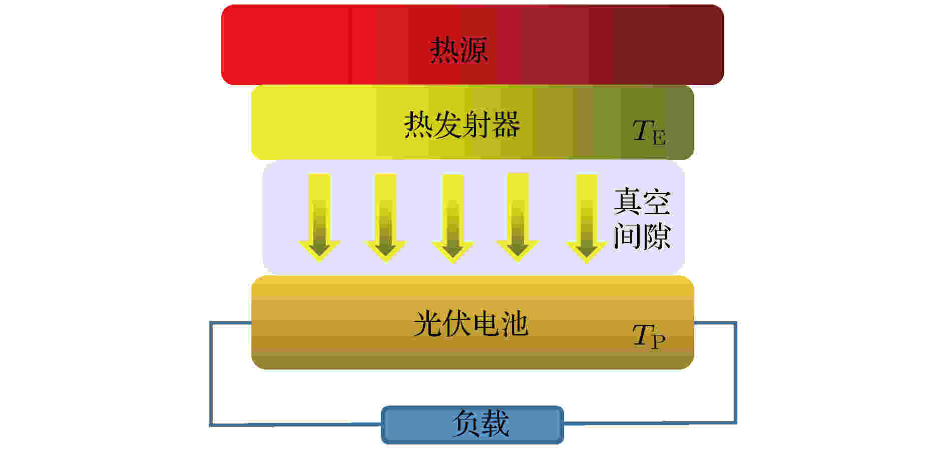
The application of thermophotovoltaic energy conversion device to recovery and utilization of high-grade thermal energy are limited by its irreversible loss. In this work, we reveal the source of irreversible loss and provide a strategy for improving the performance of thermophotovoltaic energy conversion device. The maximum efficiency of thermophotovoltaic energy conversion device under ideal condition is determined by using the theory of semiconductor physics and Planck thermal radiation. Moreover, the effects of non-radiative recombination and irreversible heat transfer loss on the electrical, optical, and thermal characteristics of thermophotovoltaic device are considered to predict the optimal performance of thermophotovoltaic device. The optimal region of power density, efficiency, and photon cut-off energy are determined. The obtained results show that the open-circuit voltage, short-circuit current density and efficiency of non-ideal device are lower than those of ideal device. The voltage output and photon cut-off energy of thermophotovoltaic device and heat source temperature can be optimized to improve the power density and efficiency of the device. It is found that the theoretical results are in good agreement with the experimental results, which can provide some guidances fordeveloping the practical thermophotovoltaic devices.
COVER ARTICLE
2020, 69 (5): 057301.
doi: 10.7498/aps.69.20191330
Abstract +
In recent years, the research on topological materials, including topological insulator and topological semimetal, has received a lot of attention in condensed matter physics. HgCdTe, widely used in infrared detection, also holds huge potential in this field. It has been reported that the strained thin Hg0.865Cd0.135Te can realize topological insulator phase by using a CdZnTe substrate. However, the stress caused by changing substrate has great limitations. For example, the stress cannot be changed once the sample has been grown. Hence, we try to use a piezoceramics (PZT) instead to implement the stress and control the properties of HgCdTe. The main purpose of our experiment is to verify its validity. As is well known, the band structure of Hg1–xCdxTe can be precisely controlled by changing the content of Cd. When x lies between 0 and 0.165, HgCdTe features an inverted band structure, which is the premise of realizing topological phase. In this work, an inversion layer is induced on a single crystal grown HgCdTe bulk material by anodic oxidation, whose content of Cd is confirmed to be 0.149 by using XRD. Then the sample is thinned and attached to a PZT, which the tuning of stress is realized by applying a voltage to. Ohmic contacts are realized by indium in van der Pauw configuration. All measurements are carried out by using an Oxford Instruments 4He cryostat with magnetic field applied perpendicularly to the sample plane. At 1.5 K and zero voltage, an evident SdH oscillation is observed. By fitting the linear relationship between filling factor and the reciprocal of magnetic field, the concentration is obtained to be ${n_{\rm{s}}} = 1.25 \times {10^{16}}\;{{\rm{m}}^{ - 2}}$ . Subsequently, we scan the voltage from 200 V to –200 V continuously in different magnetic fields. Two phenomena with different characteristics are observed. It is found that the resistance changes linearly with stress at zero field while an SdH oscillation-like behavior occurs at high field. We attribute such a difference to the existence of two conductive channels: one is the bulk material and the other is the two-dimensional electron gas. It is also noteworthy that the topological phase in our sample cannot be determined because the quantum Hall conductance is polluted by the conductance of bulk material. In conclusion, our results show that it is an effective way to use the PZT to tune the stress and this method can also be applied to the research of other materials.

2020, 69 (5): 057401.
doi: 10.7498/aps.69.20191540
Abstract +
The ambient gas pressure has an important influence on the laser induced plasma characteristics. The effects of gas pressure on the characteristics of air plasma induced by nanosecond laser are studied by using the optical emission spectroscopy, and the relationship between the gas pressure and the spectral intensity, and between electron temperature and electron density of air plasma are discussed. The air gas pressure in chamber is continuously changed in a range from 10 to 100 kPa by using a mechanical pump and measured by using a barometer. The ns laser energy in experiment is fixed at 100 mJ in the whole experiment. The digital delay trigger (Stanford DG535/645) is used to trigger the laser and ICCD synchronously, and the delay and gate time of ICCD are set to be 0 and 5 μs, respectively. The experimental results show that air plasma emission spectrum consists of the line and continuous spectrum, and the spectral intensity of air plasma emission spectrum is dependent on gas pressure in a range from 10 to 100 kPa, and the evolution of atomic spectrum intensity with gas pressure is different from that of ion spectrum intensity. The air density in the region of laser breakdown increases with air pressure increasing, which leads the breakdown probability of air gas to increase, thus resulting in the air plasma spectral intensity increasing. Under the confinement action of the ambient air gas in the expanding region of air plasma, the collision probability and energy exchange probability among particles in the air plasma are both increased, and the trisomic recombination probability of ion-electron-atom is also increased. As a result, the atomic spectral intensity of O Ι 777.2 nm and N Ι 821.6 nm both increase with the air gas pressure increasing, and the spectral intensity is highest at 80 kPa, and then slowly decreases. But the spectral intensity of N II 500.5 nm reaches its maximum value at 40 kPa, and decreases as the pressure becomes greater than 40 kPa. The electron density of the air plasma increases with the air pressure increasing, and the growth rate becomes slow after 80 kPa. The electron temperature of the air plasma reaches a maximum value at 30 kPa. The plasma electron temperature gradually decreases as the pressure becomes greater than 30 kPa. The research results can provide an important experimental basis for studying the laser-induced air plasma characteristics at different altitudes, and also give important technical support for laser atmospheric transmission and atmospheric composition analysis in the future.
2020, 69 (5): 057501.
doi: 10.7498/aps.69.20191622
Abstract +
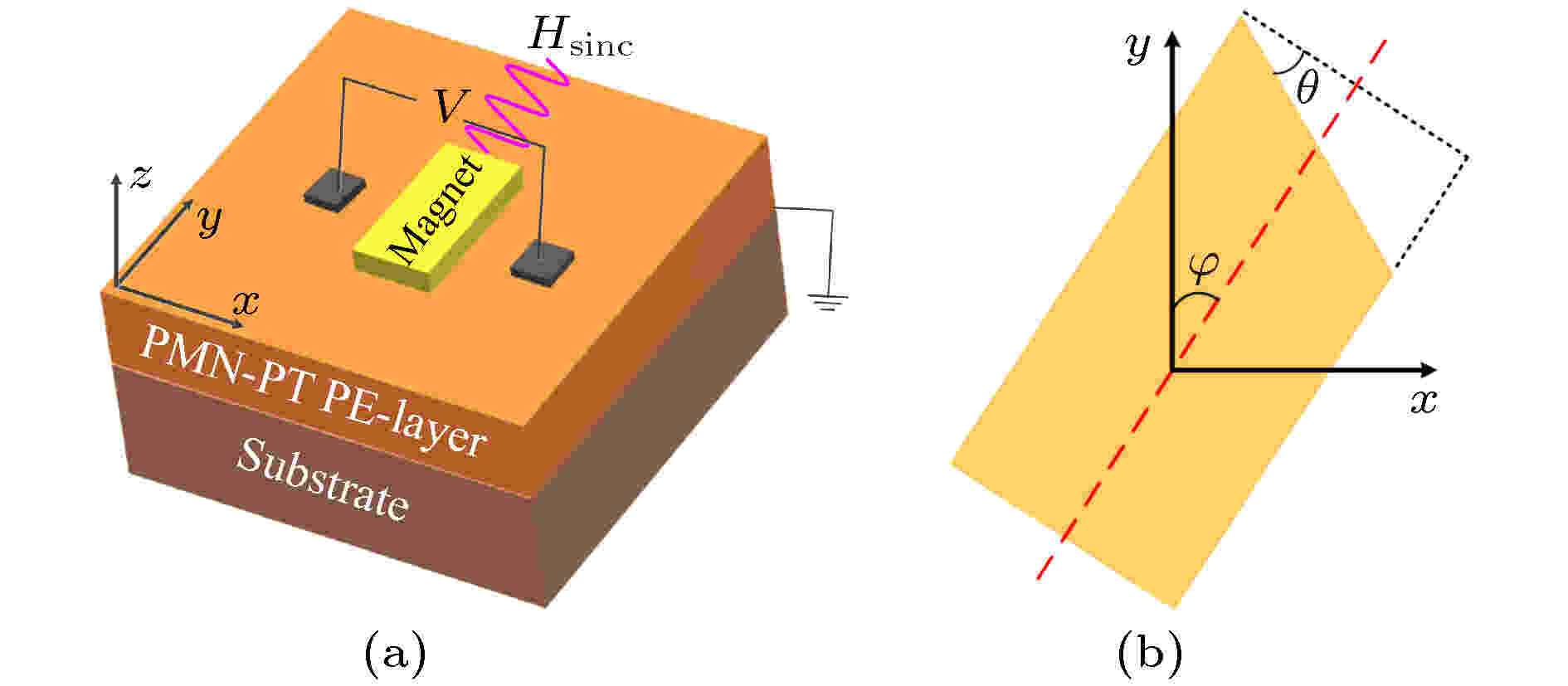
Recently, the operating frequency of nanomagnetic logic device has reached the spin wave frequency of nanomagnets. Therefore, the dynamic magnetic properties of nanomagnets, which are excited by microwave magnetic field, have been explored by many researchers. In this paper, the micro-magnetic model of asymmetric strip nanomagnets under microwave excitation is established. By using the anisotropic stress field (along the x-axis direction) that is generated by a constant voltage and the SINC function microwave magnetic field (along the y-axis direction) to excite the nanomagnets at the same time, the effects of tilt angle and defect angle on the ferromagnetic resonance (FMR) spectrum and spin wave mode of the asymmetric strip nanomagnets are studied. Spectral analysis is performed on the micromagnetic simulation data. Simulation results show that as the tilt angle of the asymmetric strip nanomagnet increases, the ferromagnetic resonance frequency increases. What is more, this phenomenon is independent of the defect angle of the nanomagnet. When the tilt angle is constant, there exists a monotonically increasing relation between the ferromagnetic resonance frequency of the asymmetric strip nanomagnet and the defect angle. The spin wave modes of the nanomagnets differ a lot as defect angle changes. The asymmetric strip nanomagnet is compared with the rectangle nanomagnet, and the spin wave mode of the asymmetric strip nanomagnet is localized. Specifically, the spin wave mode of the asymmetric strip nanomagnets is asymmetric and the high precession region exists at the edge, which is termed asymmetric edge mode. The changes of the tilt angle lead to the changes in the demagnetizing field inside the nanomagnet, which gives rise to the movement of the edge mode. However, the center mode is not sensitive to the change of tilt angle. Finally, the magnetic loss of the model under the excitation of high frequency microwave magnetic field is analyzed and the reliability of the model is verified. These findings indicate that the defect angle and tilt angle can be used to tune the spin wave mode and the ferromagnetic resonance frequency of nanomagnets, and thus providing an important theoretical basis for designing the tunable microwave nanomagnetic devices.

EDITOR'S SUGGESTION
2020, 69 (5): 057502.
doi: 10.7498/aps.69.20191520
Abstract +

2020, 69 (5): 057901.
doi: 10.7498/aps.69.20191891
Abstract +
The wx-AMPS simulation software is used to model and simulate the Schottky perovskite thin film solar cells. The front and back electrodes with different work functions are applied to the Schottky perovskite solar cells to study the effect of band structure on the performance of solar cells. The results show that in a range from 3.8 to 4.4 eV, as the work function of the front electrode decreases, the conversion efficiency of the Schottky solar cells gradually increases. When the work function of the front electrode is low, the electric field strength is large, which facilitates the transport of carriers in the light-absorbing layer of the perovskite and reduces the carrier recombination rate of the perovskite layer. In addition, the recombination ratio of the light absorbing layer is reduced due to the increase of the electric field strength, and the parallel resistance is increased to a certain extent thereby increasing the FF and improving the output efficiency of the battery. At the same time, when the current electrode work function is maintained at 3.8 eV, in a range from 4.3 to 5.5 eV, the higher the work function of the back electrode, the greater the conversion efficiency of the Schottky solar cell is. This conduces to the band alignment in contact between perovskite and back electrode. Under the premise that the common electrode Au is used as a back electrode, the work function of the front electrode is 3.8 eV and the conversion efficiency of the Schottky perovskite solar cell is 17.93%. In addition, by using the optimized front and rear contact electrodes, the quality of the perovskite layer material, thus the performance of the solar cell can be further improved. Doping till a certain concentration and removing the defects of the perovskite layer, the conversion efficiency of the solar cell with a thickness of 500 nm can be increased from 17.93% to 20.1%. The simulation results show that the Schottky perovskite thin film solar cells can obtain excellent performance with simple device structure and have great potential applications.
INTERDISCIPLINARY PHYSICS AND RELATED AREAS OF SCIENCE AND TECHNOLOGY
2020, 69 (5): 058101.
doi: 10.7498/aps.69.20191390
Abstract +
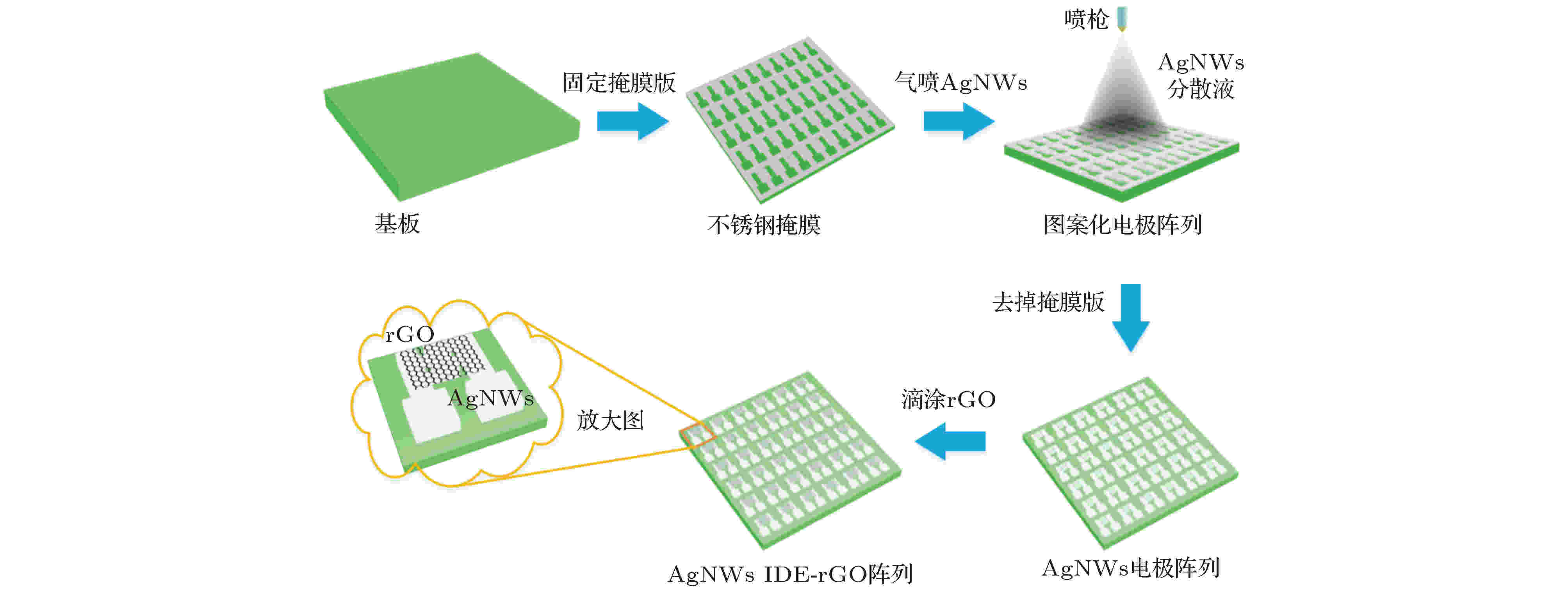
In recent years, flexible gas sensors have aroused wide interest of researchers due to their enormous potential applications in wearable electronic devices. In this paper, a flexible gas sensor is prepared. We use silver nanowires as flexible interdigital electrodes for gas sensors and reduced graphene oxide as gas-sensing materials. We also study its gas sensitivity and flexibility properties such as responsiveness, recovery, and repeatability to nitrogen dioxide. The experimental results show that the silver nanowire flexible electrode and the reduced graphene oxide gas sensor prepared can detect the NO2 gas with a concentration of 5—50 ppm at room temperature. The response (Ra/Rg) of the sensor to 50 ppm NO2 is 1.19. It demonstrates high response ability and repeatability. The recovery rate can be kept above 76%. The sensitivity of the sensor is 0.00281 ppm-1. The response time and recovery time of the prepared AgNWs IDE-rGO sensor for 5 ppm NO2 gas are 990 s and 1566 s, respectively. At the same time, the sensor still exhibits excellent gas sensing performance at a bending angle in range from 0° to 45°. The device has relatively stable conductivity and good bending tolerance. The sensing mechanism of the sensor can be attributed to the direct charge transfer between the reduced graphene oxide material and NO2 gas molecules. In addition, the high catalytic activity and excellent conductivity of Ag that is a common catalyst material, may also play an important role in improving the gas sensitivity of reduced graphene oxide materials. Silver nanowires, as a material for interdigital electrodes, provide excellent conductivity for device as well as support for the flexibility of device. It provides the fabricated sensor for good mechanical flexibility. And the gas-sensing performance of the AgNWs IDE-rGO sensor is mainly achieved by the use of reduced oxidized graphene material reduced by hydrazine hydrate. In summary, the silver nanowire flexible electrode and the graphene gas sensor prepared in this work are helpful in realizing the flexibility of the gas sensor. It lays a foundation for the further application of flexible gas sensors and has great application prospects in wearable electronic equipments.
2020, 69 (5): 058102.
doi: 10.7498/aps.69.20191551
Abstract +
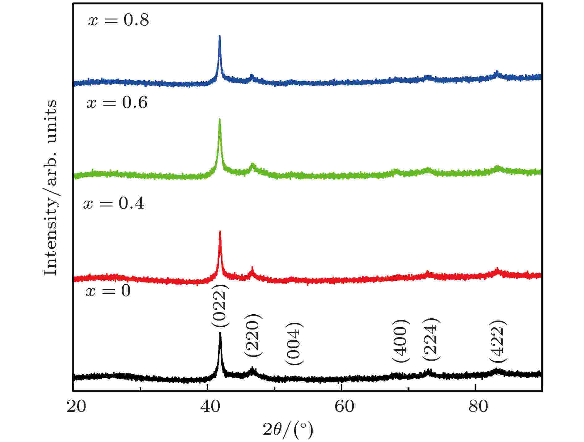
In this paper, phase transformations, magnetic properties and exchange bias of Mn50–xCrxNi42Sn8 (x = 0, 0.4, 0.6, 0.8) polycrystalline samples are investigated. It is found that each of all the alloys has a tetragonal martensite structure at room temperature. The transformation temperature decreases with the increase of Cr content. The maximum magnetization difference between martensite and austenite phase is ∆M = 7.61 emu/g. The change of magnetic properties is mainly related to the change of Mn-Mn distance and the hybridization strength between Ni(A)-Mn(D). The ferromagnetism of martensite can be enhanced by Cr doping. The exchange bias field is observed to reach up to as high as 2624 Oe in Mn50Ni42Sn8 alloy after cooling from room temperature to 5 K in 500 Oe magnetic field, which decreases gradually with the increase of Cr content. Furthermore, the exchange bias field increases first and then followed by a decrease with the increase of the cooling field in Mn49.2Cr0.8Ni42Sn8. This is mainly attributed to the change of the interface exchange coupling between the spin glass state and antiferromagnetic region.
2020, 69 (5): 058103.
doi: 10.7498/aps.69.20191636
Abstract +
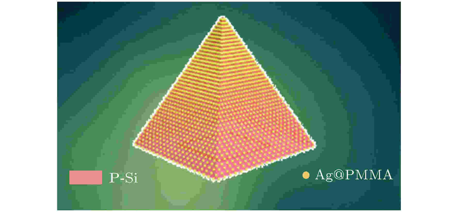
Surface enhanced Raman scattering (SERS) is a highly sensitive spectroscopy technique, which is widely used in chemical reaction detecting, medical diagnostics, and food analysis. The construction of the substrate structure has a very important influence on enhancing the SERS signal of the probe molecule. In this paper, a three-dimensional (3D) pyramid stereo composite SERS substrate is prepared by using polymethyl methacrylate (PMMA) to encapsulate silver nanoparticles, which achieves high sensitivity detection of Rhodamine 6G (R6G) molecules. By adjusting the dispersion density of silver nanoparticles in the PMMA acetone solution, the effective oscillation of light in the pyramid valley is realized, which not only ensures the high-density "hot spot" effect of the 3D structure, but also avoids deforming the adsorption probe molecules caused by the metal-molecule interaction. It also effectively prevents the silver nanoparticles from being oxidized and provides a larger range of electromagnetic enhancement for probe molecules, resulting in a stable output of the enhanced Raman signal. This research result provides an effective strategy for designing a high performance and reusable SERS substrate, meanwhile, it has important guiding significance for further designing an SERS substrate with improved 3D structure in the future study.
GEOPHYSICS, ASTRONOMY, AND ASTROPHYSICS
2020, 69 (5): 059401.
doi: 10.7498/aps.69.20191612
Abstract +
In the last two decades, a wide variety of plasmoids events have been observed, ranging from space and astrophysical phenomenon to magnetically confined laboratory plasmas, in which there are a lot of evidence of observational plasmoid-like features supported by direct large-scaled computer simulations. A super-Alfvénic instability, named plasmoid instability, occurs in an extended current sheet, when the Lundquist number exceeds a critical value. The large-aspect-ratio current sheet is fragmented by generating, growing, coalescing and ejecting of plasmoids so that this phenomenon has been proposed as a possible mechanism for fast reconnection scenario. This super-Alfvénic plasmoid instability has been usedin the significant new development of reconnection theory, and thus can provide alternative and more convincing mechanism for fast reconnection. In this work, a “driving” kind of shear flow in the out-of-plane direction is imposed on a two-dimensional, three-component magnetohydrodynamic model with a current sheet system to study the dynamic process of the plasmoids in a current sheet system. The effect of the width and strength of the driving flow on the reconnection rate of plasmoids are numerically analyzed in detail. It is found that the plasmoids are easily formed in the case of strong and wide out-of-plane driving flow. The reconnection rate and the number of the plasmoids increase with the driving flow width and/or driving flow strength increasing. In the presence of guiding field, it is found that the symmetry of the plasmoids is broken in the reconnection plane. In addition, for the fixed guiding field, the growth rate of plasmoids increases much faster when the strength of driving flow increases.
