


-
通过采用稀土元素镨掺杂铟锡锌氧化物半导体作为薄膜晶体管沟道层, 成功实现了基于铝酸的湿法背沟道刻蚀薄膜晶体管的制备. 研究了N 2O等离子体处理对薄膜晶体管背沟道界面的影响, 对其处理功率和时间对器件性能的影响做了具体研究. 结果表明, 在一定的功率和时间处理下能获得良好的器件性能, 所制备的器件具有良好的正向偏压热稳定性和光照条件下负向偏压热稳定性. 高分辨透射电镜结果显示, 该非晶结构的金属氧化物半导体材料可以有效抵抗铝酸的刻蚀, 未发现明显的成分偏析现象. 进一步的X射线光电能谱测试表明, N 2O等离子体处理能在界面处形成一个富氧、低载流子浓度的界面层. 其一方面可以有效抵抗器件在沉积氧化硅钝化层时等离子体对背沟道的损伤; 另一方面作为氢的钝化体, 抑制了低能级施主态氢的产生, 为低成本、高效的薄膜晶体管性能优化方式提供了重要参考.In this paper, the rare earth element praseodymium-doped indium tin zinc oxide semiconductor is used as the channel layer of the thin film transistor, and the aluminum oxide-based wet back channel etched thin film transistor is successfully prepared. The effect of N 2O plasma treatment on the back-channel interface of thin film transistor is studied, and the effect of treatment power and time on device performance are studied in detail. The results show that the good device performance can be obtained under certain power and time treatment, and the prepared device has good thermal stability of positive bias and negative bias under light conditions. The results from high-resolution transmission electron microscopy show that the amorphous structure of the metal oxide semiconductor material can effectively resist the wet etchant, and that no obvious component segregation phenomenon is found. Further, X-ray photoelectric spectroscopy tests show that N 2O plasma treatment can form an oxygen-rich, low-carrier-concentration interface layer at the interface. On the one hand, it can effectively resist the damage of the back channel caused by the plasma of plasma enhanced chemical vapor deposition (PECVD), and on the other hand, it acts as a passivation body of hydrogen from PECVD plasma, suppressing the generation of low-level donor state of hydrogen. This study provides an important reference for low-cost, high-efficiency thin film transistor performance optimization methods.
-
Keywords:
- metal oxide semiconductor /
- back channel etch /
- thin film transistor /
- N 2O plasma
[1] Nomura K, Ohta H, Takagi A, Kamiya T, Hirano M, Hosono H 2004 Nature 432 488
 Google Scholar
[2] Hoffman R L, Norris B J, Wager J F 2003 Appl. Phys. Lett. 82 733
Google Scholar
[3] 李喜峰, 信恩龙, 石继锋, 陈龙龙, 李春亚, 张建华 2013 物理学报 62 108503
Google Scholar
Li X F, Xin E L, Shi J F, Chen L L, Zhang C Y, ZhangJ H 2013 Acta Phys. Sin. 62 108503
Google Scholar
[4] Fortunato E M C, Barquinha P M C, Pimentel A C M B G, Gonçalves A M F, Marques A J S, Pereira L M N, Martins R F P 2005 Adv. Mater. 17 590
Google Scholar
[5] Chung C Y, Zhu B, Greene R G, Thompson M O, Ast D G 2015 Appl. Phys. Lett. 107 183503
Google Scholar
[6] Song J I, Park J S, Kim H, Heo Y W, Kim G M, Choi B D 2007 Appl. Phys. Lett. 90 022106
Google Scholar
[7] Lan L F, Xiong N N, Xiao P, Li M, Xu H, Yao R H, Wen S S, Peng J B 2013 Appl. Phys. Lett. 102 242102
Google Scholar
[8] Xu H, Xu M, Li M, Chen Z K, Zou J H, Wu W, Qiao X, Tao H, Wang L, Ning H L, Ma D G, Peng J B 2019 ACS Appl. Mater. Interfaces 11 5232
Google Scholar
[9] Kim M, Jeong J H, Lee H J, Ahn T K, Shin H S, Park J, Jeong J K, Mo Y, Kim H D 2007 Appl. Phys. Lett. 90 212114
Google Scholar
[10] Cho S H, Ko J B, Ryu M K, Yang J H, Yeom H I, Lim S K, Hwang C, Park S H K 2015 IEEE Trans. Electron Devices 62 3653
Google Scholar
[11] Park J, Song I, Kim S, Kim S, Kim C, Lee J, Lee H, Lee E, Yin H, Kim K, Kwon K, Park Y 2008 Appl. Phys. Lett. 93 053501
Google Scholar
[12] Xu H, Lan L F, Xu M, Zou J H, Wang L, Wang D, Peng J B 2011 Appl. Phys. Lett. 99 253501
Google Scholar
[13] Ge S M, Li S, Chen S J, Kong X Y, Meng Y H, Shi W, Shi L, Wu W, Liu X, Gan Q, Zhao Y, Zhang C, Chiu C, Lee C Y 2017 SID Symposium Digest of Technical Papers 48 592
Google Scholar
[14] Park J, Kim S, Kim C, Kim S, Song I, Yin H, Kim K, Lee S, Hong K, Lee J, Jung J, Lee E, Kwon K, Park Y 2008 Appl. Phys. Lett. 93 053505
Google Scholar
[15] Tsai C T, Chang T C, Chen S C, Lo I, Tsao S W, Hung M C, Chang J J, Wu C Y, Huang C Y 2010 Appl. Phys. Lett. 96 242105
Google Scholar
[16] Park J C, Ahn S E, Lee H N 2013 ACS Appl. Mater. Interfaces 5 12262
Google Scholar
[17] Sheng J, Park J, Choi D W, Lim J, Park J S 2016 ACS Appl. Mater. Interfaces 8 31136
Google Scholar
[18] Nahm H H, Kim Y S, Kim D H 2012 Phys. Status Solidi B 249 1277
Google Scholar
[19] Zhu Y B, Xu H, Xu M, Li M, Zou J H, Tao H, Wang L, Peng J B 2021 Phys. Status Solidi A doi: 10.1002/pssa.202000812
[20] 朱宇博, 徐华, 李民, 徐苗, 彭俊彪 2021 物理学报 70 168501
Google Scholar
Zhu Y B, Xu H, Li M, Xu M, Peng J B 2021 Acta Phys. Sin. 70 168501
Google Scholar
[21] Fortunato E, Barquinha P, Martins R 2012 Adv. Mater. 24 2945
Google Scholar
[22] Ide K, Nomura K, Hosono H, Kamiya T 2019 Phys. Status Solidi A 216 1800372
Google Scholar
[23] Remashan K, Hwang D K, Park S D, Bae J W, Yeom G Y, Park S J, Jang J H 2007 Electrochem. Solid State Lett. 11 H55
[24] Kang Y, Ahn B D, Song J H, Mo Y G, Nahm H H, Han S, Jeong J K 2015 Adv. Electron. Mater. 1 1400006
Google Scholar
[25] Son K S, Kim T S, Jung J S, Ryu M K, Park K B, Yoo B W, Park K C, Kwon J Y, Lee S Y, Kim J M 2008 Electrochem. Solid State Lett. 12 H26
-

图 1 PITZO-TFT (a)结构示意图; (b) 器件显微镜照片
Fig. 1. (a) Structure diagram and (b) microscope photo of the PITZO-TFT.
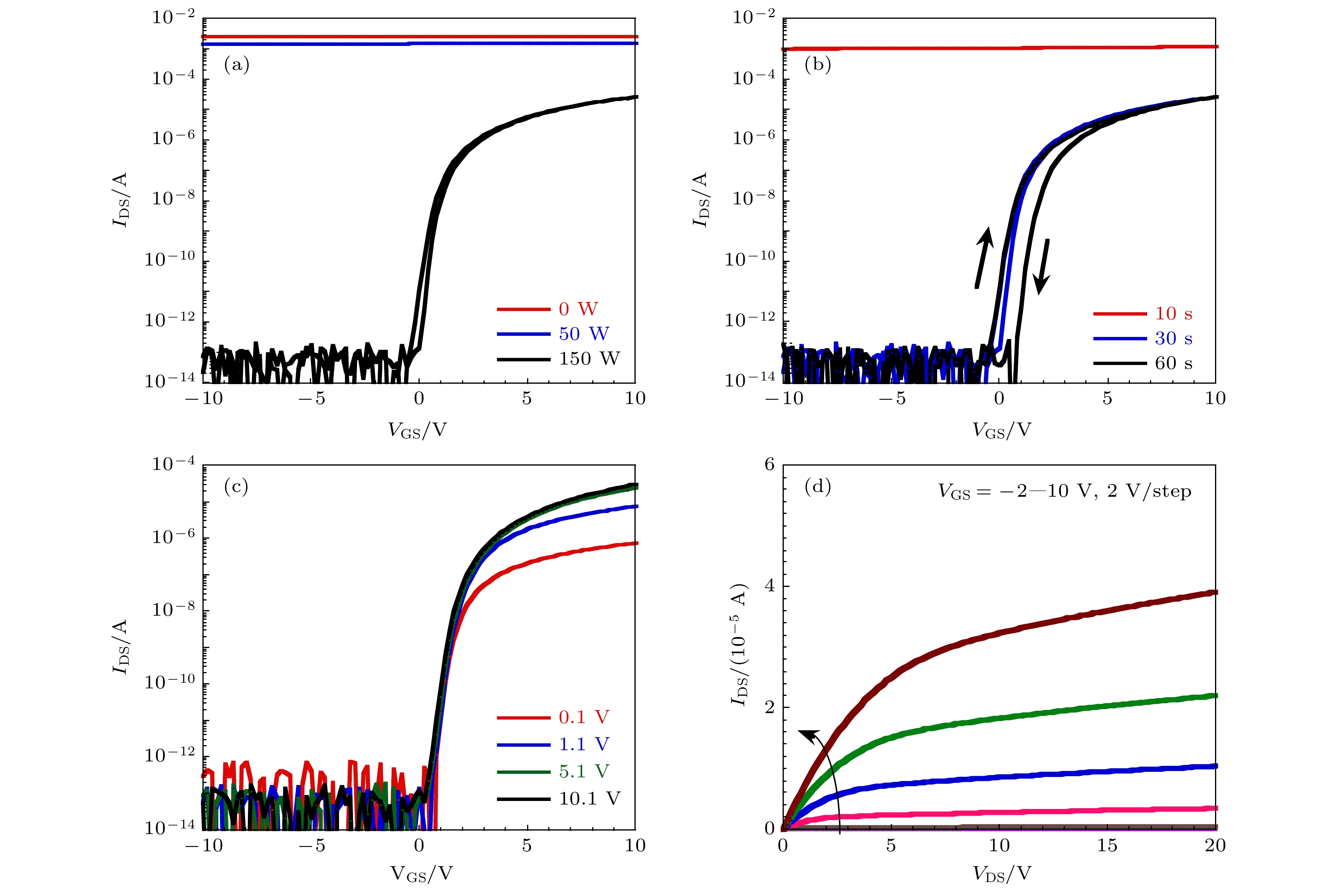
图 2 (a)不同功率和 (b) 不同时间的N 2O处理对器件转移特性的影响; Device C (c) 不同源漏电压下的转移特性曲线和 (d) 输出特性曲线
Fig. 2. Influence of different (a) power and (b) time treatment of N 2O on the transfer characteristics of the device; (c) transfer characteristic curve under different source and drain voltages and (d) output characteristic curve of Device C.

图 3 (a) Device C和 (b) Device E 器件在PBTS条件下的稳定性; (c) Device C和 (d) Device E 器件在NBITS条件下的稳定性
Fig. 3. Stability of (a) Device C and (b) Device E under PBTS conditions; stability of (c) Device C and (d) Device E under NBITS conditions.

图 4 TFT器件的高分辨透射电镜谱图
Fig. 4. High-resolution transmission electron microscope spectra of TFT devices.
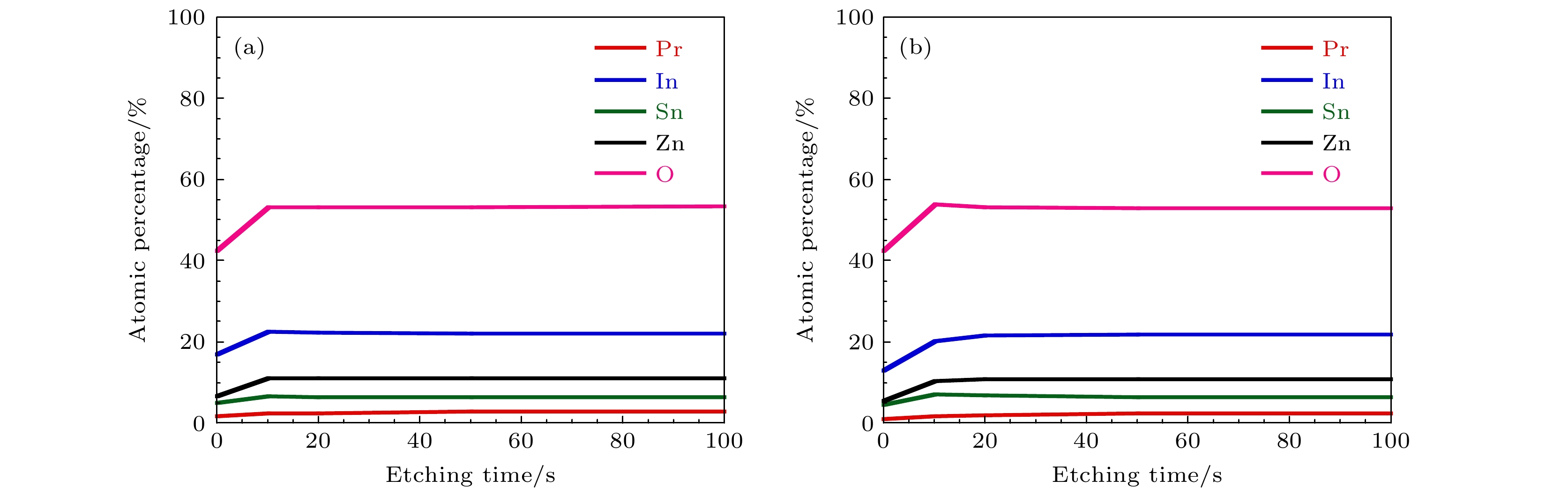
图 5 PITZO薄膜的深度剖析X射线光电子能谱图 (a) 无N 2O处理; (b) N 2O处理后
Fig. 5. X-ray photoelectron spectroscopy depth-profile of PITZO films: (a) Without N 2O treatment; (b) with N 2O treatment.
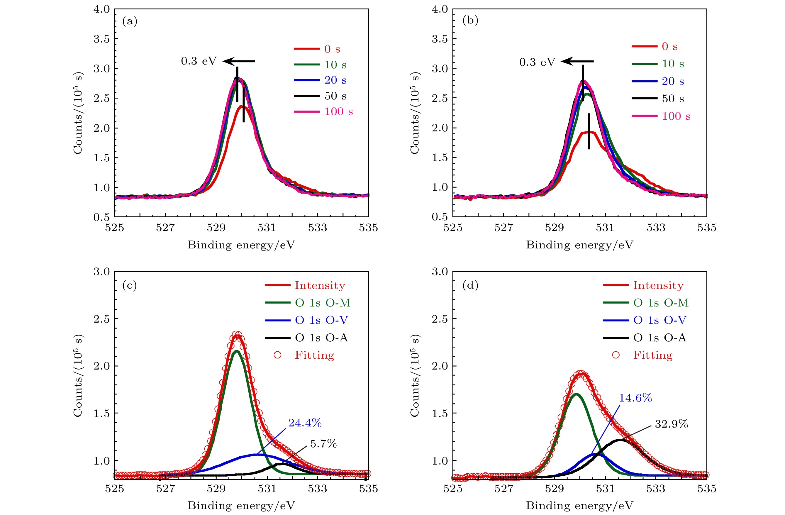
图 6 PITZO薄膜在 (a) 无N 2O处理和 (b) N 2O处理后O 1s的XPS谱图随刻蚀时间的关系; Ar离子枪刻蚀前 (c) 无N 2O处理和 (d) N 2O处理后薄膜O 1s的拟合XPS图谱
Fig. 6. The O 1s XPS spectra of the PITZO films (a) without N 2O and (b) with N 2O treatment related with the Ar ion gun etching time. Fitted O 1s XPS of the PITZO thin films (c) without N 2O and (d) with N 2O treatment before Ar ion gun etching.
表 1 各器件性能参数表
Table 1. Electronic parameters of each TFTs.
No. V th/V μ sat/(cm 2·V –1·s –1) SS/(V·decade –1) I on- I off Device A — — — — Device B — — — — Device C 0.7 22.4 0.17 10 8 Device D — — — — Device E 0.4 20.6 0.22 10 8  下载: 导出CSV
-
[1] Nomura K, Ohta H, Takagi A, Kamiya T, Hirano M, Hosono H 2004 Nature 432 488
Google Scholar
[2] Hoffman R L, Norris B J, Wager J F 2003 Appl. Phys. Lett. 82 733
Google Scholar
[3] 李喜峰, 信恩龙, 石继锋, 陈龙龙, 李春亚, 张建华 2013 物理学报 62 108503
Google Scholar
Li X F, Xin E L, Shi J F, Chen L L, Zhang C Y, ZhangJ H 2013 Acta Phys. Sin. 62 108503
Google Scholar
[4] Fortunato E M C, Barquinha P M C, Pimentel A C M B G, Gonçalves A M F, Marques A J S, Pereira L M N, Martins R F P 2005 Adv. Mater. 17 590
Google Scholar
[5] Chung C Y, Zhu B, Greene R G, Thompson M O, Ast D G 2015 Appl. Phys. Lett. 107 183503
Google Scholar
[6] Song J I, Park J S, Kim H, Heo Y W, Kim G M, Choi B D 2007 Appl. Phys. Lett. 90 022106
Google Scholar
[7] Lan L F, Xiong N N, Xiao P, Li M, Xu H, Yao R H, Wen S S, Peng J B 2013 Appl. Phys. Lett. 102 242102
Google Scholar
[8] Xu H, Xu M, Li M, Chen Z K, Zou J H, Wu W, Qiao X, Tao H, Wang L, Ning H L, Ma D G, Peng J B 2019 ACS Appl. Mater. Interfaces 11 5232
Google Scholar
[9] Kim M, Jeong J H, Lee H J, Ahn T K, Shin H S, Park J, Jeong J K, Mo Y, Kim H D 2007 Appl. Phys. Lett. 90 212114
Google Scholar
[10] Cho S H, Ko J B, Ryu M K, Yang J H, Yeom H I, Lim S K, Hwang C, Park S H K 2015 IEEE Trans. Electron Devices 62 3653
Google Scholar
[11] Park J, Song I, Kim S, Kim S, Kim C, Lee J, Lee H, Lee E, Yin H, Kim K, Kwon K, Park Y 2008 Appl. Phys. Lett. 93 053501
Google Scholar
[12] Xu H, Lan L F, Xu M, Zou J H, Wang L, Wang D, Peng J B 2011 Appl. Phys. Lett. 99 253501
Google Scholar
[13] Ge S M, Li S, Chen S J, Kong X Y, Meng Y H, Shi W, Shi L, Wu W, Liu X, Gan Q, Zhao Y, Zhang C, Chiu C, Lee C Y 2017 SID Symposium Digest of Technical Papers 48 592
Google Scholar
[14] Park J, Kim S, Kim C, Kim S, Song I, Yin H, Kim K, Lee S, Hong K, Lee J, Jung J, Lee E, Kwon K, Park Y 2008 Appl. Phys. Lett. 93 053505
Google Scholar
[15] Tsai C T, Chang T C, Chen S C, Lo I, Tsao S W, Hung M C, Chang J J, Wu C Y, Huang C Y 2010 Appl. Phys. Lett. 96 242105
Google Scholar
[16] Park J C, Ahn S E, Lee H N 2013 ACS Appl. Mater. Interfaces 5 12262
Google Scholar
[17] Sheng J, Park J, Choi D W, Lim J, Park J S 2016 ACS Appl. Mater. Interfaces 8 31136
Google Scholar
[18] Nahm H H, Kim Y S, Kim D H 2012 Phys. Status Solidi B 249 1277
Google Scholar
[19] Zhu Y B, Xu H, Xu M, Li M, Zou J H, Tao H, Wang L, Peng J B 2021 Phys. Status Solidi A doi: 10.1002/pssa.202000812
[20] 朱宇博, 徐华, 李民, 徐苗, 彭俊彪 2021 物理学报 70 168501
Google Scholar
Zhu Y B, Xu H, Li M, Xu M, Peng J B 2021 Acta Phys. Sin. 70 168501
Google Scholar
[21] Fortunato E, Barquinha P, Martins R 2012 Adv. Mater. 24 2945
Google Scholar
[22] Ide K, Nomura K, Hosono H, Kamiya T 2019 Phys. Status Solidi A 216 1800372
Google Scholar
[23] Remashan K, Hwang D K, Park S D, Bae J W, Yeom G Y, Park S J, Jang J H 2007 Electrochem. Solid State Lett. 11 H55
[24] Kang Y, Ahn B D, Song J H, Mo Y G, Nahm H H, Han S, Jeong J K 2015 Adv. Electron. Mater. 1 1400006
Google Scholar
[25] Son K S, Kim T S, Jung J S, Ryu M K, Park K B, Yoo B W, Park K C, Kwon J Y, Lee S Y, Kim J M 2008 Electrochem. Solid State Lett. 12 H26

 下载:
下载:
计量
- 文章访问数: 6090
- PDF下载量: 103
- 被引次数: 0
