-
通过第一原理电子结构计算来研究有序多孔纳米网的电导特性变化的能带机理. 能带结构分析结果表明: 石墨烯纳米网超晶格(3m, 3n)(m和n为整数)的电子本征态在布里渊区中心点发生四重简并; 碳空位孔洞规则排列形成的石墨烯纳米网具有由简并态分裂形成的宽度可调带隙, 无论石墨烯的两个子晶格是否对等. 在具有磁性网孔阵列的石墨烯纳米网中, 反铁磁耦合使对称子晶格的反演对称性增加了一项量子限制条件, 导致能带结构在 K 点的二重简并态分裂成带隙. 通过控制网孔密度能够有效调节石墨烯纳米网的带隙宽度, 为实现新一代石墨烯纳米电子器件提供了理论依据.By means of first-principles electronic structure calculations, the ordered graphene nanomeshes with patterned hexagonal vacancy holes are theoretically studied to explore the modification mechanism of electrical conduction on graphene atomic monolayers. According to pseudopotential plane wave first-principles scheme based on density functional theory, the band structures of graphene nanomeshes are calculated to analyze the electrical conductance in correlation with the superlattice symmetry and vacancy hole magnetism. Based on the structural features and topological magnetism of Y-shaped nodes between the nanopores on the atomic monolayer of graphene, the graphene nanomeshes are classified into three types. The quadruplet degeneracy and splitting of electronic states at Brillouin zone center are investigated by comparing the band structures of graphene nanomeshes and analogical superlattices. The effects of inversion symmetry and supercell size on the opening band-gap at Dirac cone are elaborately analyzed with the consideration of antiferromagnetic coupling and hydrogen passivation at the magnetic edge of nanopores on graphene nanomeshes. The band-structure calculation results indicate that the (3m, 3n) (m and n are integers) superlattices have fourfold degenerate electronic states at center point of Brillouin zone, which can be effectively splitted by regularly arranging porous atomic vacancy to make the (3m, 3n) nanomesh, resulting in adjustable band-gap no matter whether or not the sublattices keeping in equivalence. In the nanomeshes formed by patterned holes with magnetic edge, the antiferromagnetic coupling adds a quantum parameter to the inversion symmetry so as to break the sublattice equivalence, opening band-gap at the twofold degenerate K point. Nevertheless, the hydrogen passivation at the edge of magnetic nanopores will convert the magnetic graphene nanomeshes into non-magnetic and eliminate the band-gap at K point. The band-gap of graphene nanomeshes could also be controlled by changing the density of nanopores, suggesting a graphene nanomaterial with adjustable band-gap that can be designed by controlling the mesh pore spacing. The graphene nanomeshes represent a new mechanism of forming band-gap and thus promise a strategy for achieving special electrical properties of graphene nanostructures. These results also theoretically demonstrate that the nano-graphene is a prospective candidate with flexibly adjustable electrical properties for realizing multivariate applications in new-generation nano-electronics.
-
Keywords:
- graphene nanomesh /
- electronic structure /
- first-principles calculation /
- conduction property
[1] Pakhira S, Mendoza-Cortes J L 2018 J. Phys. Chem. C 122 4768
[2] Novoselov K S, Geim A K, Morozov S V, Jiang D, Katsnelson M I, Grigorieva I V, Dubonos S V, Firsov A A 2005 Nature 438 197
 Google Scholar
[3] Long M Q, Tang L, Wang D, Wang L J, Shuai Z 2009 J. Am. Chem. Soc. 131 17728
 Google Scholar
[4] Zhang J, Li V, Ji W X, Zhang C W, Li P, Zhang S F, Wang P J, Yan S S 2017 J. Mater. Chem. C 5 8847
[5] Dong Y F, Liu P G, Yin W Y, Li G S, Yi B 2015 Physica E 70 176
 Google Scholar
[6] Zhou J, Liang Q F, Dong J M 2010 Carbon 48 1405
 Google Scholar
[7] Tang G, Zhang Z, Deng X, Fan Z, Zeng Y, Zhou J 2014 Carbon 76 348
 Google Scholar
[8] Wang S F, Chen L Y, Zhang J M 2017 Superlattice. Microst. 104 341
 Google Scholar
[9] Eldeeb M S, Fadlallah M M, Martyna G J, Maarouf A A 2018 Carbon 133 369
 Google Scholar
[10] Jangid P, Pathan D, Kottantharayil A 2018 Carbon 132 65
 Google Scholar
[11] Pardini L, Löffler S, Biddau G, Hambach R, Kaiser U, Draxl C, Schattschneider P 2016 Phys. Rev. Lett. 117 036801
 Google Scholar
[12] Ouyang F, Yang Z, Peng S, Zheng X, Xiong X 2014 Physica E 56 222
 Google Scholar
[13] Sheu S Y, Yang D Y 2014 Carbon 71 76
 Google Scholar
[14] Shohany B G, Roknabadi M R, Kompany A 2018 Comp. Mater. Sci. 144 280
 Google Scholar
[15] Wang T H, Zhu Y F, Jiang Q 2014 Carbon 77 431
 Google Scholar
[16] Yang C K 2010 Carbon 48 3901
 Google Scholar
[17] Takahashi T, Sugawara K, Noguchi E, Sato T, Takahashi T 2014 Carbon 73 141
 Google Scholar
[18] Lu Y H, Chen W, Feng Y P 2009 J. Phys. Chem. B 113 2
[19] Kheirabadi N, Shafiekhani A 2013 Physica E 47 309
 Google Scholar
[20] Ajeel F N, Mohammed M H, Khudhair A M 2019 Physica E 105 105
 Google Scholar
[21] Mohammed M H 2018 Physica E 95 86
 Google Scholar
[22] Xiu S L, Zheng M M, Zhao P, Zhang Y, Liu H Y, Li S J, Chen G, Kawazoe Y 2014 Carbon 79 646
 Google Scholar
[23] Sandner A, Preis T, Schell C, Giudici P, Watanabe K, Taniguchi T, Weiss D, Eroms J 2015 Nano Lett. 15 8402
 Google Scholar
[24] Liu L Z, Tian S B, Long Y Z, Li W X, Yang H F, Li J J, Gu C Z 2014 Vacuum 105 21
 Google Scholar
[25] Şahin H, Ciraci S 2011 Phys. Rev. B 84 035452
 Google Scholar
[26] Liang X G, Jung Y S, Wu S W, Ismach A, Olynick D L, Cabrini S, Bokor J 2010 Nano Lett. 10 2454
 Google Scholar
[27] Yang W, Lu X B, Chen G R, Wu S, Xie G B, Cheng M, Wang D M, Yang R, Shi D G, Watanabe K, Taniguchi T, Voisin C, Placais B, Zhang Y B, Zhang G Y 2016 Nano Lett. 16 2387
 Google Scholar
[28] Molina-Valdovinos S, Martinez-Riveraa J, Moreno-Cabreraa N E, Rodriguez-Vargas I 2018 Physica E 101 188
 Google Scholar
[29] Kress G, Furthmüller J 1996 Phys. Rev. B 54 11169
 Google Scholar
[30] Perdew J P, Ruzsinszky A, Csonka G I, Vydrov O A, Scuseria G E, Constantin L A, Zhou X L, Burke K 2008 Phys. Rev. Lett. 100 136406
 Google Scholar
[31] Kress G, Joubert D 1999 Phys. Rev. B 59 1758
[32] Pfrommer B G, Co te, Louie S G, Cohen M L 1997 J. Comput. Phys. 131 233
 Google Scholar
-
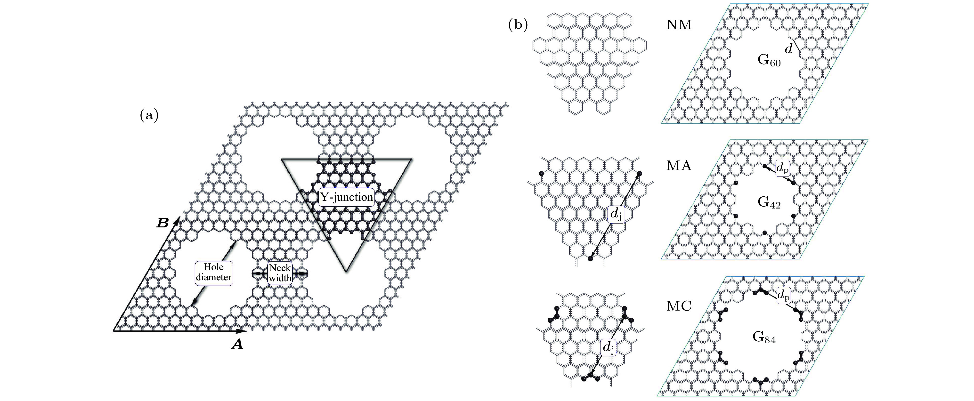
图 1 (a) 网孔周期性有序排列的石墨烯纳米网示意图; (b) 不同磁分布的三种类型石墨烯纳米网的空孔超晶格胞结构(左)和Y形结点连接部分(右), 黑色小球表示G42 (MA) 和G84 (MC) 网孔边缘上具有净自旋磁矩分布的碳原子
Fig. 1. (a) Schematic structure of graphene nanomesh with periodically patterned holes; (b) the supperlattice cells (left) and Y-junction connection areas (right) for three types of vacant holes with different magnetic distributions, black beads represent carbon atoms distributed with net spin moment at the edge of G42 (MA) and G84 (MC) holes in graphene nanomeshes.
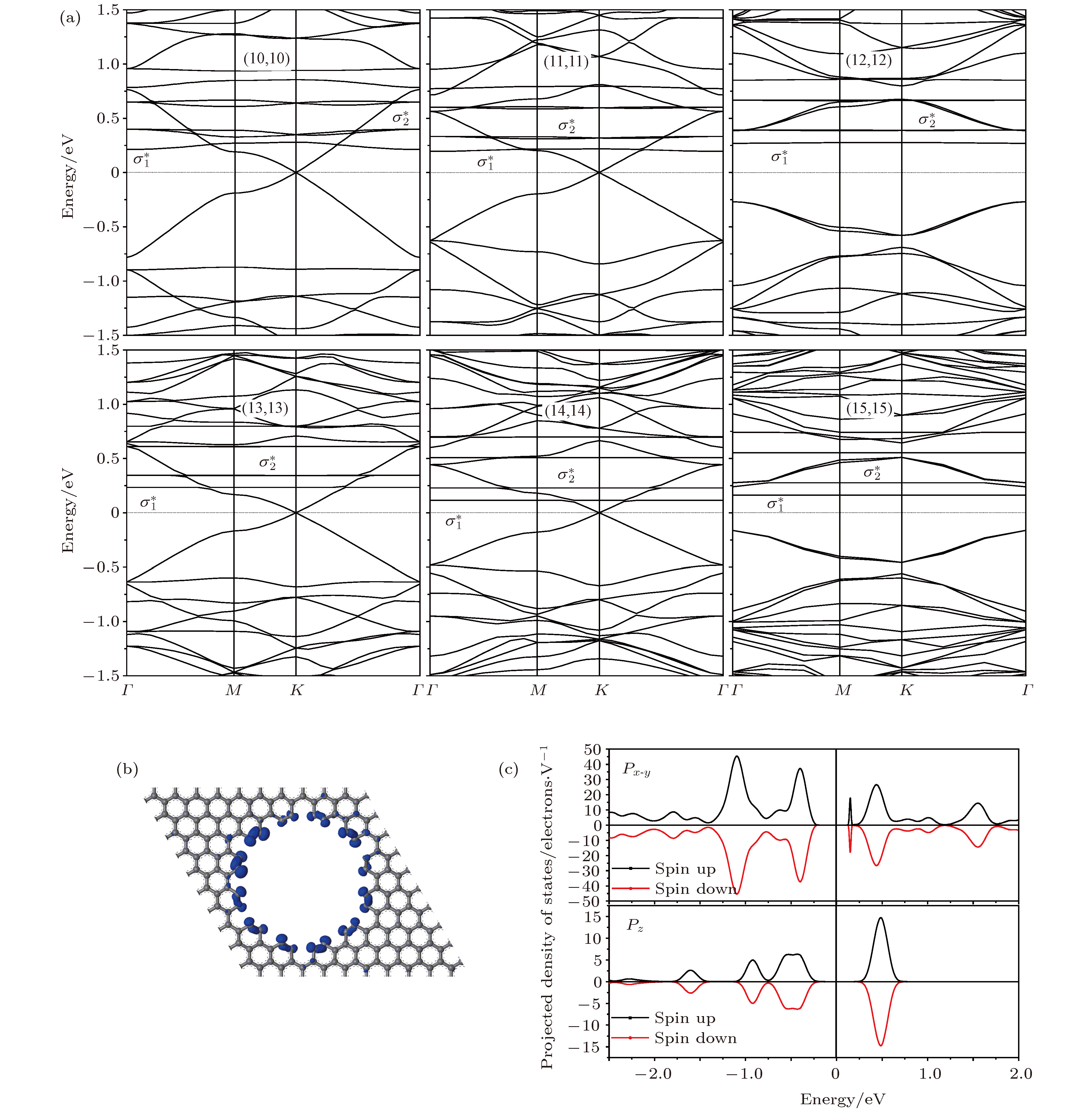
图 2 G60石墨烯纳米网的电子结构计算结果 (a)超晶格(N, N)胞尺寸N = 10 – 15的G60纳米网能带结构; (b) N = 12的G60纳米网在布里渊区K点σ*态的电子密度空间分布(电子态能量~0.2 eV); (c) N = 12网孔边缘碳原子的投影能态密度. 费米能级为参考能量零点(竖直虚线)
Fig. 2. Calculated electronic structures of G60 patterned graphene nanomeshes: (a) Energy band structures of the G60 nanomeshes with supplattice cell (N, N) (N = 10 – 15); (b) the electron density distribution of the σ* state at K point in the energy ~0.2 eV for N = 12; (c) the projected density of states on the carbon atoms of hole edge for N = 12. The reference energy zero is set as Fermi energy level indicated with horizontal dot line.
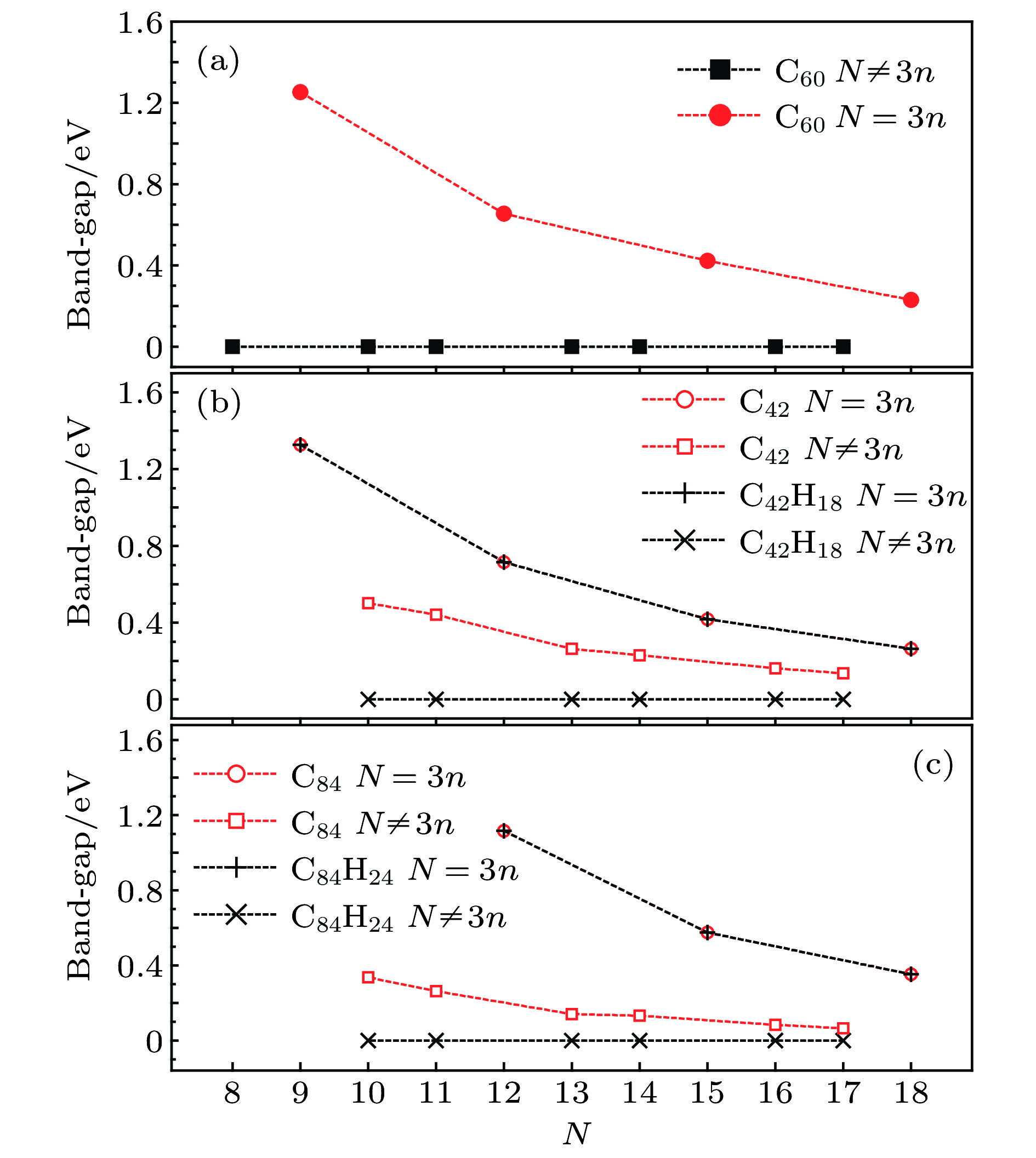
图 4 G60 (N, N)石墨烯纳米网的网孔边缘碳-碳原子间距d (a)以及σ*态的K点能级(b)随超晶格胞尺寸N的变化, 费米能级作为参考能量零点
Fig. 4. Carbon-carbon atomic distance d at hole edge (a) and energy level of the σ* state at K point (b) as a function of supperlattice cell size N for the G60 (N, N) graphene nanomeshes, with Fermi energy level referenced as energy zero.
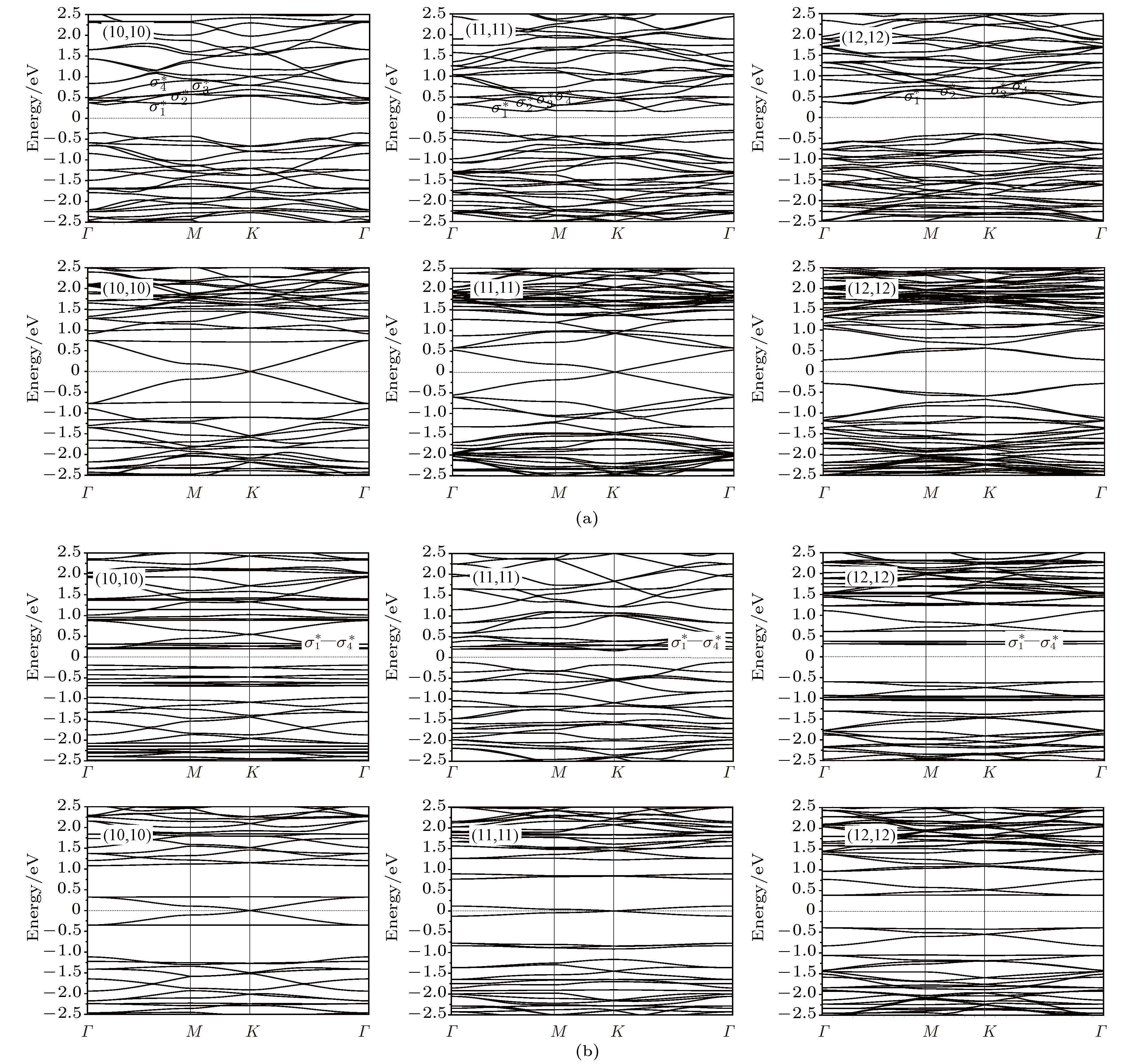
图 5 (a) MA (G42)和(b) MC (G84)型网孔石墨烯纳米网的能带结构, 上下两行能带结构图分别对应网孔边缘碳原子无氢钝化和氢钝化的石墨烯纳米网
Fig. 5. Energy band structures of the graphene nanomeshes with (a) MA (G42) and (b) MC (G84) patterned holes, respectively. The up and down panels represent nanomeshes without and with hydrogen passivation at hole edge, respectively.
-
[1] Pakhira S, Mendoza-Cortes J L 2018 J. Phys. Chem. C 122 4768
[2] Novoselov K S, Geim A K, Morozov S V, Jiang D, Katsnelson M I, Grigorieva I V, Dubonos S V, Firsov A A 2005 Nature 438 197
 Google Scholar
[3] Long M Q, Tang L, Wang D, Wang L J, Shuai Z 2009 J. Am. Chem. Soc. 131 17728
 Google Scholar
[4] Zhang J, Li V, Ji W X, Zhang C W, Li P, Zhang S F, Wang P J, Yan S S 2017 J. Mater. Chem. C 5 8847
[5] Dong Y F, Liu P G, Yin W Y, Li G S, Yi B 2015 Physica E 70 176
 Google Scholar
[6] Zhou J, Liang Q F, Dong J M 2010 Carbon 48 1405
 Google Scholar
[7] Tang G, Zhang Z, Deng X, Fan Z, Zeng Y, Zhou J 2014 Carbon 76 348
 Google Scholar
[8] Wang S F, Chen L Y, Zhang J M 2017 Superlattice. Microst. 104 341
 Google Scholar
[9] Eldeeb M S, Fadlallah M M, Martyna G J, Maarouf A A 2018 Carbon 133 369
 Google Scholar
[10] Jangid P, Pathan D, Kottantharayil A 2018 Carbon 132 65
 Google Scholar
[11] Pardini L, Löffler S, Biddau G, Hambach R, Kaiser U, Draxl C, Schattschneider P 2016 Phys. Rev. Lett. 117 036801
 Google Scholar
[12] Ouyang F, Yang Z, Peng S, Zheng X, Xiong X 2014 Physica E 56 222
 Google Scholar
[13] Sheu S Y, Yang D Y 2014 Carbon 71 76
 Google Scholar
[14] Shohany B G, Roknabadi M R, Kompany A 2018 Comp. Mater. Sci. 144 280
 Google Scholar
[15] Wang T H, Zhu Y F, Jiang Q 2014 Carbon 77 431
 Google Scholar
[16] Yang C K 2010 Carbon 48 3901
 Google Scholar
[17] Takahashi T, Sugawara K, Noguchi E, Sato T, Takahashi T 2014 Carbon 73 141
 Google Scholar
[18] Lu Y H, Chen W, Feng Y P 2009 J. Phys. Chem. B 113 2
[19] Kheirabadi N, Shafiekhani A 2013 Physica E 47 309
 Google Scholar
[20] Ajeel F N, Mohammed M H, Khudhair A M 2019 Physica E 105 105
 Google Scholar
[21] Mohammed M H 2018 Physica E 95 86
 Google Scholar
[22] Xiu S L, Zheng M M, Zhao P, Zhang Y, Liu H Y, Li S J, Chen G, Kawazoe Y 2014 Carbon 79 646
 Google Scholar
[23] Sandner A, Preis T, Schell C, Giudici P, Watanabe K, Taniguchi T, Weiss D, Eroms J 2015 Nano Lett. 15 8402
 Google Scholar
[24] Liu L Z, Tian S B, Long Y Z, Li W X, Yang H F, Li J J, Gu C Z 2014 Vacuum 105 21
 Google Scholar
[25] Şahin H, Ciraci S 2011 Phys. Rev. B 84 035452
 Google Scholar
[26] Liang X G, Jung Y S, Wu S W, Ismach A, Olynick D L, Cabrini S, Bokor J 2010 Nano Lett. 10 2454
 Google Scholar
[27] Yang W, Lu X B, Chen G R, Wu S, Xie G B, Cheng M, Wang D M, Yang R, Shi D G, Watanabe K, Taniguchi T, Voisin C, Placais B, Zhang Y B, Zhang G Y 2016 Nano Lett. 16 2387
 Google Scholar
[28] Molina-Valdovinos S, Martinez-Riveraa J, Moreno-Cabreraa N E, Rodriguez-Vargas I 2018 Physica E 101 188
 Google Scholar
[29] Kress G, Furthmüller J 1996 Phys. Rev. B 54 11169
 Google Scholar
[30] Perdew J P, Ruzsinszky A, Csonka G I, Vydrov O A, Scuseria G E, Constantin L A, Zhou X L, Burke K 2008 Phys. Rev. Lett. 100 136406
 Google Scholar
[31] Kress G, Joubert D 1999 Phys. Rev. B 59 1758
[32] Pfrommer B G, Co te, Louie S G, Cohen M L 1997 J. Comput. Phys. 131 233
 Google Scholar
计量
- 文章访问数: 14780
- PDF下载量: 216
- 被引次数: 0


 下载:
下载:


