-
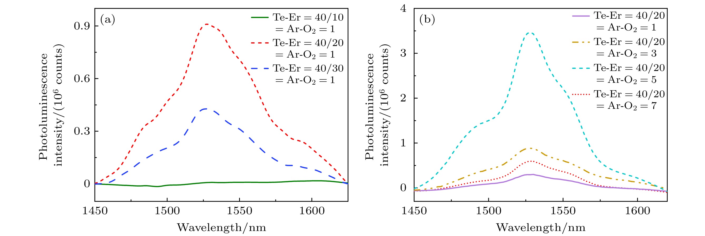
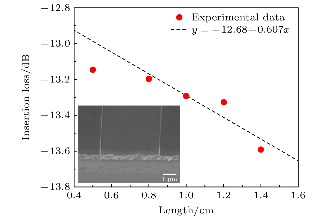
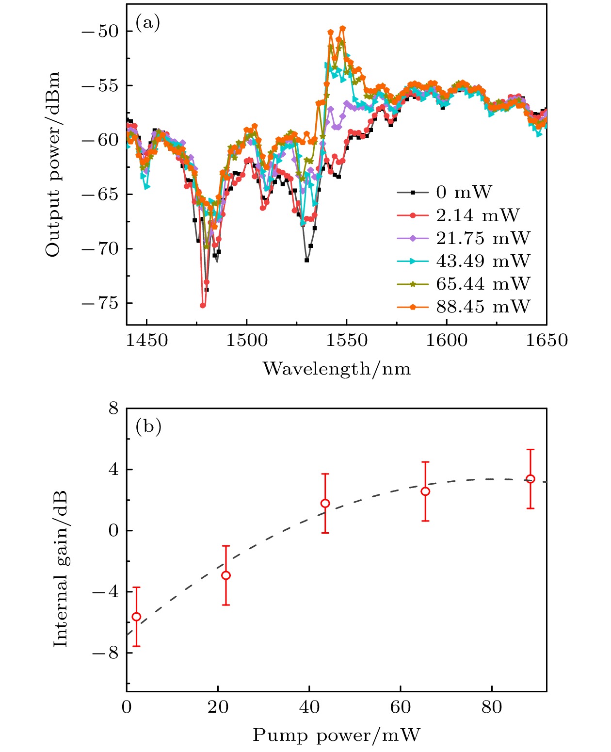
利用射频磁控溅射法制备了掺铒TeO2薄膜, 探究了氧化铒靶溅射功率、Ar/O2气体比例以及退火温度对薄膜发光特性的影响. 实验结果表明, 在氧化铒靶溅射功率为20 W、Ar/O2气体流量比为5∶1、退火温度250 ℃时, 薄膜呈现出良好的光致发光性能. 针对直接刻蚀掺铒薄膜层易引发表面粗糙等问题, 设计并采用紫外光刻和等离子体刻蚀工艺制备了双层波导结构. 使用截断法测得0.5 cm长的掺铒TeO2波导在1310 nm波长处的最低光学损耗为0.607 dB/cm, 放大性能测量表明在1545 nm波段, 波导具有7.2 dB/cm的光学内增益. 这些实验结果表明, 掺铒TeO2波导在平面集成波导放大器领域极具应用潜力.The rapid advancement of information technology has sparked an exponential demand for high-speed, large-capacity data transmission and processing. Traditional electronic communication systems face inherent limitations such as bandwidth constraints and electromagnetic interference, prompting people to shift toward photonic technologies. Integrated optical waveguides, as core components of on-chip photonic systems, enable efficient light confinement and manipulation at microscale dimensions, offering advantages in miniaturization, low power consumption, and high compatibility with existing optical communication infrastructure. Among these, erbium-doped waveguide amplifiers (EDWAs) have emerged as critical active devices for signal amplification in the 1550 nm communication band, leveraging the radiative transitions of Er3+ ions to achieve optical gain. Numerous studies have shown that the fluorescence performance of Er3+ is closely related to the factors such as doping method, preparation and annealing conditions. Besides, the performance of such amplifiers heavily relies on the choice of host materials, which must exhibit low optical loss, high rare-earth ion solubility, and compatibility with complementary metal-oxide-semiconductor (CMOS) fabrication processes. Tellurium dioxide (TeO2), with its high refractive index (2.1–2.4), broad transparency range (0.33–5 μm), exceptional chemical stability, and low phonon energy, has shown significant promise as a superior alternative to traditional materials such as silicon nitride (Si3N4) and aluminum oxide (Al2O3). This study focuses on the development of erbium-doped TeO2 (Er:TeO2) ridge waveguides for on-chip optical amplification. The Er:TeO2 thin films are deposited via radio frequency (RF) magnetron sputtering using high-purity Te and Er targets. The key deposition parameters, including Er2O3 target sputtering power (10–30 W), Ar/O2 gas flow ratio (1∶1 to 5∶1), and post-deposition annealing conditions (200–300 ℃ under oxygen atmosphere), are systematically optimized to improve photoluminescence properties. Scanning electron microscopy (SEM) and fluorescence spectroscopy are employed to evaluate film morphology and emission characteristics. A bilayer waveguide structure is designed to mitigate surface roughness induced by direct etching of the Er-doped layer. The lower Er:TeO2 active layer (500 nm in thickness) and upper undoped TeO2 cladding layer (150 nm in thickness) are patterned by using ultraviolet lithography and plasma etching (O2/Ar/CHF3 gas mixture), achieving a ridge width of 2 μm. Optical confinement and mode field distribution are simulated by using finite-difference eigenmode (FDE) analysis, confirming effective light-matter overlap within the Er-doped region. Experimental results reveal that the optimal Er:TeO2 film, deposited at an Er target power of 20 W and an Ar/O2 flow ratio of 5∶1, and annealed at 250 ℃ for 10 hours, exhibits a photoluminescence intensity of 3.5 × 10⁶ photon counts at 1545 nm–nearly two orders of magnitude higher than non-annealed samples. Oxygen annealing effectively activates Er3+ ions while passivating oxygen vacancies, which is critical for minimizing non-radiative recombination. Excessive Er doping (30 W in sputtering power) leads to ion clustering and fluorescence quenching, highlighting the importance of controlled dopant concentration. Surface morphology analysis via SEM and optical microscopy confirms smooth, crack-free films with minimal particulate contamination, which is essential for low-loss waveguide fabrication. Waveguide performance is characterized by using the cut-back method at 1310 nm, yielding a propagation loss of 0.607 dB/cm for a 0.5 cm-long device. However, a coupling loss of 6.34 dB/facet is observed due to rough end-faces from mechanical dicing, highlighting the need for post-fabrication polishing or anti-reflective coatings. Amplification tests at 1545 nm under 980 nm pumping demonstrate an internal gain of 7.2 dB/cm at a pump power of 88.45 mW, with gain saturation observed beyond 90 mW. The broadband emission spectrum (80 nm full-width at half-maximum) further validates Er:TeO2’s potential for wideband amplification in the C-bands. In summary, this study elucidates the advantages of erbium-doped tellurium oxide (Er:TeO2) ridge waveguides as on-chip optical amplifiers, optimizes their deposition and annealing protocols, and designs a bilayer waveguide structure. The achieved low propagation loss and significant internal gain highlight the compatibility of materials with photonic integrated circuits (PICs). Future efforts will focus on improving the quality of waveguide endface, enhance pump efficiency, and scaling device lengths to achieve practical net gains for telecommunications and quantum photonic applications. These advancements render Er:TeO2 a cornerstone material for next-generation compact, high-performance photonic systems.
-
Keywords:
- optical properties /
- erbium-doped waveguide /
- optical amplifier /
- TeO2
[1] Mizuno T, Miyamoto Y 2017 Opt. Fiber Technol. 35 108
 Google Scholar
[2] Xiao P P, Wang B 2022 Opt. Commun. 508 127709
 Google Scholar
[3] Bradley J D B, Pollnau M 2010 Laser Photonics Rev. 5 368
 Google Scholar
[4] Kish F, Lal V, Evans P, Corzine S W, Ziari M, Butrie T, Reffle M, Tsai H S, Dentai A, Pleumeekers J, Missey M, Fisher M, Murthy S, Salvatore R, Samra P, Demars S, Kim N, James A, Hosseini A, Studenkov P, Lauermann M, Going R, Lu M, Zhang J, Tang J, Bostak J, Vallaitis T, Kuntz M, Pavinski D, Karanicolas A, Behnia B, Engel D, Khayam O, Modi N, Chitgarha M R, Mertz P, Ko W, Maher R, Osenbach J, Rahn J T, Sun H, Wu K T, Mitchell M, Welch D 2018 IEEE J. Sel. Top. Quantum Electron. 24 6100120
 Google Scholar
[5] 陈子萍, 舒浩文, 王兴军 2017 中国科学: 物理学 力学 天文学 47 127301
 Google Scholar
Chen Z P, Shu H W, Wang X J 2017 Sci. China: Phys. Mech. Astron. 47 127301
 Google Scholar
[6] Yan K L, Vu K, Madden S 2015 Opt. Lett. 40 796
 Google Scholar
[7] Yan K L, Vu K, Wang R P, Madden S 2016 Opt. Express 24 23304
 Google Scholar
[8] Demirtas M, Ay F 2020 IEEE J. Sel. Top. Quantum Electron. 26 9801801
 Google Scholar
[9] Yang J, van Dalfsen K, Wörhoff K, Ay F, Pollnau M 2010 Applied Physics B 101 119
 Google Scholar
[10] Zhang Z, Liu R X, Wang W, Yan K L, Yang Z, Song M Z, Wu D D, Xu P P, Wang X S, Wang R P 2023 Opt. Lett. 48 5799
 Google Scholar
[11] Rönn J, Zhang W, Autere A, Leroux X, Pakarinen L, Alonso-Ramos C, Säynätjoki A, Lipsanen H, Vivien L, Cassan E, Sun Z 2019 Nat. Commun. 10 432
 Google Scholar
[12] Hu J J, Tarasov V, Agarwal A, Kimerling K 2007 Opt. Express 15 2307
 Google Scholar
[13] Pelusi M D, Luan F, Madden S, Choi D Y, Bulla D A, Luther-Davies B, Eggleton B J 2010 IEEE Photonics Technol. Lett. 22 3
 Google Scholar
[14] Vu A T, Vu A N, Grunwald T, Bergs T 2020 Journal of the American Ceramic Society 103 2791
 Google Scholar
[15] Nayak R, Gupta V, Dawar A L, Sreenivas K 2003 Thin Solid Films 445 118
 Google Scholar
[16] Pietralunga S M, Lanata M, Ferè M, Piccinin D, Cusmai G, Torregiani M, Martinelli M 2008 Opt. Express 16 21662
 Google Scholar
[17] Frankis H C, Kiani K M, Su D, Mateman R, Leinse A, Bradley J D B 2018 Opt. Lett. 44 118
 Google Scholar
[18] Madden S J, Vu K T 2009 Opt. Express 17 17645
 Google Scholar
[19] Foster M A, Moll K D, Gaeta A L 2004 Opt. Express 12 2880
 Google Scholar
[20] 邬健, 杨振, 魏腾秀, 张政, 王威, 刘瑞雪, 王荣平 2023 应用激光 43 127
 Google Scholar
Wu J, Yang Z, Wei T X, Zhang Z, Wang W, Liu R X, Wang R P 2023 Appl. Laser 43 127
 Google Scholar
[21] Liu R X, Zhang Z, Yang Z, Wang W, Yan K L, Song M Z, Wang R P 2023 Appl. Phys. Lett. 123 151109
 Google Scholar
[22] 刘瑞雪, 张政, 邬健, 杨振, 王威, 魏腾秀, 王荣平 2023 光子学报 52 1
Liu R X, Zhang Z, Wu J, Yang Z, Wang W, Wei T X, Wang R P 2023 Acta Photonica Sin. 52 1
[23] Wang W, Wei T X, Zhang Z, Yang Z, Liu R X, Yan K L, Cai D, Yang X Y, Xu P P, Wang X S, Wang R P 2023 Opt. Lett. 48 5715
 Google Scholar
[24] Saikumar A K, Nehate S D, Sundaram K B 2019 ECS J. Solid State Sci. Technol. 8 3064
 Google Scholar
[25] Liang H W, Chen Y P, Xia X C, Zhang C, Shen R S, Liu Y, Luo Y M, Du G T 2015 Mater. Sci. Semicond. Process. 39 582
 Google Scholar
[26] 魏腾秀, 杨振, 邬健, 孙元欢, 王荣平 2022 光子学报 51 117
Wei T X, Yang Z, Wu J, Sun Y H, Wang R P 2022 Acta Photonica Sin. 51 117
[27] Lu R C, Link S, Zhang S B, Breen M, Gong S B 2019 J. Microelectromech. Syst. 28 569
 Google Scholar
-
图 2 不同条件下沉积薄膜的荧光光谱 (a) 铒靶材不同溅射功率下沉积薄膜的光致发光光谱; (b) 不同气体比例下沉积薄膜的光致发光光谱
Fig. 2. Photoluminescence spectra of the films deposited under different conditions: (a) Photoluminescence spectra of the films deposited by different sputtering power in the Er target; (b) photoluminescence spectra of the films deposited by different gas ratio.
-
[1] Mizuno T, Miyamoto Y 2017 Opt. Fiber Technol. 35 108
 Google Scholar
[2] Xiao P P, Wang B 2022 Opt. Commun. 508 127709
 Google Scholar
[3] Bradley J D B, Pollnau M 2010 Laser Photonics Rev. 5 368
 Google Scholar
[4] Kish F, Lal V, Evans P, Corzine S W, Ziari M, Butrie T, Reffle M, Tsai H S, Dentai A, Pleumeekers J, Missey M, Fisher M, Murthy S, Salvatore R, Samra P, Demars S, Kim N, James A, Hosseini A, Studenkov P, Lauermann M, Going R, Lu M, Zhang J, Tang J, Bostak J, Vallaitis T, Kuntz M, Pavinski D, Karanicolas A, Behnia B, Engel D, Khayam O, Modi N, Chitgarha M R, Mertz P, Ko W, Maher R, Osenbach J, Rahn J T, Sun H, Wu K T, Mitchell M, Welch D 2018 IEEE J. Sel. Top. Quantum Electron. 24 6100120
 Google Scholar
[5] 陈子萍, 舒浩文, 王兴军 2017 中国科学: 物理学 力学 天文学 47 127301
 Google Scholar
Chen Z P, Shu H W, Wang X J 2017 Sci. China: Phys. Mech. Astron. 47 127301
 Google Scholar
[6] Yan K L, Vu K, Madden S 2015 Opt. Lett. 40 796
 Google Scholar
[7] Yan K L, Vu K, Wang R P, Madden S 2016 Opt. Express 24 23304
 Google Scholar
[8] Demirtas M, Ay F 2020 IEEE J. Sel. Top. Quantum Electron. 26 9801801
 Google Scholar
[9] Yang J, van Dalfsen K, Wörhoff K, Ay F, Pollnau M 2010 Applied Physics B 101 119
 Google Scholar
[10] Zhang Z, Liu R X, Wang W, Yan K L, Yang Z, Song M Z, Wu D D, Xu P P, Wang X S, Wang R P 2023 Opt. Lett. 48 5799
 Google Scholar
[11] Rönn J, Zhang W, Autere A, Leroux X, Pakarinen L, Alonso-Ramos C, Säynätjoki A, Lipsanen H, Vivien L, Cassan E, Sun Z 2019 Nat. Commun. 10 432
 Google Scholar
[12] Hu J J, Tarasov V, Agarwal A, Kimerling K 2007 Opt. Express 15 2307
 Google Scholar
[13] Pelusi M D, Luan F, Madden S, Choi D Y, Bulla D A, Luther-Davies B, Eggleton B J 2010 IEEE Photonics Technol. Lett. 22 3
 Google Scholar
[14] Vu A T, Vu A N, Grunwald T, Bergs T 2020 Journal of the American Ceramic Society 103 2791
 Google Scholar
[15] Nayak R, Gupta V, Dawar A L, Sreenivas K 2003 Thin Solid Films 445 118
 Google Scholar
[16] Pietralunga S M, Lanata M, Ferè M, Piccinin D, Cusmai G, Torregiani M, Martinelli M 2008 Opt. Express 16 21662
 Google Scholar
[17] Frankis H C, Kiani K M, Su D, Mateman R, Leinse A, Bradley J D B 2018 Opt. Lett. 44 118
 Google Scholar
[18] Madden S J, Vu K T 2009 Opt. Express 17 17645
 Google Scholar
[19] Foster M A, Moll K D, Gaeta A L 2004 Opt. Express 12 2880
 Google Scholar
[20] 邬健, 杨振, 魏腾秀, 张政, 王威, 刘瑞雪, 王荣平 2023 应用激光 43 127
 Google Scholar
Wu J, Yang Z, Wei T X, Zhang Z, Wang W, Liu R X, Wang R P 2023 Appl. Laser 43 127
 Google Scholar
[21] Liu R X, Zhang Z, Yang Z, Wang W, Yan K L, Song M Z, Wang R P 2023 Appl. Phys. Lett. 123 151109
 Google Scholar
[22] 刘瑞雪, 张政, 邬健, 杨振, 王威, 魏腾秀, 王荣平 2023 光子学报 52 1
Liu R X, Zhang Z, Wu J, Yang Z, Wang W, Wei T X, Wang R P 2023 Acta Photonica Sin. 52 1
[23] Wang W, Wei T X, Zhang Z, Yang Z, Liu R X, Yan K L, Cai D, Yang X Y, Xu P P, Wang X S, Wang R P 2023 Opt. Lett. 48 5715
 Google Scholar
[24] Saikumar A K, Nehate S D, Sundaram K B 2019 ECS J. Solid State Sci. Technol. 8 3064
 Google Scholar
[25] Liang H W, Chen Y P, Xia X C, Zhang C, Shen R S, Liu Y, Luo Y M, Du G T 2015 Mater. Sci. Semicond. Process. 39 582
 Google Scholar
[26] 魏腾秀, 杨振, 邬健, 孙元欢, 王荣平 2022 光子学报 51 117
Wei T X, Yang Z, Wu J, Sun Y H, Wang R P 2022 Acta Photonica Sin. 51 117
[27] Lu R C, Link S, Zhang S B, Breen M, Gong S B 2019 J. Microelectromech. Syst. 28 569
 Google Scholar
计量
- 文章访问数: 3391
- PDF下载量: 39
- 被引次数: 0


 下载:
下载:


