


-
由于SiC禁带宽度大, 在金属/SiC接触界面难以形成较低的势垒, 制备良好的欧姆接触是目前SiC器件研制中的关键技术难题, 因此, 研究如何降低金属/SiC接触界面的肖特基势垒高度(SBH)非常重要. 本文基于密度泛函理论的第一性原理赝势平面波方法, 结合平均静电势和局域态密度计算方法, 研究了石墨烯作为过渡层对不同金属 (Ag, Ti, Cu, Pd, Ni, Pt)/SiC接触的SBH的影响. 计算结果表明, 单层石墨烯可使金属/SiC接触的SBH降低; 当石墨烯为2层时, SBH进一步降低且Ni, Ti接触体系的SBH呈现负值, 说明接触界面形成了良好的欧姆接触; 当石墨烯层数继续增加, SBH不再有明显变化. 通过分析接触界面的差分电荷密度以及局域态密度, SBH降低的机理可能主要是石墨烯C原子饱和了SiC表面的悬挂键并降低了金属诱生能隙态对界面的影响, 并且接触界面的石墨烯及其与金属相互作用形成的混合相具有较低的功函数. 此外, SiC/石墨烯界面形成的电偶极层也可能有助于势垒降低.In the production of SiC electronic devices, one of the main challenges is the fabrication of good Ohmic contacts due to the difficulty in finding the metals with low Schottky barriers of wide band gap SiC. Therefore, reducing the Schottky barrier height (SBH) at the metal/SiC interface is of great importance. In this paper, the effects of graphene intercalation on the SBH in different metals (Ag, Ti, Cu, Pd, Ni, Pt)/4H-SiC interfaces are studied by combining the average electrostatic potential and local density of states calculation methods based on first-principles plane wave pseudopotential density functional theory. The calculation results show that single-layer graphene intercalation can reduce the SBH of metal/4H-SiC contact. When the two layers of graphene are inserted, the SBH are further reduced. Especially, the contact between Ni and Ti exhibits negative SBH values, inferring that good Ohmic contacts are formed. When layers of graphene continue to increase, the SBH no longer changes obviously. By analyzing the differential charge density and the local density of states of the interface, the mechanism of SBH reduction may be that the dangling bonds on the SiC surface are saturated by the graphene C atoms and the influence of the metal-induced energy gap state at the interface is reduced, thereby reducing the interface state density. In addition, graphene and the corresponding new phases at the interface have low work functions. Moreover, an interfacial electric dipole layer may be formed at the SiC/graphene interface which also contributes to barrier reduction.
-
Keywords:
- SiC /
- graphene /
- Schottky barrier heights /
- first principle study
[1] Tian R, Ma C, Wu J, Guo Z, Yang X, Fan Z 2021 J. Semicond. 42 061801
 Google Scholar
[2] Wang Z T, Liu W, Wang C Q 2016 J. Electron. Mater. 45 267
Google Scholar
[3] Huang L Q, Xia M L, Gu X G 2020 J. Cryst. Growth. 531 125353
Google Scholar
[4] Kuchuk A V, Borowicz P, Wzorek M, Borysiewicz M, Ratajczak R, Golaszewska K, Kaminska E, Kladko V, Piotrowska A 2016 Adv. Cond. Matter. Phys. 2016 9273702
Google Scholar
[5] Al-Ahmadi N A 2020 Mater. Res. Express 7 032001
Google Scholar
[6] Nikitina I P, Vassilevski K V, Wright N G, Horsfall A B, O’Neill A G, Johnson C M 2005 J. Appl. Phys. 97 083709
Google Scholar
[7] Liu F, Hsia B, Carraro C, Pisano A P, Maboudian R 2010 Appl. Phys. Lett. 97 262107
Google Scholar
[8] Seyller T, Emtsev K V, Speck F, Gao K Y, Ley L 2006 Appl. Phys. Lett. 88 242103
Google Scholar
[9] Lundberg N, Östling M 1993 Appl. Phys. Lett. 63 3069
Google Scholar
[10] Reshanov S A, Emtsev K V, Speck F, Gao K Y, Seyller T K, Pensl G, Ley L 2008 Phys. Status Solidi B 245 1369
Google Scholar
[11] 黄玲琴, 朱靖, 马跃, 梁庭, 雷程, 李永伟, 谷晓钢 2021 物理学报 70 207302
Google Scholar
Huang L Q, Zhu J, Ma Y, Liang T, Lei C, Li Y W, Gu X G 2021 Acta Phys. Sin. 70 207302
Google Scholar
[12] Huang L Q, Xia M L, Ma Y, Gu X G 2020 J. Appl. Phys. 127 25301
Google Scholar
[13] Nagashio K, Nishimura T, Kita K, Toriumi A 2009 International Electron Devices Meeting (IEDM) Baltimore, MD December 7–9, 2009 p527
[14] Røst H I, Chellappan R K, Strand F S, Grubišić-Čabo A, Reed B P, Prieto M J, Tǎnase L C, Caldas L D S, Wongpinij T, Euaruksakul C, Schmidt T, Tadich A, Cowie B C C, Li Z, Cooil S P, Wells J W 2021 J. Phys. Chem. C 125 4243
Google Scholar
[15] Yoon H H, Song W, Jung S, Kim J, Mo K, Choi G, Jeong H Y, Lee J H, Park K 2019 ACS Appl. Mater. Inter. 11 47182
Google Scholar
[16] Wu Y, Ji L, Lin Z, Hong M, Wang S, Zhang Y 2019 Curr. Appl. Phys. 19 521
Google Scholar
[17] Jia Y, Sun X, Shi Z, Jiang K, Wu T, Liang H, Cui X, Lü W, Li D 2021 Diamond. Relat. Mater. 115 108355
Google Scholar
[18] Segall M D, Lindan P J, Probert M A, Pickard C J, Hasnip P J, Clark S J, Payne M C 2002 J. Phys. Condens. Matter 14 2717
Google Scholar
[19] Perdew J P, Kieron B, Matthias E 1996 Phys. Rev. Lett. 77 3865
Google Scholar
[20] Ceperley D M, Berni J A 1980 Phys. Rev. Lett. 45 566
Google Scholar
[21] Grimme S, Antony J, Ehrlich S, Krieg H 2010 J. Chem. Phys. 132 154104
Google Scholar
[22] 王奇, 唐法威, 侯超, 吕皓, 宋晓艳 2019 物理学报 68 077101
Google Scholar
Wang Q, Tang F W, Hou C, Lv H, Song X Y 2019 Acta Phys. Sin. 68 077101
Google Scholar
[23] Mattausch A, Pankratov O 2007 Phys. Rev. Lett. 99 076802
Google Scholar
[24] Xu B, Zhu C, He X, Zang Y, Lin S, Li L, Feng S, Lei Q 2018 Adv. Condens. Matter Phys. 2018 8010351
[25] Li L, Jin W, Yang H, Gao K, Guo P, Pang X, Volinsky A A. 2018 Microelectron. Reliab. 83 119
Google Scholar
[26] Michaelson H B 1977 J. Appl. Phys. 48 4729
Google Scholar
[27] Oh Y J, Lee A T, Noh H K, Chang K J 2013 Phys. Rev. B 87 075325
Google Scholar
[28] Kohyama M, Hoekstra J 2000 Phys. Rev. B 61 2672
Google Scholar
[29] Tanaka S, Tamura T, Okazaki K, Ishibashi S, Kohyama M 2006 Mater. Trans. 47 2690
Google Scholar
[30] Profeta G, Blasetti A, Picozzi S, Continenza A, Freeman A. J 2001 Phys. Rev. B 64 235312
Google Scholar
[31] Kozlov S M, Vines F, Görling A 2012 J. Phys. Chem. C 116 7360
Google Scholar
[32] Cicek A, Bülent U L U Ğ 2021 Balkan J. Electr. Comput. Eng. 9 171
[33] 王菁, 李美成 2000 半导体光电 21 261
Google Scholar
Wang J, Li M C 2000 Semicond. Opt. 21 261
Google Scholar
[34] Chen Y, Xu X, Liu P 2019 J. Phys. Chem. C 124 1362
[35] Li J B, Wang X H, Wang W J 2020 J. Infrared Millimeter Waves 39 401
[36] Song S M, Park J K, Sul O J, Cho B J 2012 Nano Lett. 12 3887
Google Scholar
[37] Heine V 1965 Phys. Rev. 138 A1689
Google Scholar
[38] Sajjad M, Yang X, Altermatt P, Singh N, Schwingenschlögl U, Wolf D S 2019 Appl. Phys. Lett. 114 071601
Google Scholar
-
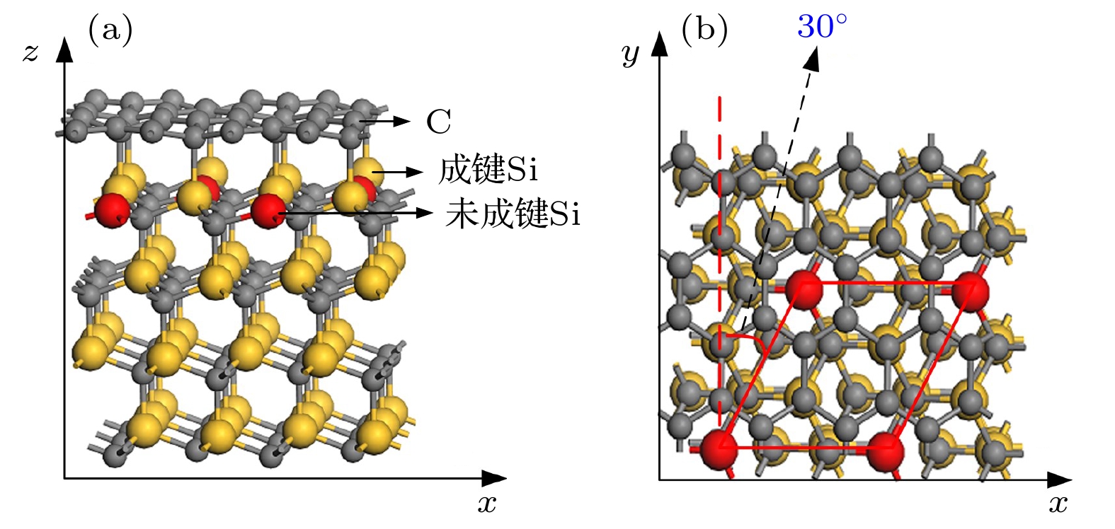
图 1 单层石墨烯/SiC (0001)的接触界面 (a) 侧视图; (b) 俯视图
Fig. 1. Side view (a) and top view (b) of single-layer graphene on SiC(0001) surface.
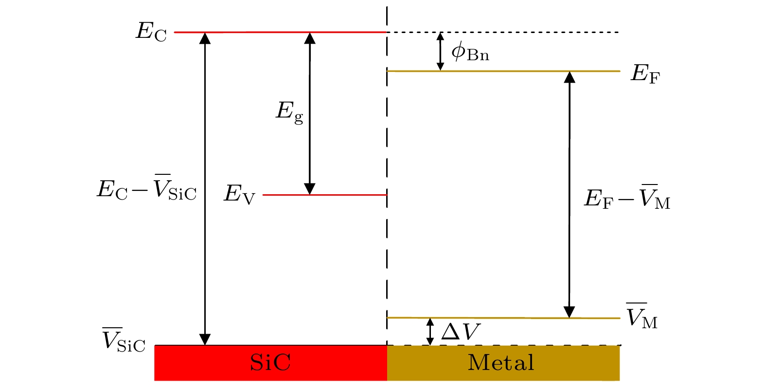
图 2 金属/SiC接触界面SBH与平均静电势关系的能带结构
Fig. 2. Schematic band diagram shows the relationship between SBH and planar-averaged local potentials for metal/SiC contact.
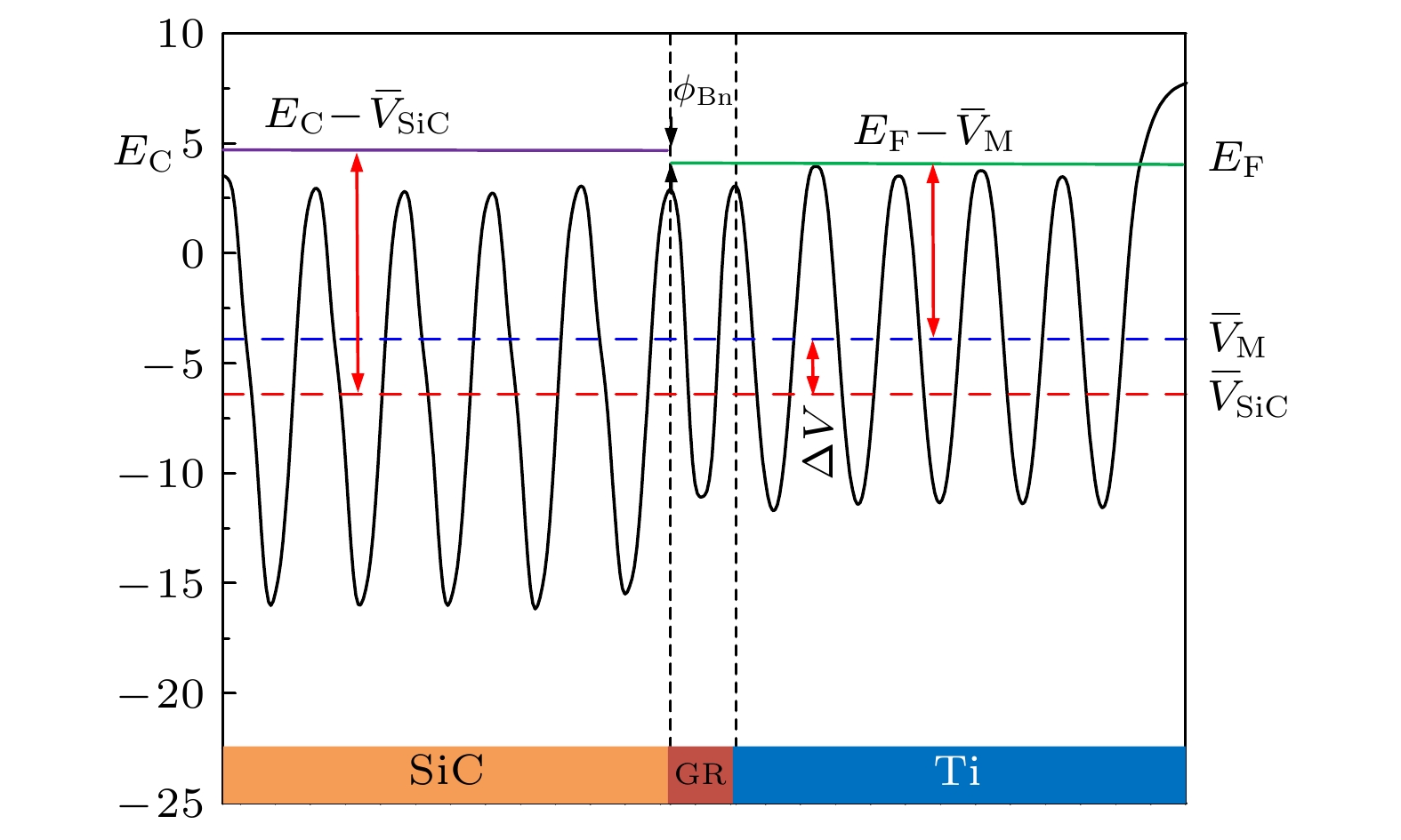
图 3 Ti/1GR/SiC沿z轴的平均静电势
Fig. 3. The planar-averaged local potential for Ti/1GR/SiC along the z-axis.

图 4 不同层数石墨烯过渡层对金属/SiC接触SBH的影响
Fig. 4. The effects of graphene intercalation on the SBH of metal/SiC contacts.
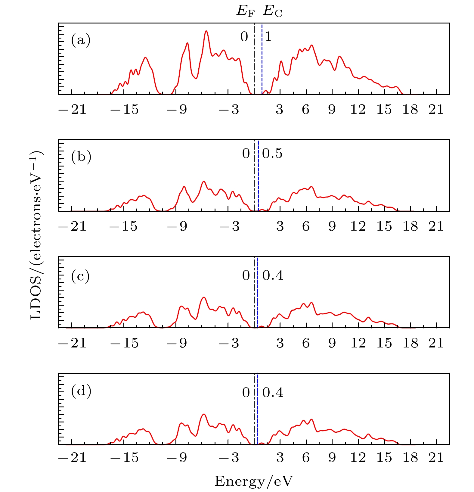
图 5 Cu(111)/SiC体系在SiC区域的局域态密度图 (a) Cu/SiC; (b) Cu/1GR/SiC; (c) Cu/2GR/SiC; (d) Cu/3GR/SiC
Fig. 5. Local density of states of SiC region for (a) Cu/SiC, (b) Cu/1GR/SiC, (c) Cu/2GR /SiC, and (d) Cu/3GR/SiC systems.
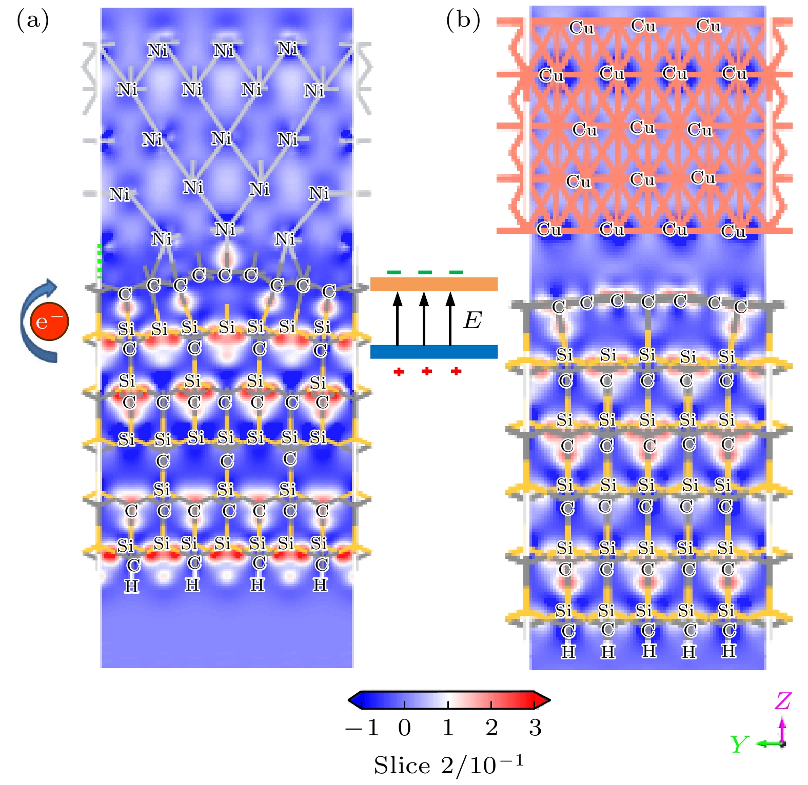
图 6 (a) Ni/1GR/4H-SiC(0001) 和 (b) Cu/1GR/4H-SiC(0001)的差分电荷密度图, 蓝色区域代表失去电子, 红色区域代表得到电子
Fig. 6. The difference of charge density for (a) the Ni/1GR/4H-SiC (0001) and (b) the Cu/1GR/4H-SiC (0001). The blue regions represent losing electrons. The red regions represent gaining electrons.
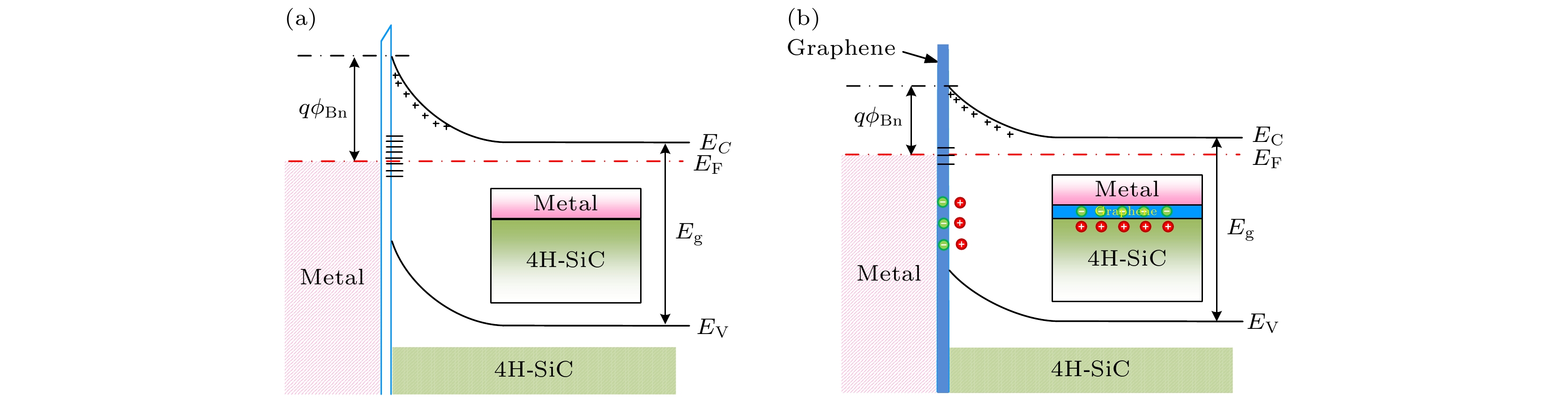
图 7 (a) 金属/4H-SiC和 (b) 金属/GR/4H-SiC接触界面能带图
Fig. 7. Schematic band diagrams of (a) metal/4H-SiC and (b) metal/GR/4H-SiC.

图 8 (a) Ti/4H-SiC, (b) Ti/1GR/4H-SiC, (c) Ti/2GR/4H-SiC, (d) Ti/3GR/4H-SiC 以及 (e) Pt/1GR/4H-SiC SiC顶层碳硅层的局域态密度图
Fig. 8. Local density of states of the first carbon silicon layer for (a) Ti/4H-SiC, (b) Ti/1GR/ 4H-SiC, (c) Ti/2GR/4H-SiC, (d) Ti/3GR/4H-SiC and (e) Pt/1GR/4H-SiC.
表 1 Cu不同切面与4H-SiC(0001)接触体系的
$ {E_{{\text{M/SiC}}}} $ ,$ {E_{\text{M}}} $ ,$ {E_{{\text{SiC}}}} $ 和$ {W_{{\text{ad}}}} $ Table 1.
$ {E_{{\text{M/SiC}}}} $ ,$ {E_{\text{M}}} $ ,$ {E_{{\text{SiC}}}} $ and$ {W_{{\text{ad}}}} $ values for the different Cu planes contact to 4H-SiC(0001).界面体系 $ {E_{{\text{M/SiC}}}} $/eV $ {E_{\text{M}}} $/eV $ {E_{{\text{SiC}}}} $/eV $ {W_{{\text{ad}}}} $/$(\rm J {\cdot} c{m^{ - 2} })$ Cu(111)/4H-SiC(0001) –154329.42 –134459.95 –19851.12 0.0562 Cu(110)/4H-SiC(0001) –164264.27 –134455.87 –29790.06 0.0279 Cu(001)/4H-SiC(0001) –154340.26 –134456.34 –19865.27 0.0515  下载: 导出CSV
表 2 晶格失配后各金属超胞的Wm与理论值和文献[26]中实验值对比
Table 2. The calculated Wm values of the metal supercells after lattice mismatching, compared with the theoretical and the experimental values in reference [26].
Metal Wm/eV 理论值/eV 实验值[26]/eV Ag 4.52 4.19 4.26 Ti 4.43 4.38 4.33 Cu 4.68 4.51 4.65 Pd 5.16 4.89 5.12 Ni 5.12 4.92 5.15 Pt 5.76 5.31 5.65
下载: 导出CSV
表 3 平均静电势与局域态密度计算方法计算的各接触体系
${\phi _{{\text{Bn}}}}$ 值 (单位: eV)Table 3.
${\phi _{{\text{Bn}}}}$ values for the contacts obtained from planar averaged electrostatic potential and local density of states calculation methods (in eV).计算方法 GR layers Ag Ti Cu Pd Ni Pt 平均静电势法 0 1.2 1.5 1.2 1.5 1.1 1.6 1 0.25 0.5 0.7 0.6 0.25 1.4 2 0.1 –0.1 0.6 0.5 –0.45 0.8 3 0.1 –0.1 0.6 0.5 –0.45 0.8 局域态密度法 0 1 1.2 1 1.3 1 1.3 1 0.2 0.3 0.5 0.4 0.2 1 2 0.1 –0.15 0.4 0.3 –0.5 0.9 3 0.1 –0.15 0.4 0.3 –0.5 0.9
下载: 导出CSV
-
[1] Tian R, Ma C, Wu J, Guo Z, Yang X, Fan Z 2021 J. Semicond. 42 061801
Google Scholar
[2] Wang Z T, Liu W, Wang C Q 2016 J. Electron. Mater. 45 267
Google Scholar
[3] Huang L Q, Xia M L, Gu X G 2020 J. Cryst. Growth. 531 125353
Google Scholar
[4] Kuchuk A V, Borowicz P, Wzorek M, Borysiewicz M, Ratajczak R, Golaszewska K, Kaminska E, Kladko V, Piotrowska A 2016 Adv. Cond. Matter. Phys. 2016 9273702
Google Scholar
[5] Al-Ahmadi N A 2020 Mater. Res. Express 7 032001
Google Scholar
[6] Nikitina I P, Vassilevski K V, Wright N G, Horsfall A B, O’Neill A G, Johnson C M 2005 J. Appl. Phys. 97 083709
Google Scholar
[7] Liu F, Hsia B, Carraro C, Pisano A P, Maboudian R 2010 Appl. Phys. Lett. 97 262107
Google Scholar
[8] Seyller T, Emtsev K V, Speck F, Gao K Y, Ley L 2006 Appl. Phys. Lett. 88 242103
Google Scholar
[9] Lundberg N, Östling M 1993 Appl. Phys. Lett. 63 3069
Google Scholar
[10] Reshanov S A, Emtsev K V, Speck F, Gao K Y, Seyller T K, Pensl G, Ley L 2008 Phys. Status Solidi B 245 1369
Google Scholar
[11] 黄玲琴, 朱靖, 马跃, 梁庭, 雷程, 李永伟, 谷晓钢 2021 物理学报 70 207302
Google Scholar
Huang L Q, Zhu J, Ma Y, Liang T, Lei C, Li Y W, Gu X G 2021 Acta Phys. Sin. 70 207302
Google Scholar
[12] Huang L Q, Xia M L, Ma Y, Gu X G 2020 J. Appl. Phys. 127 25301
Google Scholar
[13] Nagashio K, Nishimura T, Kita K, Toriumi A 2009 International Electron Devices Meeting (IEDM) Baltimore, MD December 7–9, 2009 p527
[14] Røst H I, Chellappan R K, Strand F S, Grubišić-Čabo A, Reed B P, Prieto M J, Tǎnase L C, Caldas L D S, Wongpinij T, Euaruksakul C, Schmidt T, Tadich A, Cowie B C C, Li Z, Cooil S P, Wells J W 2021 J. Phys. Chem. C 125 4243
Google Scholar
[15] Yoon H H, Song W, Jung S, Kim J, Mo K, Choi G, Jeong H Y, Lee J H, Park K 2019 ACS Appl. Mater. Inter. 11 47182
Google Scholar
[16] Wu Y, Ji L, Lin Z, Hong M, Wang S, Zhang Y 2019 Curr. Appl. Phys. 19 521
Google Scholar
[17] Jia Y, Sun X, Shi Z, Jiang K, Wu T, Liang H, Cui X, Lü W, Li D 2021 Diamond. Relat. Mater. 115 108355
Google Scholar
[18] Segall M D, Lindan P J, Probert M A, Pickard C J, Hasnip P J, Clark S J, Payne M C 2002 J. Phys. Condens. Matter 14 2717
Google Scholar
[19] Perdew J P, Kieron B, Matthias E 1996 Phys. Rev. Lett. 77 3865
Google Scholar
[20] Ceperley D M, Berni J A 1980 Phys. Rev. Lett. 45 566
Google Scholar
[21] Grimme S, Antony J, Ehrlich S, Krieg H 2010 J. Chem. Phys. 132 154104
Google Scholar
[22] 王奇, 唐法威, 侯超, 吕皓, 宋晓艳 2019 物理学报 68 077101
Google Scholar
Wang Q, Tang F W, Hou C, Lv H, Song X Y 2019 Acta Phys. Sin. 68 077101
Google Scholar
[23] Mattausch A, Pankratov O 2007 Phys. Rev. Lett. 99 076802
Google Scholar
[24] Xu B, Zhu C, He X, Zang Y, Lin S, Li L, Feng S, Lei Q 2018 Adv. Condens. Matter Phys. 2018 8010351
[25] Li L, Jin W, Yang H, Gao K, Guo P, Pang X, Volinsky A A. 2018 Microelectron. Reliab. 83 119
Google Scholar
[26] Michaelson H B 1977 J. Appl. Phys. 48 4729
Google Scholar
[27] Oh Y J, Lee A T, Noh H K, Chang K J 2013 Phys. Rev. B 87 075325
Google Scholar
[28] Kohyama M, Hoekstra J 2000 Phys. Rev. B 61 2672
Google Scholar
[29] Tanaka S, Tamura T, Okazaki K, Ishibashi S, Kohyama M 2006 Mater. Trans. 47 2690
Google Scholar
[30] Profeta G, Blasetti A, Picozzi S, Continenza A, Freeman A. J 2001 Phys. Rev. B 64 235312
Google Scholar
[31] Kozlov S M, Vines F, Görling A 2012 J. Phys. Chem. C 116 7360
Google Scholar
[32] Cicek A, Bülent U L U Ğ 2021 Balkan J. Electr. Comput. Eng. 9 171
[33] 王菁, 李美成 2000 半导体光电 21 261
Google Scholar
Wang J, Li M C 2000 Semicond. Opt. 21 261
Google Scholar
[34] Chen Y, Xu X, Liu P 2019 J. Phys. Chem. C 124 1362
[35] Li J B, Wang X H, Wang W J 2020 J. Infrared Millimeter Waves 39 401
[36] Song S M, Park J K, Sul O J, Cho B J 2012 Nano Lett. 12 3887
Google Scholar
[37] Heine V 1965 Phys. Rev. 138 A1689
Google Scholar
[38] Sajjad M, Yang X, Altermatt P, Singh N, Schwingenschlögl U, Wolf D S 2019 Appl. Phys. Lett. 114 071601
Google Scholar

 下载:
下载:


计量
- 文章访问数: 11944
- PDF下载量: 284
- 被引次数: 0
