


-
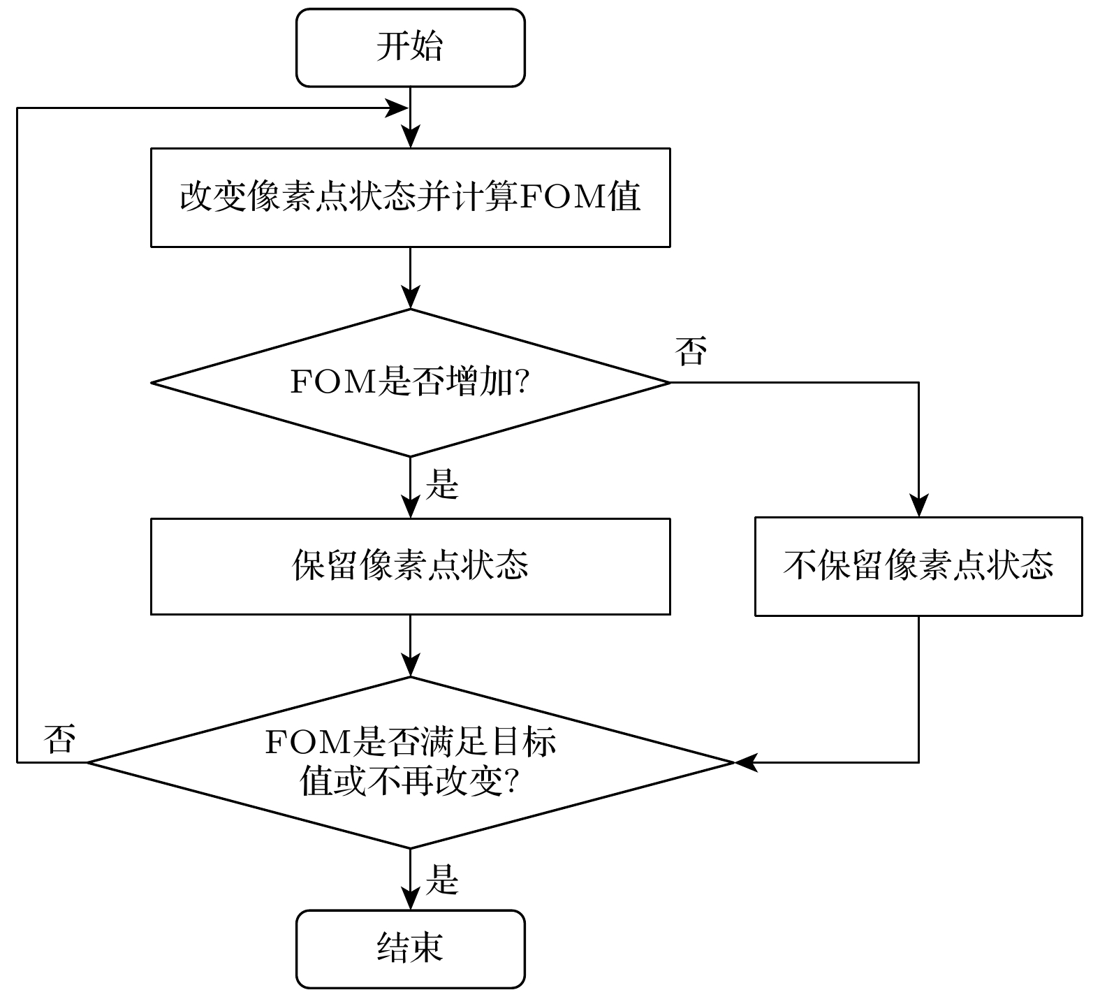
多模干涉耦合器结构的功率分束器拥有大带宽、较好制造鲁棒性等优势, 长期以来受到人们的关注. 本文提出的是一种基于相变材料In2Se3的超紧凑可调控功率分束器, 尺寸仅有2.4 μm×3.6 μm, 采用1×2的多模干涉耦合器结构, 在不改变其他结构参数的情况下, 采用直接二进制搜索算法对器件进行优化, 仅通过In2Se3的α态与β态的可逆相变, 利用两种晶态之间的高折射率对比度实现了不同的功率分束比. 与其他可调控的功率分束器相比, 本文设计的这种功率分束器结构紧凑、调控简单, 并且具有较好的鲁棒性. 利用该器件在1540—1560 nm的波长范围内实现了1∶1, 1∶1.5, 1∶2三种分束比, 插入损耗分别小于0.27, 0.13和0.17 dB. 证明了这种基于相变材料In2Se3的超紧凑可调控功率分束器在光子集成电路上应用的可能性.Power splitter with multi-mode interference coupler structure has many advantages, such as large bandwidth and better manufacturing robustness, and has received much attention for a long time. Conventional power beam splitters usually use algorithms or numerical simulation to achieve a single beam splitting ratio; if the circuit has the requirement for power, the structural parameters of the device need changing and recalculating. In order to improve the utilization rate of power splitter in photonic integrated circuit and meet various demands for different optical paths, an ultra-compact tunable power splitter based on phase change material In2Se3 with a 1×2 multimode interference coupler structure is proposed in this paper. The device consists of an input waveguide, a coupling region, and two output waveguides with a coupling region of only 2.4 μm× 3.6 μm in size, which contains several circular holes of the same size and is filled with SiO2. The number and location of circular holes in the coupling region are optimized by direct binary search algorithm, making the device achieve different power splitting ratios by using only the high refractive index contrast variation between the two crystalline states (α and β) of In2Se3 without changing any other structural parameter. In a wavelength range of 1540–1560 nm, three splitting ratios of 1∶1, 1∶1.5 and 1∶2 are achieved by this device, and the insertion losses of these three beam splitting ratios are less than 0.27, 0.13 and 0.17 dB, respectively. In addition, the robustness and balance of the device are analyzed and discussed, and compared with those of the power splitter of the same size designed by SOI platform and several power beam splitters reported in recent years, demonstrating the compact structure and simple regulation of this power splitter based on the phase change material In2Se3, its good robustness, and its possibility of application on photonic integrated circuits.
-
Keywords:
- power beam splitter /
- phase change materials /
- reverse design /
- integrated optics
[1] Zhu J B, Chao Q, Huang H Y, Zhao Y X, Li Y, Tao L, She X J, Liao H, Huang R, Zhu Z J, Liu X, Sheng Z, Gan F W 2021 Appl. Opt. 60 413
 Google Scholar
[2] Zhang C P, Zhang M, Xie Y W, Shi Y C, Kumar R, Panepucci R R, Dai D X 2020 Photonics Res. 8 1171
Google Scholar
[3] Fang Z R, Chen R, Zhang J Y, Xu P P, Majumdar A 2022 Conference on Lasers and Electro-Optics San Jose, California United States, May 15–20, 2022 pp1,2
[4] Wang N N, Li T T, Sun B S, Wang Z, Zhou L J, Gu T Y 2021 Opt. Lett. 46 4088
Google Scholar
[5] Song C M, Gao Y X, Wang G X, Chen Y M, Xu P P, Gu C J, Shi Y C, Shen X 2022 Opt. Express 30 30430
Google Scholar
[6] Tao X, Gu Y 2013 Nano Lett. 13 3501
Google Scholar
[7] Xu K, Jiang W, Gao X S, Zhao Z J, Low T, Zhu W J 2020 Nanoscale 12 23488
Google Scholar
[8] Lee H, Kang D H, Tran L 2005 Mater. Sci. Eng. , B 119 196
Google Scholar
[9] Botcha V D, Hong Y H, Huang Z H, Li Z W, Liu Q, Wu J, Lu Y M, Liu X K 2019 J. Alloys Compd. 773 698
Google Scholar
[10] Lee H, Kang D H 2005 Jpn. J. Appl. Phys. 44 4759
Google Scholar
[11] Huang Y T, Chen N K, Li Z Z, Wang X P, Sun H B, Zhang S B, Li X B 2022 InfoMat 4 e12341
Google Scholar
[12] Li T T, Wang Y, Li W, Mao D, Benmore C J, Evangelista I, Xing H D, Li Q, Wang F F, Sivaraman G, Janotti A, Law S, Gu T Y 2022 Adv. Mater. 34 e2108261
Google Scholar
[13] Taghinejad H, Abdollahramezani S, Eftekhar A A, Fan T R, Hosseinnia A H, Hemmatyar O, Dorche A E, Gallmon A, Adibi A 2021 Opt. Express 29 20449
Google Scholar
[14] Zheng J J, Khanolkar A, Xu P P, Colburn S, Deshmukh S, Myers J, Frantz J, Pop E, Hendrickson J, Doylend J, Boechler N, Majumdar A 2018 Opt. Mater. Express 8 1551
Google Scholar
[15] Yuan H, Wu J G, Zhang J P, Pu X, Zhang Z F, Yu Y, Yang J B 2022 Nanomaterials 12 669
Google Scholar
[16] Ríos C, Zhang Y F, Shalaginov M Y, Deckoff-Jones S, Wang H Z, An S S, Zhang H L, Kang M, Richardson K A, Roberts C, Chou J B, Liberman V, Vitale S A, Kong J, Gu T, Hu J J 2021 Adv. Photonics Res. 2 2000034
Google Scholar
[17] Liu T Y, Xu Y, Liu S Y, Sun X Q, Zhang D M 2022 Opt. Mater. Express 12 2584
Google Scholar
[18] Su Y X, Liu D M, Zhang M M 2022 Opt. Express 30 40379
Google Scholar
[19] Wei J, Rajesh M, Berardi S R 2021 Opt. Mater. Express 11 3007
Google Scholar
[20] Li T T, Wang Y, Xing H D, Li Q, Wang F F, Soman A, Law S, Gu T Y 2021 Conference on Lasers and Electro-optics Electr Network, May 9–14, 2021 pSM4B.5
[21] Behera B, Sutar B C, Pradhan N R 2021 Emergent Mater. 4 847
Google Scholar
[22] Li J Y, Li H D, Niu X B, Wang Z M 2021 ACS Nano 15 18683
Google Scholar
[23] Forouzmand A, Mosallaei H 2018 Opt. Express 26 17948
Google Scholar
[24] Xu K, Liu L, Wen X, Sun W Z, Zhang N, Yi N B, Sun S, Xiao S M, Song Q H 2017 Opt. Lett. 42 855
Google Scholar
-
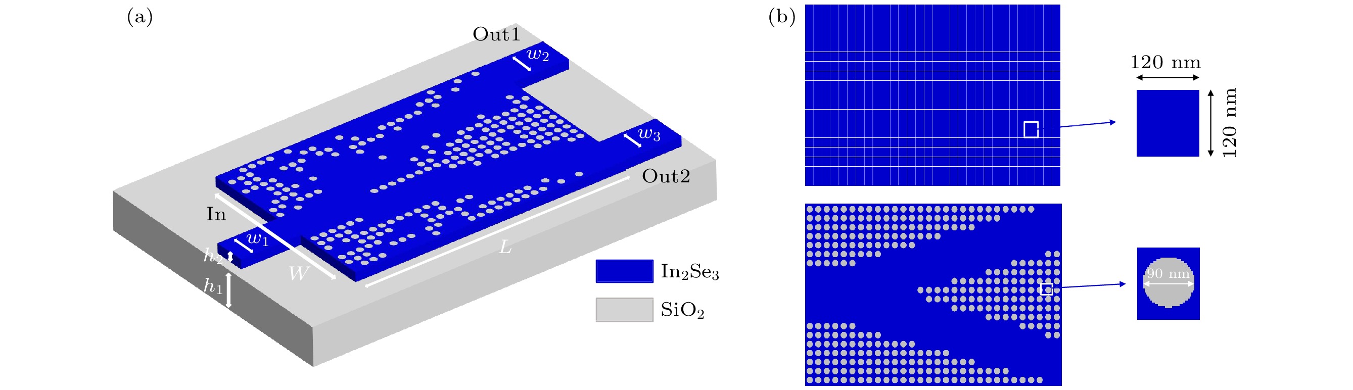
图 1 器件整体结构 (a) 优化后得到的结果和器件的参数, 其中Out1与Out2为器件的两个输出端口; (b) 初始化时划分好的像素点网格和圆孔的初始位置
Fig. 1. Overall device structure: (a) Optimized results and device parameters, where Out1 and Out2 are the two output ports of the device; (b) the initial position of the divided pixel grid and the air hole during initialization.

图 3 通过模拟仿真得到的3种分束比下的结果 (a) In2Se3在α态时实现的1∶1分束比; (b) 1∶1分束比下两个端口的透过率; (c) In2Se3在中间混合态时实现的1∶1.5分束比; (d) 1∶1.5分束比下两个端口的透过率; (e) In2Se3在β态时实现的1∶2分束比; (f) 1∶2分束比下两个端口的透过率
Fig. 3. Results obtained by simulation for three beam splitting ratios: (a) 1:1 beam splitting ratio achieved for In2Se3 in the α state; (b) transmittance of two ports at 1∶1 beam splitting ratio; (c) 1∶1.5 beam splitting ratio achieved by In2Se3 in the intermediate mixed state; (d) transmittance of both ports at 1∶1.5 beam splitting ratio. (e) 1∶2 beam splitting ratio achieved by In2Se3 in the beta state; (f) transmittance of two ports at 1∶2 beam splitting ratio.

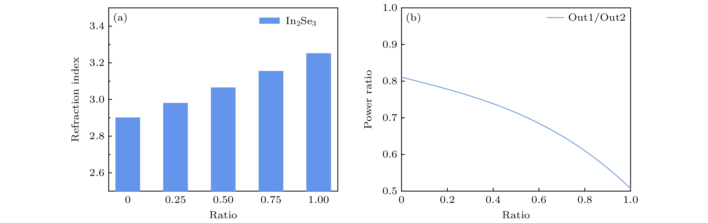
图 5 (a) In2Se3的α态与β态在混合态中占比对折射率的影响; (b) In2Se3在相变过程中实现的分束比变化
Fig. 5. (a) Influence of the proportion of α and β states of In2Se3 in the mixed state on the refractive index; (b) variation of the upper and lower port splitting ratio in In2Se3 phase transition.

图 6 SOI平台与In2Se3设计的功率分束器在实现相同分束比时的打孔情况 (a) SOI平台实现1∶1, 1∶1.5, 1∶2分束比的功率分束器; (b) In2Se3材料实现 1∶1, 1∶1.5, 1∶2分束比的功率分束器; (c) SOI平台与In2Se3实现各个分束比时的IL对比
Fig. 6. Perforation of SOI platform and In2Se3 designed power beam splitters in achieving the same beam splitting ratio: (a) SOI platform realizing power beam splitters with 1∶1, 1∶1.5, and 1∶2 beam splitting ratios; (b) In2Se3 material realizing power beam splitters with 1∶1, 1∶1.5, and 1∶2 beam splitting ratios; (c) IL comparison between SOI platform and In2Se3 when realizing each beam splitting ratio.

图 7 圆孔直径对器件的影响 (a) In2Se3在α态时圆孔直径误差在5 nm范围内的IL; (b) In2Se3在中间混合态时圆孔直径误差在5 nm范围内的IL; (c) In2Se3在β态时圆孔直径误差在5 nm范围内的IL; (d) In2Se3在α态时圆孔直径误差在5 nm范围内的平衡误差; (e) In2Se3在中间混合态时圆孔直径误差在5 nm范围内的平衡误差; (f) In2Se3在β态时圆孔直径误差在5 nm范围内的平衡误差
Fig. 7. Effect of air circular hole diameter on the device: (a) IL of In2Se3 in α state with circular hole diameter error in the range of 5 nm; (b) IL of In2Se3 in intermediate mixed state with circular hole diameter error in the range of 5 nm; (c) IL of In2Se3 in β state with circular hole diameter error in the range of 5 nm; (d) the equilibrium error of In2Se3 in α state with circular hole diameter error in the range of 5 nm; (e) the equilibrium error of In2Se3 in the intermediate mixed state with a circular hole diameter error in the range of 5 nm; (f) the equilibrium error of In2Se3 in the β-state with a circular hole diameter error in the range of 5 nm.
表 1 几种相变材料的光学性能比较(A, 非晶态; C, 晶态; k, 消光系数)
Table 1. Comparison of optical properties of several phase change materials ( A, amorphous; C, crystalline; k, extinction coefficients).
Phase change
temperature/°CΔn (1550 nm) Reversibility k (1550 nm) Ge2Sb2Te5 (GST) A → C, >600[13]
C → A, 200[14]2.85[15] yes kA = 0.12,
kC = 1.49[15]Ge2Sb2Se4Te1 (GSST) A → C, ~270
C → A, >600[16]1.625[17] yes kA ~ 0,
kC = 0.42[17]Sb2Se3 A → C, ~200
C → A, ~600[18]1.22[18] yes kA ~ 0,
kC ~ 0[19]In2Se3 α → β, 200
β → β', 200
β' → α, 60[12]~0.35[12] yes kα = 0,
kβ = 0[12] 下载: 导出CSV
表 2 目前报道的几种功率分束器与本文设计的功率分束器的比较
Table 2. Comparison of several power splitters reported at present with the power splitter designed in this paper.
文献[24](2017) 文献[1](2021) 文献[15](2022) This work Dimension 3.6 µm×3.6 µm Ltaper = 80 µm 2.4 µm×2.4 µm 3.6 µm×2.4 µm Material Si Si3N4 GSST In2Se3 Type MMI adiabatic tapers MMI MMI Structure 


Bandwidth/nm 1530—1560 1500—1600 1530—1560 1540—1560 Adjustable no no yes yes Excess loss/dB 0.97 0.02 <0.5 (1∶1)
<0.83 (1.5∶1)
<1.2 (2∶1)
<1.18 (2.5∶1)<0.27 (1∶1)
<0.13 (1∶1.5)
<0.17 (1∶2)Method FSM Numerical simulations DBS DBS
下载: 导出CSV
-
[1] Zhu J B, Chao Q, Huang H Y, Zhao Y X, Li Y, Tao L, She X J, Liao H, Huang R, Zhu Z J, Liu X, Sheng Z, Gan F W 2021 Appl. Opt. 60 413
Google Scholar
[2] Zhang C P, Zhang M, Xie Y W, Shi Y C, Kumar R, Panepucci R R, Dai D X 2020 Photonics Res. 8 1171
Google Scholar
[3] Fang Z R, Chen R, Zhang J Y, Xu P P, Majumdar A 2022 Conference on Lasers and Electro-Optics San Jose, California United States, May 15–20, 2022 pp1,2
[4] Wang N N, Li T T, Sun B S, Wang Z, Zhou L J, Gu T Y 2021 Opt. Lett. 46 4088
Google Scholar
[5] Song C M, Gao Y X, Wang G X, Chen Y M, Xu P P, Gu C J, Shi Y C, Shen X 2022 Opt. Express 30 30430
Google Scholar
[6] Tao X, Gu Y 2013 Nano Lett. 13 3501
Google Scholar
[7] Xu K, Jiang W, Gao X S, Zhao Z J, Low T, Zhu W J 2020 Nanoscale 12 23488
Google Scholar
[8] Lee H, Kang D H, Tran L 2005 Mater. Sci. Eng. , B 119 196
Google Scholar
[9] Botcha V D, Hong Y H, Huang Z H, Li Z W, Liu Q, Wu J, Lu Y M, Liu X K 2019 J. Alloys Compd. 773 698
Google Scholar
[10] Lee H, Kang D H 2005 Jpn. J. Appl. Phys. 44 4759
Google Scholar
[11] Huang Y T, Chen N K, Li Z Z, Wang X P, Sun H B, Zhang S B, Li X B 2022 InfoMat 4 e12341
Google Scholar
[12] Li T T, Wang Y, Li W, Mao D, Benmore C J, Evangelista I, Xing H D, Li Q, Wang F F, Sivaraman G, Janotti A, Law S, Gu T Y 2022 Adv. Mater. 34 e2108261
Google Scholar
[13] Taghinejad H, Abdollahramezani S, Eftekhar A A, Fan T R, Hosseinnia A H, Hemmatyar O, Dorche A E, Gallmon A, Adibi A 2021 Opt. Express 29 20449
Google Scholar
[14] Zheng J J, Khanolkar A, Xu P P, Colburn S, Deshmukh S, Myers J, Frantz J, Pop E, Hendrickson J, Doylend J, Boechler N, Majumdar A 2018 Opt. Mater. Express 8 1551
Google Scholar
[15] Yuan H, Wu J G, Zhang J P, Pu X, Zhang Z F, Yu Y, Yang J B 2022 Nanomaterials 12 669
Google Scholar
[16] Ríos C, Zhang Y F, Shalaginov M Y, Deckoff-Jones S, Wang H Z, An S S, Zhang H L, Kang M, Richardson K A, Roberts C, Chou J B, Liberman V, Vitale S A, Kong J, Gu T, Hu J J 2021 Adv. Photonics Res. 2 2000034
Google Scholar
[17] Liu T Y, Xu Y, Liu S Y, Sun X Q, Zhang D M 2022 Opt. Mater. Express 12 2584
Google Scholar
[18] Su Y X, Liu D M, Zhang M M 2022 Opt. Express 30 40379
Google Scholar
[19] Wei J, Rajesh M, Berardi S R 2021 Opt. Mater. Express 11 3007
Google Scholar
[20] Li T T, Wang Y, Xing H D, Li Q, Wang F F, Soman A, Law S, Gu T Y 2021 Conference on Lasers and Electro-optics Electr Network, May 9–14, 2021 pSM4B.5
[21] Behera B, Sutar B C, Pradhan N R 2021 Emergent Mater. 4 847
Google Scholar
[22] Li J Y, Li H D, Niu X B, Wang Z M 2021 ACS Nano 15 18683
Google Scholar
[23] Forouzmand A, Mosallaei H 2018 Opt. Express 26 17948
Google Scholar
[24] Xu K, Liu L, Wen X, Sun W Z, Zhang N, Yi N B, Sun S, Xiao S M, Song Q H 2017 Opt. Lett. 42 855
Google Scholar

 下载:
下载:
计量
- 文章访问数: 5126
- PDF下载量: 127
- 被引次数: 0
