


-
随着半导体芯片特征尺寸的持续减小, 低介电常数的多孔材料在微电子领域得到广泛应用. 然而, 多孔材料在等离子体刻蚀工艺中面对严峻的挑战. 等离子体中的活性自由基很容易在多孔材料内部扩散, 并与材料发生不可逆的化学反应, 在材料内部造成大面积损伤. 本文介绍了业内比较前沿的低温刻蚀技术, 通过降低基片台的温度, 使得刻蚀产物或者刻蚀前驱气体在多孔材料内部凝结成液态或者固态, 进而在等离子体刻蚀过程中, 阻止活性自由基在材料内部的扩散, 保护多孔材料免受损伤. 刻蚀完毕后, 再通过升高基片台的温度, 使凝结物挥发, 得到完整无损的刻蚀结构. 这一刻蚀技术只需要控制基片台的温度, 无需增加工艺的复杂度以及调整等离子体状态, 在半导体工艺中具有较好的应用前景.With the shrinkage of chip feature sizes, porous materials are widely used in microelectronics. However, they are facing severe challenges in plasma etching, as the reactive radicals can diffuse into the interior of material and damage the material, which is called plasma induced damage. In this paper, we review two kinds of etching processes based on low chuck temperature, i.e. cryogenic etching. By lowering the chuck temperature, either the etching by-products or the precursor gas can condense in the porous material, and thus preventing the radicals from diffusing and protect the material from being damaged by plasma. The technology of cryogenic filling inside the porous material is simple but effective, which allows it to have a good application prospect.
-
Keywords:
- low temperature plasma /
- porous material /
- plasma induced damage /
- cryogenic etching /
- pore filling
[1] Sicard E, Boyer A 2019 EMC Compo Haining, China, October 21–23, 2019 ffhal-02403882
[2] [3] 王婷婷, 叶超, 宁兆元, 程珊华 2005 物理学报 54 892
 Google Scholar
Wang T T, Ye C, Ning Z Y, Cheng S H 2005 Acta Phys. Sin. 54 892
Google Scholar
[4] Zhang L, Marneffe J F, Heyne M, Naumov S, Sun Y T, et al. 2015 ECS J. Solid State Sci. Technol. 4 N3098
Google Scholar
[5] Baklanov M, Marneffe J F, Shamiryan D, Urbanowicz A, Shi H, Rakhimova T, Huang H, Ho P 2013 J. Appl. Phys. 113 041101
Google Scholar
[6] Lionti K, Volksen W, Magbitang T, Darnon M, Dubois G 2015 ECS J. Solid State Sci. Technol. 4 N3071
Google Scholar
[7] Frot T, Volksen W, Purushothaman S, Bruce R, Dubois G 2011 Adv. Mater. 23 2828
Google Scholar
[8] Frot T, Volksen W, Purushothaman S, Bruce R L, Magbitang T, Miller D C, Deline V R, Dubois G 2012 Adv. Funct. Mater. 22 3043
Google Scholar
[9] Tachi S, Tsujimoto K, Okudaira S 1988 Appl. Phys. Lett. 52 616
Google Scholar
[10] Tachi S, Tsujimoto K, Arai S, Kure T 1991 J. Vac. Sci. Technol., A 9 796
Google Scholar
[11] Tsujimoto K, Okudaira S, Tachi S 1991 Jpn. J. Appl. Phys. 30 3319
Google Scholar
[12] Zhang L, Ljazouli R, Lefaucheux P, Tillocher T, Dussart R, Mankelevich Y A, de Marneffe J F, de Gendt S, Baklanov M R 2013 ECS Solid State Lett. 2 N5
Google Scholar
[13] Zhang L, Ljazouli R, Lefaucheux P, Tillocher T, Dussart R, Mankelevich Y A, de Marneffe J F, de Gendt S, Baklanov M R 2013 ECS J. Solid State Sci. Technol. 2 N131
Google Scholar
[14] Zhang L, de Marneffe J F, Leroy F, Lefaucheux P, Tillocher T, Dussart R, Maekawa K, Yatsuda K, Dussarrat C, Goodyear A, Cooke M, De Gendt S, Baklanov M R 2016 J. Phys. D: Appl. Phys. 49 175203
Google Scholar
[15] Dussart R, Tillocher T, Lefaucheux P, Boufnichel M 2014 J. Phys. D: Appl. Phys. 47 123001
Google Scholar
[16] Chanson R, Zhang L, Naumov S, Mankelevich Yu A, Tillocher T, Lefaucheux P, Dussart R, De Gendt S, De Marneffe J F 2018 Sci. Rep. 8 1886
Google Scholar
[17] Chanson R, Tahara S, Vanstreels K, de Marneffe J F 2018 Plasma Research Express 1 015006
Google Scholar
[18] Chanson R, Dussart R, Tillocher T, Lefaucheux P, Dussarrat C, De Marneffe J F 2019 Front. Chem. Sci. Eng. 13 511
Google Scholar
[19] Rezvanov A, Miakonkikh A, Vishnevskiy A, Rudenko K, Baklanov M 2017 J. Vac. Sci. Technol. B 35 021204
Google Scholar
[20] Kushner M 2009 J. Phys. D: Appl. Phys. 42 194013
Google Scholar
[21] Sankaran A, Kushner M J 2004 Vac. Sci. Technol., A 22 1242
[22] 胡艳婷, 张钰如, 宋远红, 王友年 2018 物理学报 67 225203
Google Scholar
Hu Y T, Zhang Y R, Song Y H, Wang Y N 2018 Acta Phys. Sin. 67 225203
Google Scholar
[23] 蒋相占, 刘永新, 毕振华, 陆文琪, 王友年 2012 物理学报 61 015204
Google Scholar
Jiang X Z, Liu Y X, Bi Z H, Lu W Q, Wang Y N 2012 Acta Phys. Sin. 61 015204
Google Scholar
[24] Zhang Q Z, Tink S, De Marneffe J F, Zhang L P, Bogaerts A 2017 Appl. Phys. Lett. 111 173104
Google Scholar
[25] Zhang Q Z, Jiang W, Hou L J, Wang Y N 2011 J. Appl. Phys. 109 013308
Google Scholar
-
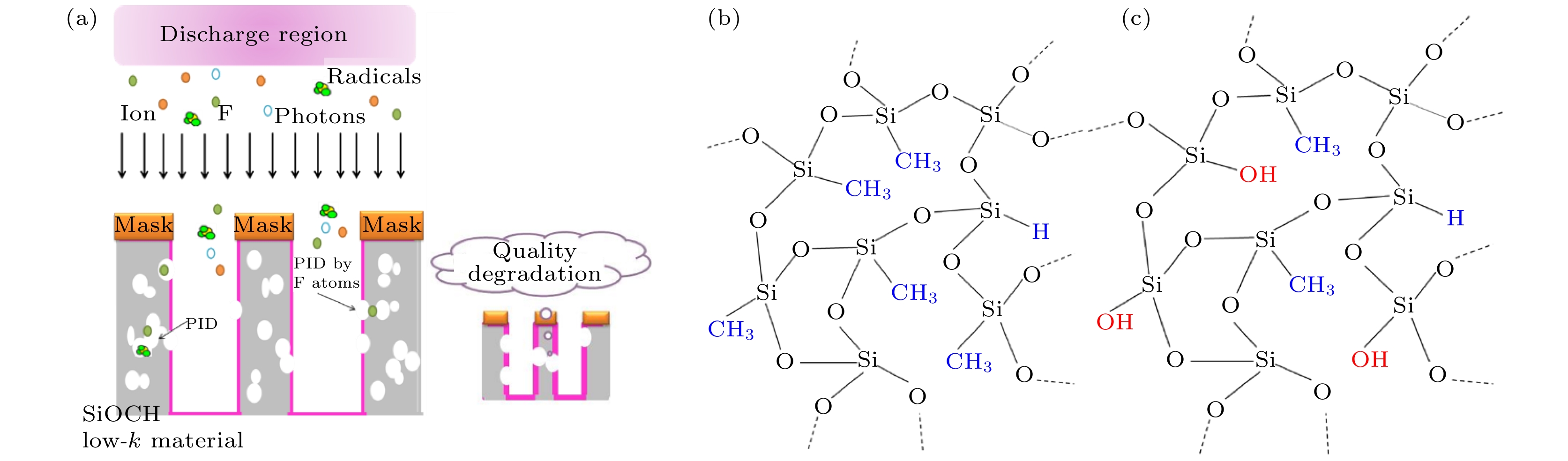

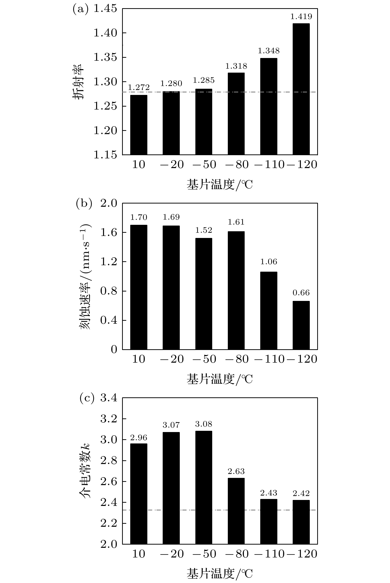
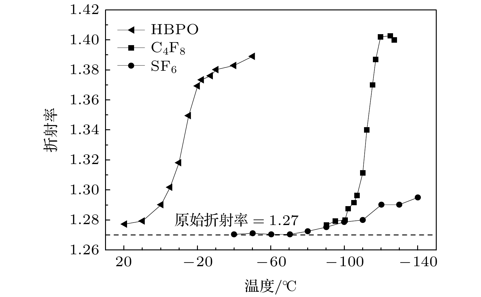
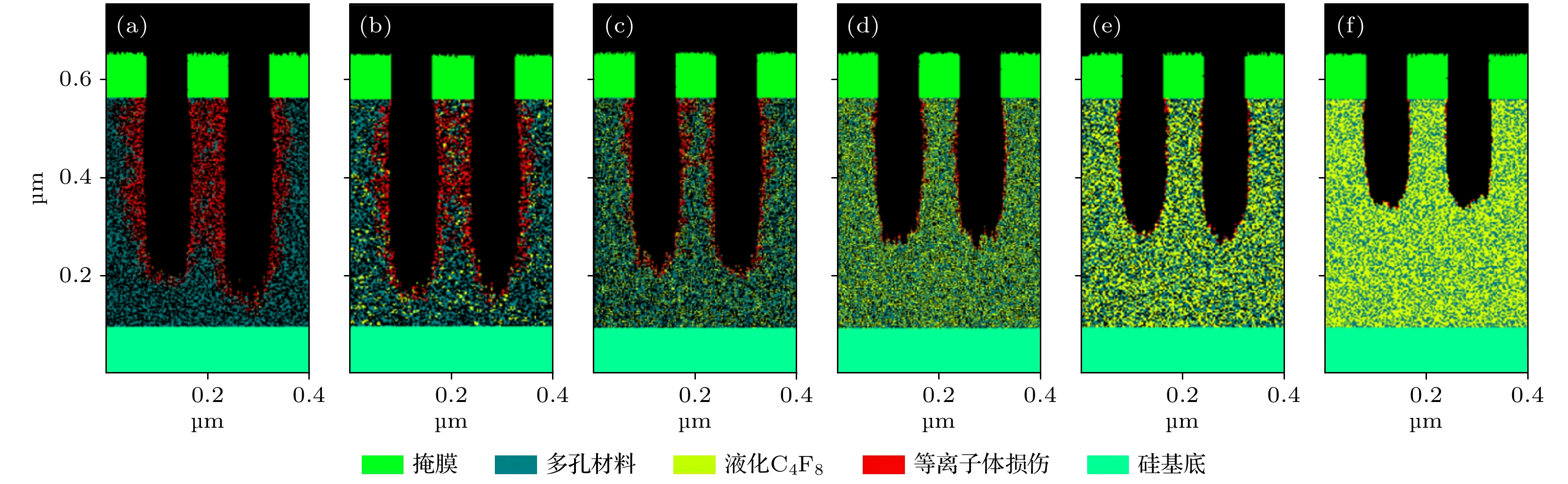


图 16 SF6/C4F8等离子体刻蚀多孔材料的截面结构 (a) –50 ℃刻蚀后结构; (b) –50 ℃刻蚀后浸到dHF酸溶液30 s; (c) –110 ℃刻蚀后结构; (d) –110 ℃刻蚀后浸到dHF酸溶液30 s[24]
Fig. 16. Cross-sectional images of narrow spacing trench profiles: (a) –50 ℃, after plasma etching; (b) –50 ℃, after plasma etching and 0.5% dHF dip 30 s; (c) –110 ℃, after plasma etching; (d) –110 ℃, after plasma etching and 0.5% dHF dip 30 s [24].
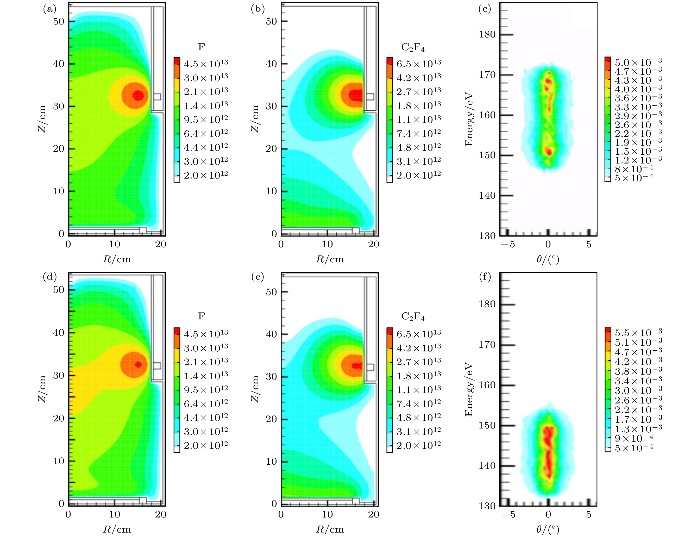
图 17 低温刻蚀–50 ℃时, (a) F密度分布, (b) C2F4自由基分布, (c)离子能量分布; 低温刻蚀–120 ℃时, (d) F密度分布, (e) C2F4自由基分布, (f)离子能量分布[24]
Fig. 17. Calculated (a) and (d) F atom density (in cm–3), (b) and (e) C2F4 molecule density (in cm–3), and (c) and (f) normalized ion energy and angular distributions, at –50 ℃ (a)–(c) and –120 ℃ (d)–(f)[24]
-
[1] Sicard E, Boyer A 2019 EMC Compo Haining, China, October 21–23, 2019 ffhal-02403882
[2] [3] 王婷婷, 叶超, 宁兆元, 程珊华 2005 物理学报 54 892
Google Scholar
Wang T T, Ye C, Ning Z Y, Cheng S H 2005 Acta Phys. Sin. 54 892
Google Scholar
[4] Zhang L, Marneffe J F, Heyne M, Naumov S, Sun Y T, et al. 2015 ECS J. Solid State Sci. Technol. 4 N3098
Google Scholar
[5] Baklanov M, Marneffe J F, Shamiryan D, Urbanowicz A, Shi H, Rakhimova T, Huang H, Ho P 2013 J. Appl. Phys. 113 041101
Google Scholar
[6] Lionti K, Volksen W, Magbitang T, Darnon M, Dubois G 2015 ECS J. Solid State Sci. Technol. 4 N3071
Google Scholar
[7] Frot T, Volksen W, Purushothaman S, Bruce R, Dubois G 2011 Adv. Mater. 23 2828
Google Scholar
[8] Frot T, Volksen W, Purushothaman S, Bruce R L, Magbitang T, Miller D C, Deline V R, Dubois G 2012 Adv. Funct. Mater. 22 3043
Google Scholar
[9] Tachi S, Tsujimoto K, Okudaira S 1988 Appl. Phys. Lett. 52 616
Google Scholar
[10] Tachi S, Tsujimoto K, Arai S, Kure T 1991 J. Vac. Sci. Technol., A 9 796
Google Scholar
[11] Tsujimoto K, Okudaira S, Tachi S 1991 Jpn. J. Appl. Phys. 30 3319
Google Scholar
[12] Zhang L, Ljazouli R, Lefaucheux P, Tillocher T, Dussart R, Mankelevich Y A, de Marneffe J F, de Gendt S, Baklanov M R 2013 ECS Solid State Lett. 2 N5
Google Scholar
[13] Zhang L, Ljazouli R, Lefaucheux P, Tillocher T, Dussart R, Mankelevich Y A, de Marneffe J F, de Gendt S, Baklanov M R 2013 ECS J. Solid State Sci. Technol. 2 N131
Google Scholar
[14] Zhang L, de Marneffe J F, Leroy F, Lefaucheux P, Tillocher T, Dussart R, Maekawa K, Yatsuda K, Dussarrat C, Goodyear A, Cooke M, De Gendt S, Baklanov M R 2016 J. Phys. D: Appl. Phys. 49 175203
Google Scholar
[15] Dussart R, Tillocher T, Lefaucheux P, Boufnichel M 2014 J. Phys. D: Appl. Phys. 47 123001
Google Scholar
[16] Chanson R, Zhang L, Naumov S, Mankelevich Yu A, Tillocher T, Lefaucheux P, Dussart R, De Gendt S, De Marneffe J F 2018 Sci. Rep. 8 1886
Google Scholar
[17] Chanson R, Tahara S, Vanstreels K, de Marneffe J F 2018 Plasma Research Express 1 015006
Google Scholar
[18] Chanson R, Dussart R, Tillocher T, Lefaucheux P, Dussarrat C, De Marneffe J F 2019 Front. Chem. Sci. Eng. 13 511
Google Scholar
[19] Rezvanov A, Miakonkikh A, Vishnevskiy A, Rudenko K, Baklanov M 2017 J. Vac. Sci. Technol. B 35 021204
Google Scholar
[20] Kushner M 2009 J. Phys. D: Appl. Phys. 42 194013
Google Scholar
[21] Sankaran A, Kushner M J 2004 Vac. Sci. Technol., A 22 1242
[22] 胡艳婷, 张钰如, 宋远红, 王友年 2018 物理学报 67 225203
Google Scholar
Hu Y T, Zhang Y R, Song Y H, Wang Y N 2018 Acta Phys. Sin. 67 225203
Google Scholar
[23] 蒋相占, 刘永新, 毕振华, 陆文琪, 王友年 2012 物理学报 61 015204
Google Scholar
Jiang X Z, Liu Y X, Bi Z H, Lu W Q, Wang Y N 2012 Acta Phys. Sin. 61 015204
Google Scholar
[24] Zhang Q Z, Tink S, De Marneffe J F, Zhang L P, Bogaerts A 2017 Appl. Phys. Lett. 111 173104
Google Scholar
[25] Zhang Q Z, Jiang W, Hou L J, Wang Y N 2011 J. Appl. Phys. 109 013308
Google Scholar

 下载:
下载:
计量
- 文章访问数: 11008
- PDF下载量: 244
- 被引次数: 0
