


-
研究9,9′-二亚呫吨分子在Ru(0001)上的吸附行为, 在室温下通过扫描隧道电子显微镜观察石墨烯的自下而上制备过程. 在亚单层体系中, 9,9′-二亚呫吨分子随机吸附在Ru(0001)上, 简单分析了其空间结构; 并以 9,9′-二亚呫吨分子为前体, 在Ru(0001)衬底上自下而上制备石墨烯, 在超高真空中对Ru(0001)衬底进行长时间退火后, 首次发现其具有3种不同旋转角(6.3°, 13.9°和16.1°)的摩尔超结构, 迄今为止未见报道, 并通过构建模型分析这3种摩尔超结构的形成机制. 本实验为丰富Ru(0001)上摩尔超结构多样性作出了贡献, 同时也对以石墨烯/Ru(0001)为基的科学研究打下基础.This paper reports the adsorption behavior of the 9,9′-Dixanthylidene on Ru(0001), the bottom-up fabrication of graphene is also investigated through a scanning tunneling microscope (STM). We analyze the spatial structure of 9,9′-Dixanthylidene molecules which are randomly dispersed on a Ru(0001) substrate in the sub-monolayer coverage. Then we bottom-up fabricate the graphene on the Ru(0001) substrate with the 9,9′-Dixanthylidene molecules as the precursor. Three kinds of moiré superstructures with different rotation angles (6.3°, 13.9°, and 16.1°) are found after implementing high temperature annealing in ultrahigh vacuum. This result provides data support for the study of moiré superstructures on Ru(0001) substrate and lays a solid foundation for further scientific research based on graphene/Ru(0001).
-
Keywords:
- 9,9′-Dixanthylidene /
- graphene /
- Ru(0001) /
- scanning tunneling microscopy
[1] Berger C, Song Z M, Li X B, Wu X S, Brown N, Naud C, Mayou D, Li T B, Hass J, Marchenkov A N, Conrad E H, First P N, de Heer W A 2006 Science 312 1191
 Google Scholar
[2] Novoselov K S, Geim A K, Morozov S V, Jiang D, Zhang Y, Dubonos S V, Grigorieva I V, Firsov A A 2004 Science 306 666
Google Scholar
[3] Yi M, Shen Z G 2015 J. Mater. Chem. A 3 11700
Google Scholar
[4] Li X S, Cai W W, An J H, Kim S, Nah J, Yang D X, Piner R, Velamakanni A, Jung I, Tutuc E, Banerjee S K, Colombo L, Ruoff R S 2009 Science 324 1312
Google Scholar
[5] Sun Z Z, Yan Z, Yao J, Beitler E, Zhu Y, Tour J M 2010 Nature 468 549
Google Scholar
[6] Li Z C, Wu P, Wang C X, Fan X D, Zhang W H, Zhai X F, Zeng C G, Li Z Y, Yang J L, Hou J G 2011 ACS Nano 5 3385
Google Scholar
[7] Chen Q Y, Song J J, Jing L W, Huang K K, He P M, Zhang H J 2020 Chin. Phys. B 29 026801
Google Scholar
[8] Song J J, Zhang H J, Zhang Y X, Cai Y L, Bao S N, He P M 2016 Appl. Surf. Sci. 367 424
Google Scholar
[9] Zhang H J, Lü B, Lu Y H, Huang H, Li H Y, Bao S N, He P M 2006 Chin. Phys. 15 1892
Google Scholar
[10] N'Diaye A T, Bleikamp S, Feibelman P J, Michely T 2006 Phys. Rev. Lett. 97 215501
Google Scholar
[11] Hattab H, N’Diaye A T, Wall D, Jnawali G, Coraux J, Busse C, van Gastel R, Poelsema B, Michely T, Meyer zu Heringdorf F J, Horn-von Hoegen M 2011 Appl. Phys. Lett. 98 141903
Google Scholar
[12] Ueta H, Saida M, Nakai C, Yamada Y, Sasaki M, Yamamoto S 2004 Surf. Sci. 560 183
Google Scholar
[13] Sutter P W, Flege J I, Sutter E A 2008 Nat. Mater. 7 406
Google Scholar
[14] Wang B, Bocquet M L, Marchini S, Gunther S, Wintterlin J 2008 Phys. Chem. Chem. Phys. 10 3530
Google Scholar
[15] Martoccia D, Willmott P R, Brugger T, Björck M, Günther S, Schlepütz C M, Cervellino A, Pauli S A, Patterson B D, Marchini S, Wintterlin J, Moritz W, Greber T 2008 Phys. Rev. Lett. 101 126102
Google Scholar
[16] Vázquez de Parga A L, Calleja F, Borca B, Passeggi M C G, Hinarejos J J, Guinea F, Miranda R 2008 Phys. Rev. Lett. 100 056807
Google Scholar
[17] Zhang L N, Dong J C, Guan Z Y, Zhang X Y, Ding F 2020 Nanoscale 12 12831
Google Scholar
[18] Wang B, Bocquet M L 2012 Nanoscale 4 4687
Google Scholar
[19] Zhang L Z, Du S X, Sun J T, Huang L, Meng L, Xu W Y, Pan L D, Pan Y, Wang Y L, Hofer W A, Gao H J 2014 Adv. Mater. Interfaces 1 1300104
Google Scholar
[20] Han Y and Evans J W 2015 J. Chem. Phys. 143 164706
Google Scholar
[21] Juan D A, Mariano D J S, Jose M G R 2019 J. Phys. Chem. C 123 5525
Google Scholar
[22] Ren J D, Guo H M, Pan J B, Zhang Y F, Yang Y F, Wu X, Du S X, Ouyang M, Gao H J 2017 Phys. Rev. Lett. 119 176806
Google Scholar
[23] 张志模, 张文号, 付英双 2019 物理学报 68 226801
Google Scholar
Zhang Z M, Zhang W H, Fu Y S 2019 Acta Phys. Sin. 68 226801
Google Scholar
[24] Peng J P, Zhang H M, Song C L, Jiang Y P, Wang L L, He K, Xue Q K, Ma X C 2015 Chin. Phys. Lett. 32 068104
Google Scholar
[25] Horcas I, Fernández R, Gomez-Rodriguez J M, Colchero G, Baro A M 2007 Rev. Sci. Instrum. 78 013705
Google Scholar
[26] Lu B, Zhang H J, Tao Y S, Huang H, Li H Y, Bao S N, He P, Chen Q 2005 Appl. Phys. Lett. 86 061915
Google Scholar
[27] Cui Y, Fu Q, Zhang H, Bao X H 2011 Chem. Commun. 47 1470
Google Scholar
[28] Bacon M, Bradley S J, Nann T 2014 Part. Part. Syst. Charact. 31 415
Google Scholar
[29] Feng W, Lei S L, Li Q X, Zhao A D 2011 J. Phys. Chem. C 115 24858
Google Scholar
[30] Jiang D E, Du M H, Dai S 2009 J. Chem. Phys. 130 074705
Google Scholar
[31] Thiemann F L, Rowe P, Zen A, Muller E A, Michaelides A 2021 Nano Lett. 21 8143
Google Scholar
[32] Bhattarai B, Biswas P, Raymond A F, Drabold D A 2018 Phys. Chem. Chem. Phys. 20 19546
Google Scholar
[33] Kumar A, Wilson M, Thorpe M F 2012 J. Phys. Condens. Matter 24 485003
Google Scholar
[34] Yan Y B, Gong J, Chen J, Zeng Z P, Huang W, Pu K Y, Liu J Y and Chen P 2019 Adv. Mater. 31 1808283
Google Scholar
[35] Ye R Q, Peng Z W, Metzger A, Lin J, Mann J A, Huang K W, Xiang C S, Fan X J, Samuel E L G, Alemany L B, Martí A A, Tour J M 2015 ACS Appl. Mater. Interfaces. 7 7041
Google Scholar
[36] Tomanek D, Louie S G, Mamin H J, Abraham D W, Thomson R E, Ganz E, Clarke J 1987 Phys. Rev. B 35 7790
Google Scholar
[37] Wan X, Chen K, Liu D Q, Chen J, Miao Q, Xu J B 2012 Chem. Mater. 24 3906
Google Scholar
[38] Talirz L, Ruffieux P, Fasel R 2016 Adv. Mater. 28 6222
Google Scholar
[39] Talirz L, Söde H, Cai J M, Ruffieux P, Blankenburg S, Jafaar R, Berger R, Feng X L, Müllen K, Passerone D, Fasel R, Pignedoli C A 2013 J. Am. Chem. Soc. 135 2060
Google Scholar
[40] Jing L W, Song J J, Zhang Y X, Chen Q Y, Huang K K, Zhang H J, He P M 2019 Chin. Phys. B 28 076801
Google Scholar
[41] N'Diaye A T, Coraux J, Plasa T N, Busse C, Michely T 2008 New J. Phys. 10 043033
Google Scholar
-
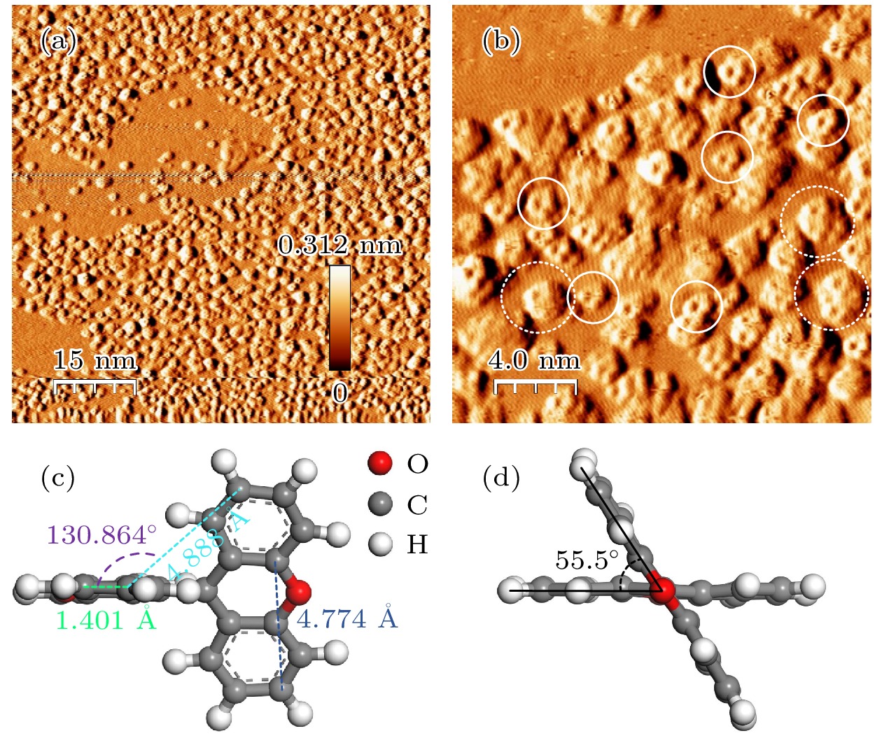
图 1 (a) 大量9,9′-二亚呫吨分子吸附于Ru(0001)上的STM图(
$75\;{\rm nm}\times75\;{\rm nm} $ , 隧穿电压${V}_{\mathrm{T}}=-0.093\;\rm{V} $ , 隧穿电流${I}_{\mathrm{T}}=0.465\;\rm{n}\mathrm{A} $ ); (b) 9,9′-二亚呫吨分子的高清STM图$\left(20\;{\rm nm\times 20\; nm}, \;{V}_{\mathrm{T}}=-0.002\;{\rm V},\; {I}_{\mathrm{T}}=0.285\;\rm{nA}\right)$ , 白色实线圆圈指出有机分子, 白色虚线圆圈指出了石墨烯量子点; (c) 9,9′-二亚呫吨分子模型的正视图和一些参数标识; (d) 9,9′-二亚呫吨分子模型的侧视图Fig. 1. (a) STM image of a large number of 9,9′-Dixanthylidene molecules on Ru(0001)(
$75\;{\rm nm}\times75\;{\rm nm} $ ,${V}_{\mathrm{T}}= $ $ -0.093\;\rm{V}$ ,${I}_{\mathrm{T}}=0.465\;\rm{n}\mathrm{A} $ ); (b) high-resolution-STM image of 9,9′-Dixanthylidene molecules$\left(20\;{\rm nm}\times 20\;{\rm nm},\; {V}_{\mathrm{T}}= $ $ -0.002\;\rm{V},\; {I}_{\mathrm{T}}=0.285\;\rm{n}\mathrm{A}\right)$ , the white solid circles indicate the molecules, and the white dashed circles indicate the graphene quantum dots; (c) front view of 9,9′-Dixanthylidene molecular simulation diagram and display of necessary parameters; (d) side view of 9,9′-Dixanthylidene molecule simulation diagram.
图 2 (a) 9,9'-二亚呫吨分子分布在未定型石墨烯上的STM图
$(20\;\mathrm{nm}\times20\;\mathrm{nm},\; {V}_{\mathrm{T}}=-0.099\;{\rm V},\; {I}_{\mathrm{T}}=0.403\;\rm{n}\mathrm{A})$ ; (b) 图(a)周边的STM扫描图$(20\;\mathrm{nm}\times20\;\mathrm{nm},\; {V}_{\mathrm{T}}=-0.051\;{\rm V},\; {I}_{\mathrm{T}}=0.683\;\mathrm{nA})$ ; (c) 9,9'-二亚呫吨分子在未定型石墨烯上的模拟吸附形态; (d) 图(a)中蓝色区域的放大图像, a和b分别代表图(d)测量间距的两个碳环$(5\;\mathrm{nm}\times5\;\mathrm{nm},\; {V}_{\mathrm{T}}=-0.099\;{\rm V},\; {I}_{\mathrm{T}}=0.403\;\rm{n}\mathrm{A})$ ; (e) 图(d)中沿绿线的高度分布图; (f) 图(d)中沿蓝线的高度分布图Fig. 2. (a) STM image of 9,9'-Dixanthylidene molecules on the amorphous graphene
$(20\;\mathrm{nm}\times20\;\mathrm{nm},\; {V}_{\mathrm{T}}=-0.099\;{\rm V},\; {I}_{\mathrm{T}}=0.403\;\mathrm{nA})$ ; (b) STM image of the around area of panel (a)$\left(20\;\mathrm{nm}\times 20\;\mathrm{nm},\; {V}_{\rm T}=-0.051\;{\rm V}, \;{I}_{\rm T}=0.683\;{\rm nA}\right);$ (c) the simulated tiled morphology of the 9,9'-Dixanthylidene molecule in panel (a); (d) enlarged image of the blue rectangle in panel (a), a and b represent the two carbon rings that measured the distance in panel (d) respectively$(5\;\mathrm{nm}\times5\;\mathrm{nm},\; {V}_{\mathrm{T}}=-0.099\;{\rm V},\; {I}_{\mathrm{T}}=0.403\;\mathrm{nA})$ ; (e) line profile along the green line outlined in panel (d); (f) line profile along the blue line outlined in panel (d).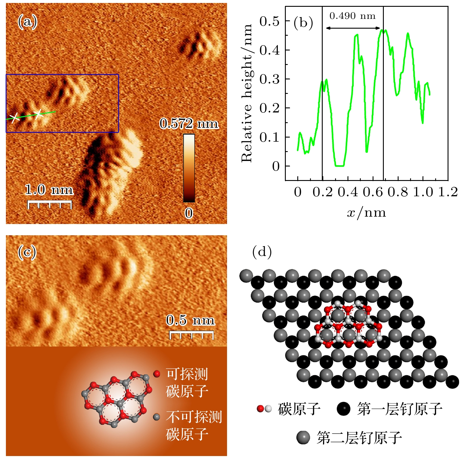
图 3 (a) 石墨烯量子点的STM图
$\left(5\;\mathrm{nm}\times 5\;\mathrm{nm},\; {V}_{\mathrm{T}}= $ $ -0.002\;{\rm V}, \; {I}_{\mathrm{T}}=0.149\;\rm{n}\mathrm{A}\right);$ (b) 图(a)中沿绿线的高度分布图; (c) 图(a) 中蓝框处的更高清的STM图$(2.5\;\mathrm{nm}\times2.5\;\mathrm{nm}, $ $ {V}_{\mathrm{T}}=-0.002\;{\rm V},\; {I}_{\mathrm{T}}=0.263\;\mathrm{nA})$ , 石墨烯量子点的球棍模型被展示在图片的下方; (d) 5C6型石墨烯量子点吸附在Ru(0001)上的理论模型(红色圆球代表扫描过程中扫描到的碳原子, 白色圆球代表扫描不到的碳原子; 黑色原子代表Ru(0001)上第一层的钌原子, 灰色原子代表第二层的钌原子)Fig. 3. (a) STM image of graphene quantum dots
$\left(5\;\mathrm{nm}\times $ $ 5\;\mathrm{nm},\; {V}_{\mathrm{T}}=-0.002\;{\rm V},\; {I}_{\mathrm{T}}=0.149\;\rm{n}\mathrm{A}\right)$ ; (b) line profile along the green line outlined in panel (a); (c) high-resolution STM image of the blue rectangle area in panel (a), showing the graphene quantum dots in detail$(2.5\;\mathrm{nm}\times2.5\;\mathrm{nm},\; {V}_{\mathrm{T}}= $ $ -0.002\;{\rm V}, \; {I}_{\mathrm{T}}=0.263\;\rm{n}\mathrm{A})$ , the ball-and-stick model of graphene quantum dot is displayed; (d) theoretical simulation image of 5C6 graphene quantum dots adsorbed on the Ru(0001) substrate (the red spheres are visible atoms, the white spheres are invisible atoms, the black atoms are the atoms of the first layer of the ruthenium substrate, and the gray atoms are the atoms of the second layer of the ruthenium substrate).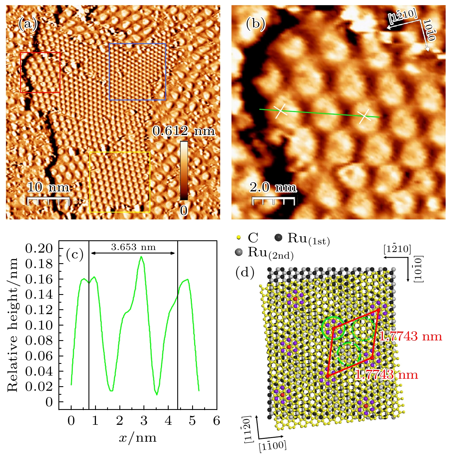
图 4 (a) Ru(0001)衬底上3种摩尔超结构的STM图
$(50\; \mathrm{nm}\times 50\;\mathrm{nm},\; {V}_{\mathrm{T}}=-0.401\;{\rm V},\; {I}_{\mathrm{T}}=0.258\;\mathrm{nA});$ (b) 图(a)中红框区域的摩尔超结构图(6.3°的摩尔超结构)$\left(10\;\mathrm{nm}\times $ $ 10\;\mathrm{nm},\; {V}_{\mathrm{T}}=-0.401\;{\rm V},\; {I}_{\mathrm{T}}=0.258\;\mathrm{nA}\right)$ ; (c) 图(b)中绿线的高度分布图; (d) 石墨烯与Ru(0001)衬底成6.3°夹角的摩尔超结构模拟图(其中黑色圆球代表衬底第一层钌原子, 灰色圆球代表衬底第二层钌原子, 黄色部分为石墨烯)Fig. 4. (a) STM image of three kinds of moiré superstructures on Ru(0001) substrate
$\left(50\;{\rm n}\mathrm{m}\times 50\;{\rm n}\mathrm{m},\; {V}_{\mathrm{T}}= -0.401\;{\rm V}, $ $ \; {I}_{\mathrm{T}}=0.258\;{\rm n}\mathrm{A}\right);$ (b) STM topography of the red rectangle area in panel (a) which is the moiré superstructure of graphene on Ru (0001) with the angle of 6.3°$\left(10\;{\rm n}\mathrm{m}\times 10\;{\rm n}\mathrm{m}, $ $ \; {V}_{\mathrm{T}}=-0.401\;{\rm V},\; {I}_{\mathrm{T}}=0.258\;{\rm n}\mathrm{A}\right)$ ; (c) line profile along the green line outlined in panel (b); (d) the simulated image of graphene at a 6.3° angle to the ruthenium substrate (the black balls represent the first layer of ruthenium atoms, the gray balls represent the second layer of ruthenium atoms, and yellow small balls represent carbon atoms).
图 5 (a) 图4(a)中蓝框区域的摩尔超结构图(13.9°的摩尔超结构)
$\left(15\;{\rm nm}\times 15\;{\rm nm},\; {V}_{\mathrm{T}}=-0.401\;{\rm V},\; I_{\mathrm{T}}=0.258\;\rm{n A}\right);$ (b) 图(a)中沿绿线的高度分布图; (c) 石墨烯与Ru(0001)衬底成13.9°夹角的摩尔超结构模拟图(其中黑色圆球代表衬底第1层钌原子, 灰色圆球代表衬底第2层钌原子, 黄色部分为石墨烯)Fig. 5. (a) STM topography of the blue rectangle area in Fig. 4(a) which is the superstructure of graphene on Ru (0001) with an angle of 13.9°
$\left(15\;{\rm nm}\times 15\;{\rm n m},\; {V}_{\rm{T}}=-0.401\;{\rm V},\; {I}_{\rm{T}}=0.258\;\rm{n}\rm{A}\right);$ (b) line profile along the green line outlined in panel (a); (c) the simulated image of the superstructure at a 13.9° angle to the ruthenium substrate, the unit cell is highlighted by the red rhombus (the black balls represent the first layer of ruthenium atoms, the gray balls represent the second layer of ruthenium atoms, and yellow small balls represent carbon atoms).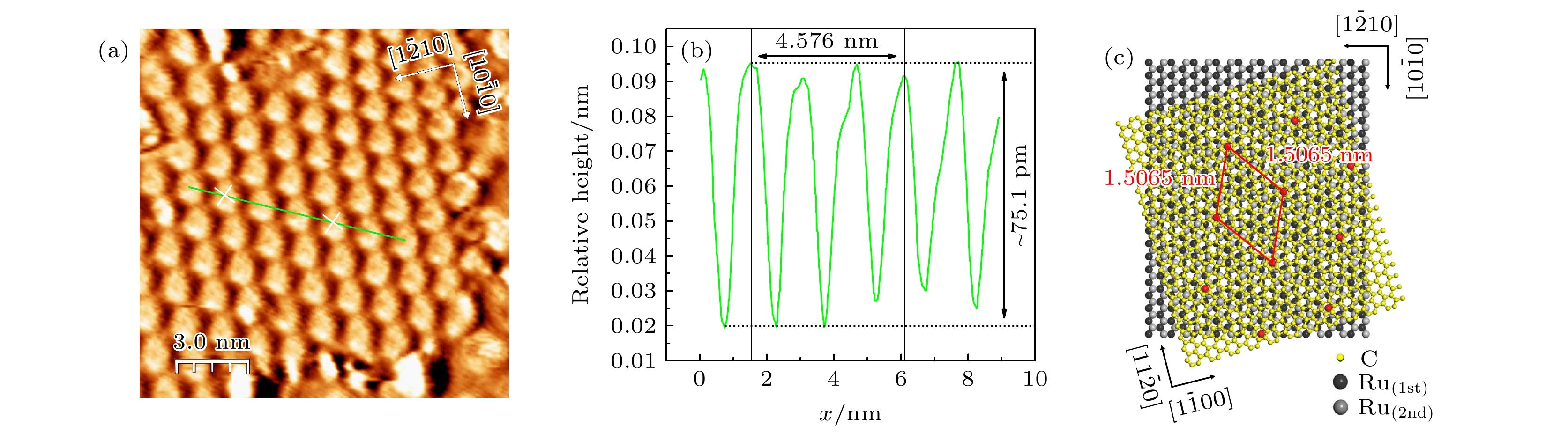
图 6 (a) 图4(a)中黄框区域的摩尔超结构图(16.1°的摩尔超结构)
$(15\;{\rm nm \times 15\; nm},\; {V}_{\mathrm{T}}=-0.401\;{\rm V},\; {I}_{\mathrm{T}}=0.258\;\rm{nA})$ ; (b) 图(a)中沿着绿线的高度分布图; (c) 石墨烯与Ru(0001)衬底成16.1°夹角的摩尔超结构模拟图(其中黑色圆球代表衬底第一层钌原子, 灰色圆球代表衬底第二层钌原子, 黄色部分为石墨烯)Fig. 6. (a) STM topography of the yellow rectangle area in Fig. 4(a) which is the moiré superstructure of graphene on Ru (0001) with an angle of 16.1°
$\left(15\;{\rm n}\mathrm{m}\times 15\;{\rm n}\mathrm{m},\; {V}_{\mathrm{T}}=-0.401\;{\rm V},\; {I}_{\mathrm{T}}=0.258\;\rm{n}\mathrm{A}\right)$ ; (b) line profile along the green line outlined in panel (a); (c) the corresponding structural model, the unit cell is also highlighted by the red rhombus (the black balls represent the first layer of ruthenium atoms, the gray balls represent the second layer of ruthenium atoms, and yellow small balls represent carbon atoms). -
[1] Berger C, Song Z M, Li X B, Wu X S, Brown N, Naud C, Mayou D, Li T B, Hass J, Marchenkov A N, Conrad E H, First P N, de Heer W A 2006 Science 312 1191
Google Scholar
[2] Novoselov K S, Geim A K, Morozov S V, Jiang D, Zhang Y, Dubonos S V, Grigorieva I V, Firsov A A 2004 Science 306 666
Google Scholar
[3] Yi M, Shen Z G 2015 J. Mater. Chem. A 3 11700
Google Scholar
[4] Li X S, Cai W W, An J H, Kim S, Nah J, Yang D X, Piner R, Velamakanni A, Jung I, Tutuc E, Banerjee S K, Colombo L, Ruoff R S 2009 Science 324 1312
Google Scholar
[5] Sun Z Z, Yan Z, Yao J, Beitler E, Zhu Y, Tour J M 2010 Nature 468 549
Google Scholar
[6] Li Z C, Wu P, Wang C X, Fan X D, Zhang W H, Zhai X F, Zeng C G, Li Z Y, Yang J L, Hou J G 2011 ACS Nano 5 3385
Google Scholar
[7] Chen Q Y, Song J J, Jing L W, Huang K K, He P M, Zhang H J 2020 Chin. Phys. B 29 026801
Google Scholar
[8] Song J J, Zhang H J, Zhang Y X, Cai Y L, Bao S N, He P M 2016 Appl. Surf. Sci. 367 424
Google Scholar
[9] Zhang H J, Lü B, Lu Y H, Huang H, Li H Y, Bao S N, He P M 2006 Chin. Phys. 15 1892
Google Scholar
[10] N'Diaye A T, Bleikamp S, Feibelman P J, Michely T 2006 Phys. Rev. Lett. 97 215501
Google Scholar
[11] Hattab H, N’Diaye A T, Wall D, Jnawali G, Coraux J, Busse C, van Gastel R, Poelsema B, Michely T, Meyer zu Heringdorf F J, Horn-von Hoegen M 2011 Appl. Phys. Lett. 98 141903
Google Scholar
[12] Ueta H, Saida M, Nakai C, Yamada Y, Sasaki M, Yamamoto S 2004 Surf. Sci. 560 183
Google Scholar
[13] Sutter P W, Flege J I, Sutter E A 2008 Nat. Mater. 7 406
Google Scholar
[14] Wang B, Bocquet M L, Marchini S, Gunther S, Wintterlin J 2008 Phys. Chem. Chem. Phys. 10 3530
Google Scholar
[15] Martoccia D, Willmott P R, Brugger T, Björck M, Günther S, Schlepütz C M, Cervellino A, Pauli S A, Patterson B D, Marchini S, Wintterlin J, Moritz W, Greber T 2008 Phys. Rev. Lett. 101 126102
Google Scholar
[16] Vázquez de Parga A L, Calleja F, Borca B, Passeggi M C G, Hinarejos J J, Guinea F, Miranda R 2008 Phys. Rev. Lett. 100 056807
Google Scholar
[17] Zhang L N, Dong J C, Guan Z Y, Zhang X Y, Ding F 2020 Nanoscale 12 12831
Google Scholar
[18] Wang B, Bocquet M L 2012 Nanoscale 4 4687
Google Scholar
[19] Zhang L Z, Du S X, Sun J T, Huang L, Meng L, Xu W Y, Pan L D, Pan Y, Wang Y L, Hofer W A, Gao H J 2014 Adv. Mater. Interfaces 1 1300104
Google Scholar
[20] Han Y and Evans J W 2015 J. Chem. Phys. 143 164706
Google Scholar
[21] Juan D A, Mariano D J S, Jose M G R 2019 J. Phys. Chem. C 123 5525
Google Scholar
[22] Ren J D, Guo H M, Pan J B, Zhang Y F, Yang Y F, Wu X, Du S X, Ouyang M, Gao H J 2017 Phys. Rev. Lett. 119 176806
Google Scholar
[23] 张志模, 张文号, 付英双 2019 物理学报 68 226801
Google Scholar
Zhang Z M, Zhang W H, Fu Y S 2019 Acta Phys. Sin. 68 226801
Google Scholar
[24] Peng J P, Zhang H M, Song C L, Jiang Y P, Wang L L, He K, Xue Q K, Ma X C 2015 Chin. Phys. Lett. 32 068104
Google Scholar
[25] Horcas I, Fernández R, Gomez-Rodriguez J M, Colchero G, Baro A M 2007 Rev. Sci. Instrum. 78 013705
Google Scholar
[26] Lu B, Zhang H J, Tao Y S, Huang H, Li H Y, Bao S N, He P, Chen Q 2005 Appl. Phys. Lett. 86 061915
Google Scholar
[27] Cui Y, Fu Q, Zhang H, Bao X H 2011 Chem. Commun. 47 1470
Google Scholar
[28] Bacon M, Bradley S J, Nann T 2014 Part. Part. Syst. Charact. 31 415
Google Scholar
[29] Feng W, Lei S L, Li Q X, Zhao A D 2011 J. Phys. Chem. C 115 24858
Google Scholar
[30] Jiang D E, Du M H, Dai S 2009 J. Chem. Phys. 130 074705
Google Scholar
[31] Thiemann F L, Rowe P, Zen A, Muller E A, Michaelides A 2021 Nano Lett. 21 8143
Google Scholar
[32] Bhattarai B, Biswas P, Raymond A F, Drabold D A 2018 Phys. Chem. Chem. Phys. 20 19546
Google Scholar
[33] Kumar A, Wilson M, Thorpe M F 2012 J. Phys. Condens. Matter 24 485003
Google Scholar
[34] Yan Y B, Gong J, Chen J, Zeng Z P, Huang W, Pu K Y, Liu J Y and Chen P 2019 Adv. Mater. 31 1808283
Google Scholar
[35] Ye R Q, Peng Z W, Metzger A, Lin J, Mann J A, Huang K W, Xiang C S, Fan X J, Samuel E L G, Alemany L B, Martí A A, Tour J M 2015 ACS Appl. Mater. Interfaces. 7 7041
Google Scholar
[36] Tomanek D, Louie S G, Mamin H J, Abraham D W, Thomson R E, Ganz E, Clarke J 1987 Phys. Rev. B 35 7790
Google Scholar
[37] Wan X, Chen K, Liu D Q, Chen J, Miao Q, Xu J B 2012 Chem. Mater. 24 3906
Google Scholar
[38] Talirz L, Ruffieux P, Fasel R 2016 Adv. Mater. 28 6222
Google Scholar
[39] Talirz L, Söde H, Cai J M, Ruffieux P, Blankenburg S, Jafaar R, Berger R, Feng X L, Müllen K, Passerone D, Fasel R, Pignedoli C A 2013 J. Am. Chem. Soc. 135 2060
Google Scholar
[40] Jing L W, Song J J, Zhang Y X, Chen Q Y, Huang K K, Zhang H J, He P M 2019 Chin. Phys. B 28 076801
Google Scholar
[41] N'Diaye A T, Coraux J, Plasa T N, Busse C, Michely T 2008 New J. Phys. 10 043033
Google Scholar


 下载:
下载:


计量
- 文章访问数: 6298
- PDF下载量: 46
- 被引次数: 0
