-
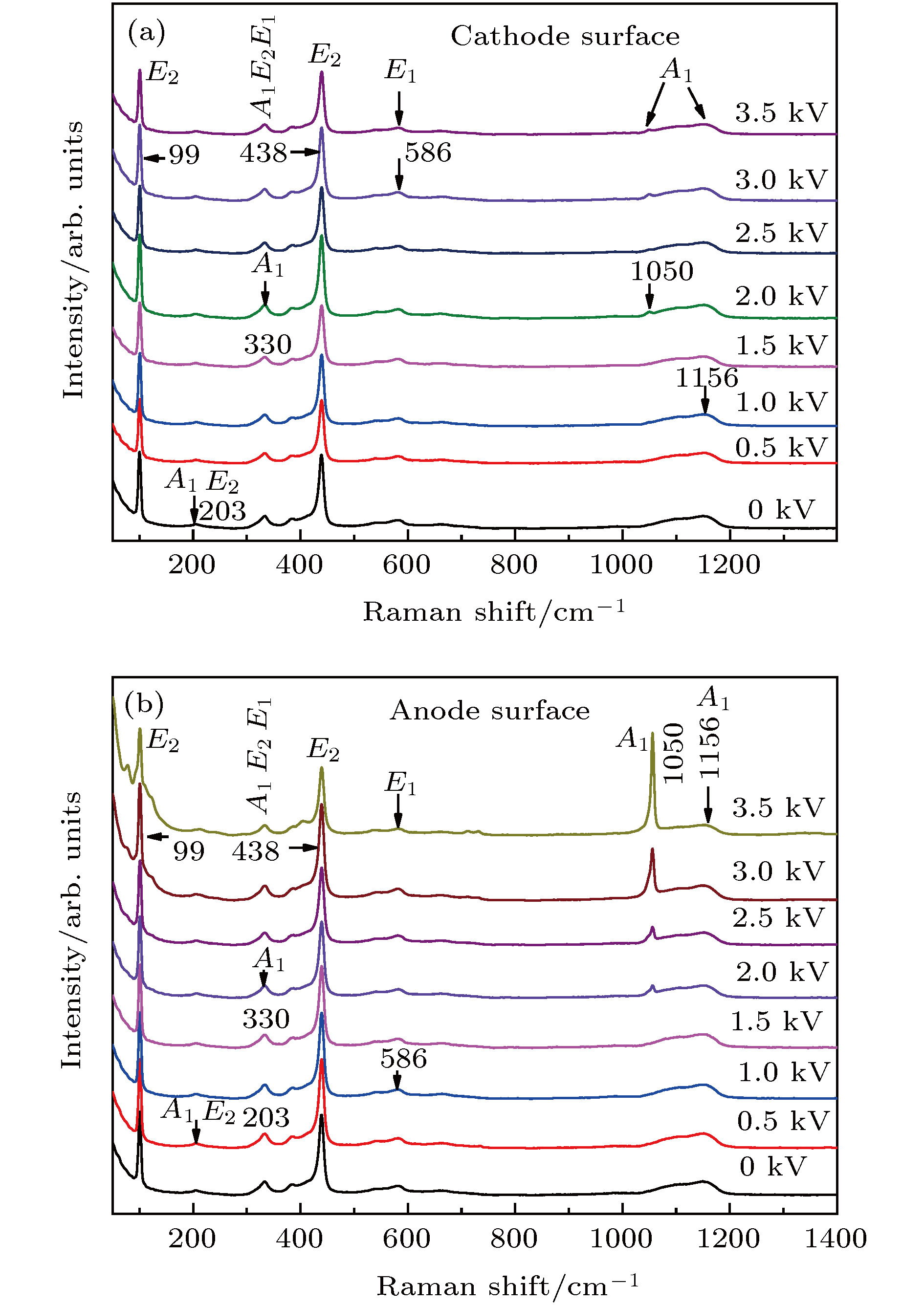
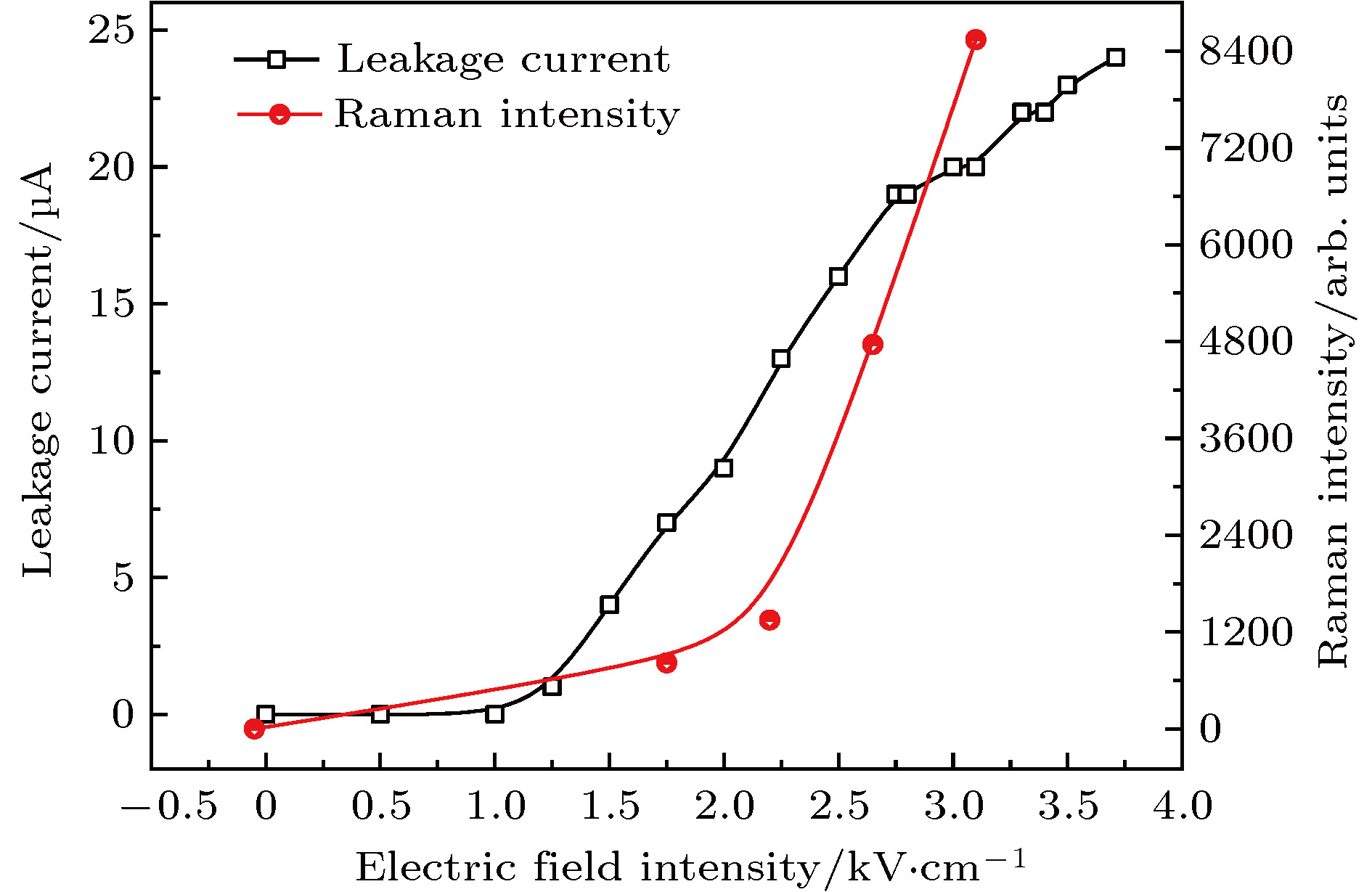
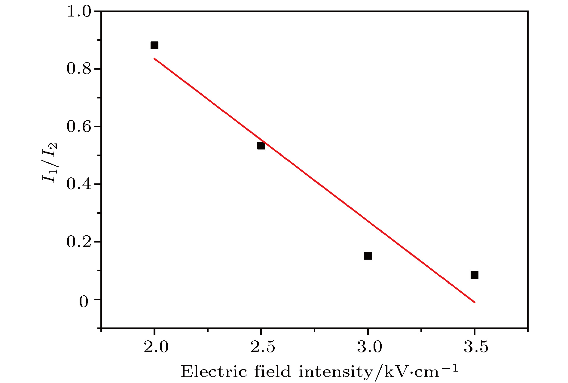
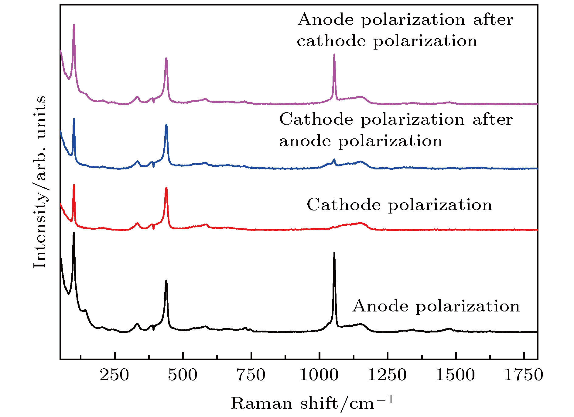
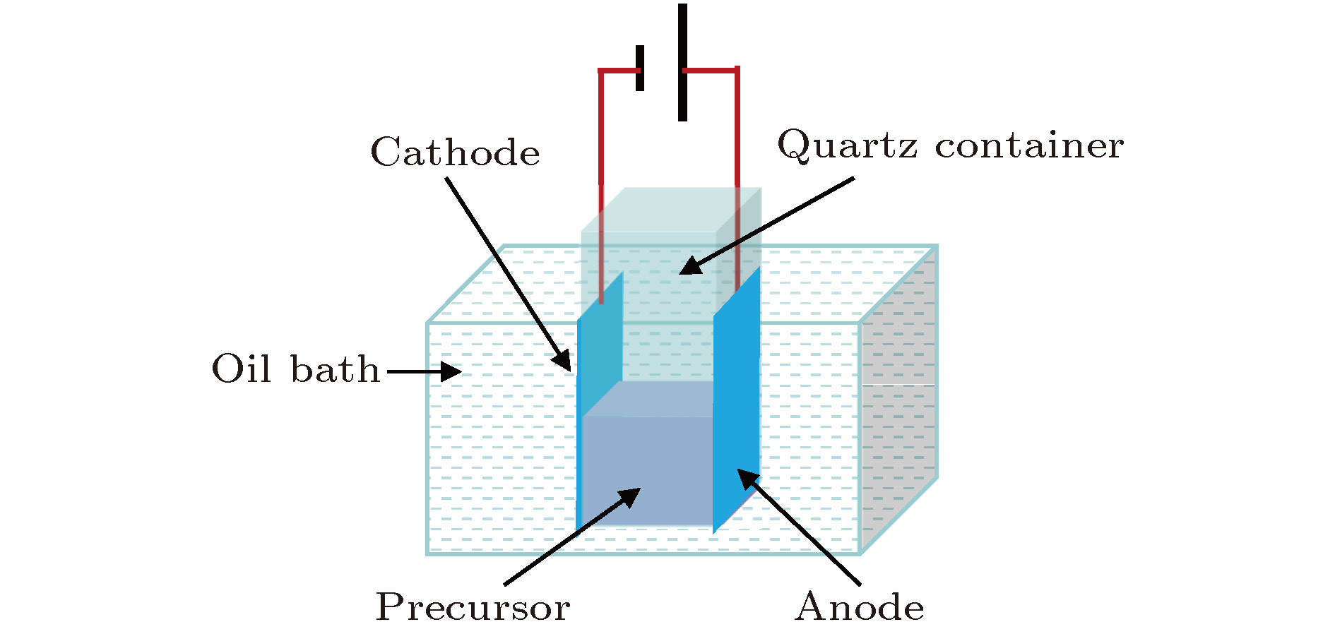
开展高压电场调控纳米材料结构形貌和性能研究在功能材料领域具有重要的理论和实际意义. 本文在高压电场条件下合成了氧化锌纳米粉体, 并对粉末试片进行了后期电场极化处理, 研究了电场对氧化锌的结构形貌、点缺陷、拉曼光谱的影响. 以X射线衍射仪(XRD)、扫描电镜(SEM)和拉曼光谱仪对产物的结构形貌、拉曼位移、缺陷分布等进行了表征. 结果表明, 高压电场条件下氧化锌的完全晶化时间和温度比未施加电场时明显延长和升高, 直流电场能够显著促进前驱物中氧化锌的形核, 并降低晶化速度. 不同电场强度下氧化锌具有不同的显微形貌. 纳米氧化锌粉末试片在直流电场中极化后, 其阴极面和阳极面的拉曼光谱表现出明显的差异. 有明显漏电电流的情况下, 阳极面在1050 cm–1处的二级光学声子模A1(LO)的强度显著提高, 且拉曼强度I1 = 438 cm–1和I2 = 1050 cm–1的比值与极化电场的场强呈线性关系. 当调转试片正反面进行二次极化时, 原来在阳极面尖锐的1050 cm–1峰经过阴极极化而消失. 阳极面1050 cm–1拉曼峰的锐化与氧化锌晶粒内的缺陷重新分布和双肖脱基势垒有关.It is of great theoretical and practical significance to study the regulation of the structure, morphology and properties of nanomaterials by using high voltage electric field in the field of functional materials. Here, ZnO nanocrystalline powders are synthesized under the condition of high voltage electric field. The effect of electric field on the structure, point defect and Raman spectrum of ZnO is studied.The structure, Raman shift and defect distribution of the product are characterized by (XRD), scanning electron microscope (SEM) and Raman spectroscopy (Raman spectroscopy).The results show that the complete crystallization time and temperature of zinc oxide under high voltage electric field are longer and higher than those without electric field. The direct current electric field can significantly promote the nucleation of zinc oxide in the precursor and reduce the rate of crystallization.The morphologies of ZnO obtained under different electric field intensities are obviously different. At a lower electric field intensity, ZnO presents lamellar or stripy morphology that is formed by many 50 nm-diameter nanoparticles. At a higher electric field intensity, ZnO exhibits short conical particles. It can be inferred that the high voltage electric field inhibits the growth of zinc oxide along the c axis (the strongest polar direction).The Raman spectra of the cathode surface and the anode surface showing obvious difference after the nano-ZnO powder has been polarized in the DC electric field.The intensity of the second-order optical phonon mode A1(LO) on the anode surface at 1050 cm–1 increases significantly under the condition of obvious leakage current, and the ratio (I1/I2) of Raman intensity (I1 = 438 cm–1 and I2 = 1050 cm–1) is linearly related to the field strength of the polarized electric field.When the positive and negative sides of the sample disc turn over, the 1050 cm–1 peak increases on the anode surface and tends to disappear on cathode surface.The zinc vacancies with negative charge move toward the anode and the concentration of zinc vacancies on one side of the anode increases significantly, which makes the surface of zinc oxide nanoparticles in the local area of the anode surface exhibit obvious negative electric properties, and increases the local electric field significantly to form a double Shaw base barrier.The Raman shift of 1050 cm–1 belongs to the second order optical phonon A1 (LO) vibrational mode, which is usually in inactive or silent state. When the current passes through, the grain boundary double Schottky barrier is established, which enhances the vibration of the A1 (LO) phonon and increases its Raman frequency shift.It can be concluded that the enhancement of the 1050 cm–1 Raman peak on the anode surface is related to the redistribution of defects in ZnO grains and the double Schottky barrier.
-
Keywords:
- external electric field /
- nano zinc oxide /
- Raman spectra /
- crystallization /
- defect
[1] Zhao L H, Gao Z Y, Zhang J, Lu L W, Zou D S 2018 Appl. Phys. Express 11 115001
 Google Scholar
[2] Singh B K, Tripathi S 2018 J. Lumin. 198 427
 Google Scholar
[3] Savarimuthu K, Sankararajan R, Govindaraj R, Narendhiran S 2018 Nanoscale 10 16022
 Google Scholar
[4] Sivakumar A, Murugesan B, Loganathan A, Sivakumar P 2017 J. Taiwan Inst. Chem. E 78 462
 Google Scholar
[5] Tang X Y, Gao H, Wu L L, Wen J, Pan S M, Liu X, Zhang X T 2015 Chinese Phys. B 24 394
 Google Scholar
[6] Wang S B, Wu Y C, Miao R, Zhang M W, Lu X X, Zhang B, Kinstler A, Ren Z Y, Guo Y B, Lu T F, Suib S L, Gao P X 2017 Cryst. Eng. Comm. 19 5128
 Google Scholar
[7] Sapkota G, Gryczynski K, Mcdougald R, Neogi A, Philipose U 2012 J. Electron Mater. 41 2155
 Google Scholar
[8] Omidvar A 2018 Vacuum 147 126
 Google Scholar
[9] Patterson S, Arora P, Price P, Dittmar J W, Das V K, Pink M, Stein B, Morgan D G, Losovyj Y, Koczkur K M, Skrabalak S E, Bronstein L M 2017 Langmuir 33 14709
 Google Scholar
[10] Meng P F, Yang X, Hu J, He J L 2017 Mater. Lett. 209 413
 Google Scholar
[11] Li Y, Zhao F X, Lian X X 2016 Mater. Sci-Poland 34 708
 Google Scholar
[12] Wu W H, Tang S B, Gu J J, Cao X R 2015 Rsc. Adv. 5 99153
 Google Scholar
[13] Kou L Z, Zhang Y, Li C, Guo W L, Chen C F 2011 J. Phys. Chem. C 115 2381
 Google Scholar
[14] Jammula R K, Srikanth V V S S, Hazra B K, Srinath S 2016 Mater. Design 110 311
 Google Scholar
[15] Gorai P, Seebauer E G 2017 Solid State Ionics 301 95
 Google Scholar
[16] Xue F, Zhang L M, Feng X L, Hu G F, Fan F R, Wen X N, Zheng L, Wang Z L 2015 Nano Res. 8 2390
 Google Scholar
[17] Nakamura T, Nagata T, Hayakawa R, Yoshimura T, Oh S, Hiroshiba N, Chikyow T, Fujimura N, Wakayama Y 2017 Jpn. J. Appl. Phys. 56 032501
 Google Scholar
[18] Li C P, Dai W, Xu S, Li X W, Gao C Y, Chen X M, Yang B H 2015 J. Electron Mater. 44 1095
 Google Scholar
[19] Mikkelsen A, Wojciechowski J, Rajnak M, Kurimsky J, Khobaib K, Kertmen A, Rozynek Z 2017 Materials 10 329
 Google Scholar
[20] Li C, Vaynzof Y, Lakhwani G, Beirne G J, Wang J P, Greenham N C 2017 J. Appl. Phys. 121 144503
 Google Scholar
[21] 安跃华, 熊必涛, 邢云, 申婧翔, 李培刚, 朱志艳, 唐为华 2013 物理学报 62 073103
 Google Scholar
An Y H, Xiong B T, Xing Y, Shen J X, Li P G, Zhu Z Y, Tang W H 2013 Acta Phys. Sin. 62 073103
 Google Scholar
[22] 李酽, 李娇, 陈丽丽, 连晓雪, 朱俊武 2018 物理学报 67 140701
 Google Scholar
Li Y, Li J, Chen L L, Lian X X, Zhu J W 2018 Acta Phys. Sin. 67 140701
 Google Scholar
[23] Hansen M, Truong J, Xie T, Hahm J I 2017 Nanoscal 9 8470
 Google Scholar
[24] Cusco R, Alarcon-Llado E, Ibanez J, Artus L, Jimenez J, Wang B G, Callahan M J 2007 Phys. Rev. B 75 5202
 Google Scholar
[25] Lorite I, Diaz-Carrasco P, Gabas M, Fernandez J F, Costa-Kramer J L 2013 Mater. Lett. 109 167
 Google Scholar
[26] Du G T, Ma Y, Zhang Y T, Yang T P 2005 Appl. Phys. Lett. 87 946
 Google Scholar
-
-
[1] Zhao L H, Gao Z Y, Zhang J, Lu L W, Zou D S 2018 Appl. Phys. Express 11 115001
 Google Scholar
[2] Singh B K, Tripathi S 2018 J. Lumin. 198 427
 Google Scholar
[3] Savarimuthu K, Sankararajan R, Govindaraj R, Narendhiran S 2018 Nanoscale 10 16022
 Google Scholar
[4] Sivakumar A, Murugesan B, Loganathan A, Sivakumar P 2017 J. Taiwan Inst. Chem. E 78 462
 Google Scholar
[5] Tang X Y, Gao H, Wu L L, Wen J, Pan S M, Liu X, Zhang X T 2015 Chinese Phys. B 24 394
 Google Scholar
[6] Wang S B, Wu Y C, Miao R, Zhang M W, Lu X X, Zhang B, Kinstler A, Ren Z Y, Guo Y B, Lu T F, Suib S L, Gao P X 2017 Cryst. Eng. Comm. 19 5128
 Google Scholar
[7] Sapkota G, Gryczynski K, Mcdougald R, Neogi A, Philipose U 2012 J. Electron Mater. 41 2155
 Google Scholar
[8] Omidvar A 2018 Vacuum 147 126
 Google Scholar
[9] Patterson S, Arora P, Price P, Dittmar J W, Das V K, Pink M, Stein B, Morgan D G, Losovyj Y, Koczkur K M, Skrabalak S E, Bronstein L M 2017 Langmuir 33 14709
 Google Scholar
[10] Meng P F, Yang X, Hu J, He J L 2017 Mater. Lett. 209 413
 Google Scholar
[11] Li Y, Zhao F X, Lian X X 2016 Mater. Sci-Poland 34 708
 Google Scholar
[12] Wu W H, Tang S B, Gu J J, Cao X R 2015 Rsc. Adv. 5 99153
 Google Scholar
[13] Kou L Z, Zhang Y, Li C, Guo W L, Chen C F 2011 J. Phys. Chem. C 115 2381
 Google Scholar
[14] Jammula R K, Srikanth V V S S, Hazra B K, Srinath S 2016 Mater. Design 110 311
 Google Scholar
[15] Gorai P, Seebauer E G 2017 Solid State Ionics 301 95
 Google Scholar
[16] Xue F, Zhang L M, Feng X L, Hu G F, Fan F R, Wen X N, Zheng L, Wang Z L 2015 Nano Res. 8 2390
 Google Scholar
[17] Nakamura T, Nagata T, Hayakawa R, Yoshimura T, Oh S, Hiroshiba N, Chikyow T, Fujimura N, Wakayama Y 2017 Jpn. J. Appl. Phys. 56 032501
 Google Scholar
[18] Li C P, Dai W, Xu S, Li X W, Gao C Y, Chen X M, Yang B H 2015 J. Electron Mater. 44 1095
 Google Scholar
[19] Mikkelsen A, Wojciechowski J, Rajnak M, Kurimsky J, Khobaib K, Kertmen A, Rozynek Z 2017 Materials 10 329
 Google Scholar
[20] Li C, Vaynzof Y, Lakhwani G, Beirne G J, Wang J P, Greenham N C 2017 J. Appl. Phys. 121 144503
 Google Scholar
[21] 安跃华, 熊必涛, 邢云, 申婧翔, 李培刚, 朱志艳, 唐为华 2013 物理学报 62 073103
 Google Scholar
An Y H, Xiong B T, Xing Y, Shen J X, Li P G, Zhu Z Y, Tang W H 2013 Acta Phys. Sin. 62 073103
 Google Scholar
[22] 李酽, 李娇, 陈丽丽, 连晓雪, 朱俊武 2018 物理学报 67 140701
 Google Scholar
Li Y, Li J, Chen L L, Lian X X, Zhu J W 2018 Acta Phys. Sin. 67 140701
 Google Scholar
[23] Hansen M, Truong J, Xie T, Hahm J I 2017 Nanoscal 9 8470
 Google Scholar
[24] Cusco R, Alarcon-Llado E, Ibanez J, Artus L, Jimenez J, Wang B G, Callahan M J 2007 Phys. Rev. B 75 5202
 Google Scholar
[25] Lorite I, Diaz-Carrasco P, Gabas M, Fernandez J F, Costa-Kramer J L 2013 Mater. Lett. 109 167
 Google Scholar
[26] Du G T, Ma Y, Zhang Y T, Yang T P 2005 Appl. Phys. Lett. 87 946
 Google Scholar
计量
- 文章访问数: 23427
- PDF下载量: 276
- 被引次数: 0


 下载:
下载:


