-
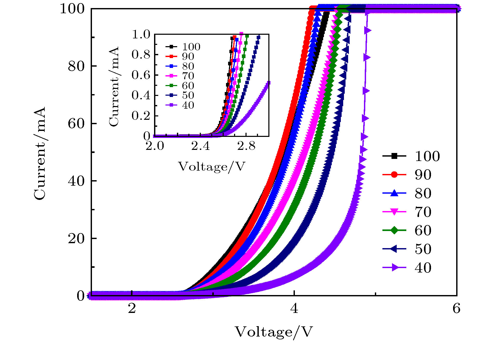
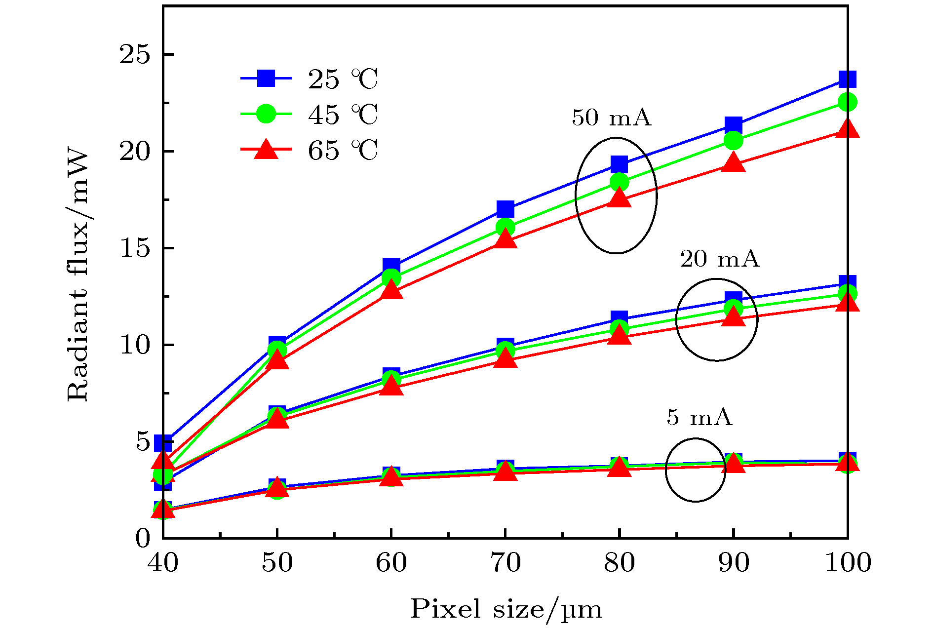
设计制备了不同大小的单颗微缩化发光二极管(Micro-LED)和Micro-LED阵列. 其中, 单颗Micro-LED尺寸为40—100 μm, 其电极结构为共N极, P极单独引出; 阵列像素数量为8 × 8, 被动驱动结构, 像素大小为60 μm. 器件制备过程中使用厚光刻胶作掩膜, 刻蚀N型GaN外延片至衬底, 形成隔离槽. 通过优化电极结构和厚度, 提高了P电极在隔离槽爬坡处的可靠性; 使用现场可编程门阵列(field-programmable gate array, FPGA)对Micro-LED被动阵列进行了驱动显示. 对于不同尺寸的单颗Micro-LED进行了电学、光学、热学等方面的测试分析. 结果表明: 随着尺寸的减小, Micro-LED所能承受的电流密度越大; Micro-LED与普通蓝光LED相比具有较大的k系数, 并且随着尺寸的减小, k系数的数值增大, 热稳定性不如传统蓝光LED. FPGA可以实现对Micro-LED被动阵列的良好驱动.Single micro-light emitting diodes(LEDs) with different sizes and array micro-LED are designed and prepared, where the sizes of the single micro-LEDs are in a range of 40−100 μm, their electrodes are all co-N electrodes, P electrode is drawn out alone; the number of array pixels is
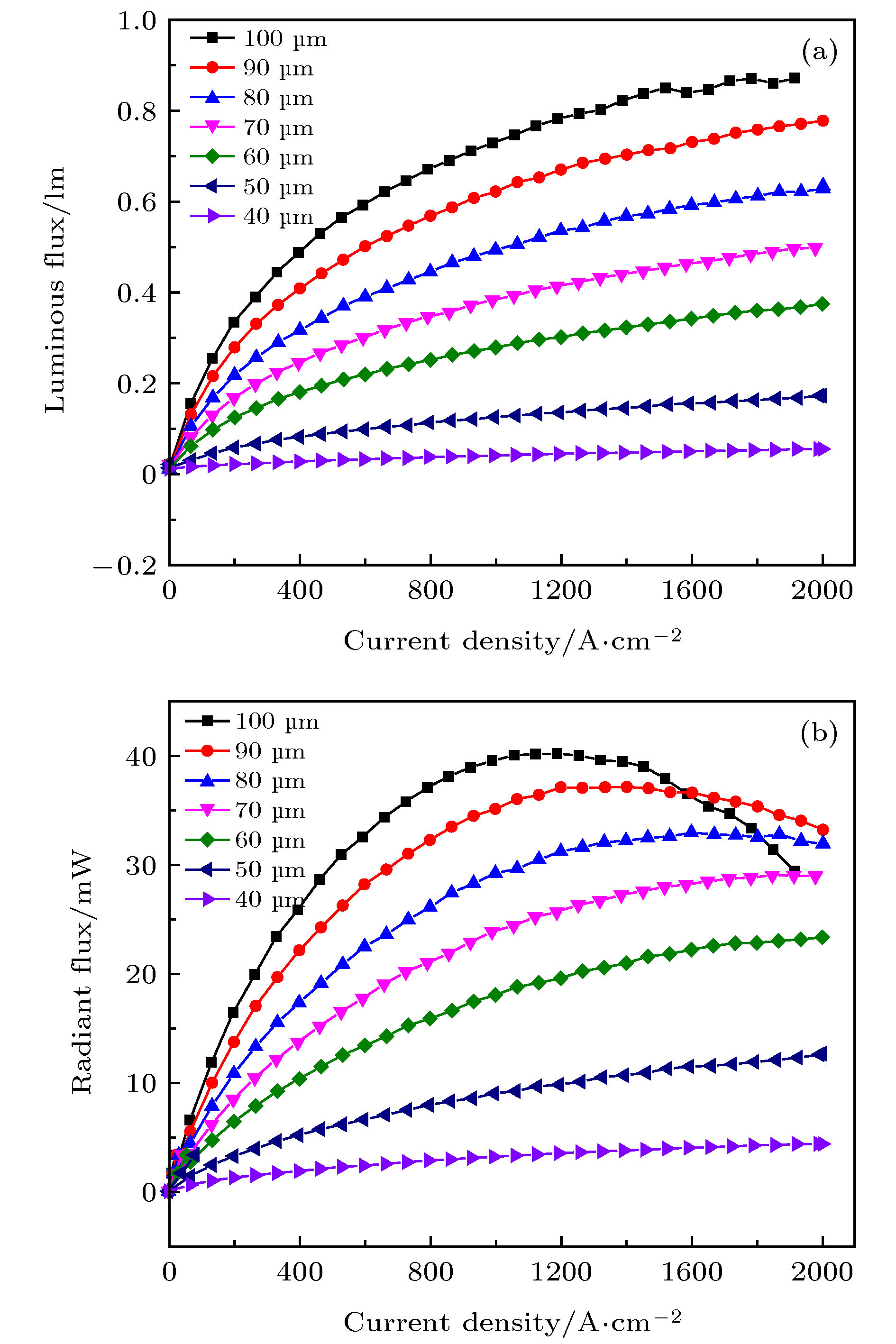
$ 8\times8 $ , which is a passively driving structure with a pixel size of 60 μm. In the process of device preparation, N electrode and P electrode are fabricated by the sputtering & stripping method. The electrode thickness is 2.4 μm. Thick photoresist 5120 is used as a mask, and N GaN is etched to the substrate by using the ICP dry etching to form an isolation trench. The PECVD technique is used to deposit an SiO2 insulating layer with a thickness of 10000 Å. By optimizing the electrode structure and thickness, the reliability of the P electrode at the slope of the isolation trench is improved, and the SiO2 insulating layer has good encapsulation; field programmable gate array (FPGA) is used to drive and display the micro-LED passive array. The single micro-LEDs of different sizes are tested and analyzed in the aspects of electrics, photics and thermotics and the results of which show that the current density corresponding to the peak radiation flux of 80 μm micro-LED is 1869.2 A/cm2, which is 57.1% higher than that of 100 μm micro-LED, indicating that the current density corresponding to the peak radiation flux of micro-LED increases as the size decreases; compared with the ordinary blue LED, the micro-LED has a large k factor, and with the size decreases, the value of the k factor increases, indicating that the micro-LED series resistance is larger, and the thermal stability is not so good as the traditional blue LED. Finally, the field programmable gate array (FPGA) can achieve a good drive for the micro-LED passive array. The driving principle is passive scanning driving, which is carried out in a row-by-row lighting mode. The FPGA clock is 50 MHz, and 320 ns is required for the circuit to scan all rows.-
Keywords:
- micro-light-emitting diode /
- size effect /
- k-factor /
- passive
[1] Gong Z, Jin S R, Chen Y J, Jonathan M, David M, Ian M W, Erdan G, Martin D D 2010 Appl. Phys. Lett. 97 013103
 Google Scholar
[2] Tian P F, Jonathan J D M, Gong Z, Benoit G, Ian M W, Erdan G, Chen Z Z, C, Zhang G Y, Martin D D 2012 Appl. Phys. Lett. 101 231110
 Google Scholar
[3] Olivier F, Daami A, Licitra C, Templier F 2017 Appl. Phys. Lett. 111 022104
 Google Scholar
[4] Zhan J L, Chen Z Z, Jiao Q Q J, Feng Y L, Li C C, Chen Y F, Chen Y Y, Jiao F, Kang X N, Li S F, Wang Q, Yu T J, Zhang G Y, Shen B 2018 Opt. Express 26 5265
 Google Scholar
[5] 邰建鹏, 郭伟玲 2019 照明工程学报 30 18
Tai J P, Guo W L 2019 China Illuminating Engineering Journal 30 18
[6] Jin S X, Li J, Li J Z, Lin J Y, Jiang H X 2000 Appl. Phys. Lett. 76 631
 Google Scholar
[7] Jeon C W, Kim K S, Dawson M D 2002 Phys. Stat. Sol. (a) 192 325
 Google Scholar
[8] Gong Z, Zhang H X, Gu E, Griffin C, Dawson M D, Poher V, Kennedy G, French P M W, Neil M A A 2007 IEEE Trans. Electron Dev. 54 2650
 Google Scholar
[9] Sun C W, Chao C H, Chen H Y, Chiu Y H, Yeh W Y, Wu M H, Yen H H, Liang C C 2012 SID Symposium Digest of Technical Papers 42 1042
[10] Li X B, Wu L, Liu Z J, Babar H, Chong W C, Lau K M, C. Patrick Y 2016 J. Lightwave Technol. 34 3449
 Google Scholar
[11] Liu Z J, Chong W C, Wong K M, Tam K H, Lau K M 2013 IEEE Photonics Technol. Lett. 25 2267
 Google Scholar
[12] Liu Z J, Chong W C, Wong K M, Lau K M 2013 J. Disp. Technol. 9 678
 Google Scholar
[13] Liu Z J, Chong W C, Wong K M, Lau K M 2015 J. Microelectronic Eng. 148 98
 Google Scholar
[14] Deng P, Zhang K, Liu Z J 2016 IEEE J. Electron Dev. Soc. 5 90
[15] Choi H W, Jeon C W, Dawson M D 2004 IEEE Electron Dev. Lett. 25 277
 Google Scholar
[16] Guo W L, Tai J P, Liu J P, Sun J 2019 J. Electronic Mater. 48 5195
 Google Scholar
[17] 李炳乾, 郑同场, 夏正浩 2009 物理学报 58 7189
 Google Scholar
Li B Q, Zheng T C, Xia Z H 2009 Acta Phys. Sin. 58 7189
 Google Scholar
[18] Cao X A, Teetsov J M, D’Evelyn M P, Merfeld D W, Yan C H 2004 Appl. Phys. Lett. 85 7
 Google Scholar
[19] Chong W C, Cho W K, Liu Z j, Wang C H, Lau K M 2014 IEEE Compound Semiconductor Integrated Circuit Symposium La Jolla, October 19−22, 2014 p978
[20] Deng P, Zhang K, Chao V S D, Mo W j, Lau K M, Liu Z J 2016 J. Disp. Technol. 7 742
[21] 李炳乾, 布良基, 甘雄文, 范广涵 2003 光子学报 32 1349
Li B Q, Bu L J, Gan X W, Fan G H 2003 Acta. Photon. Sin. 32 1349
-
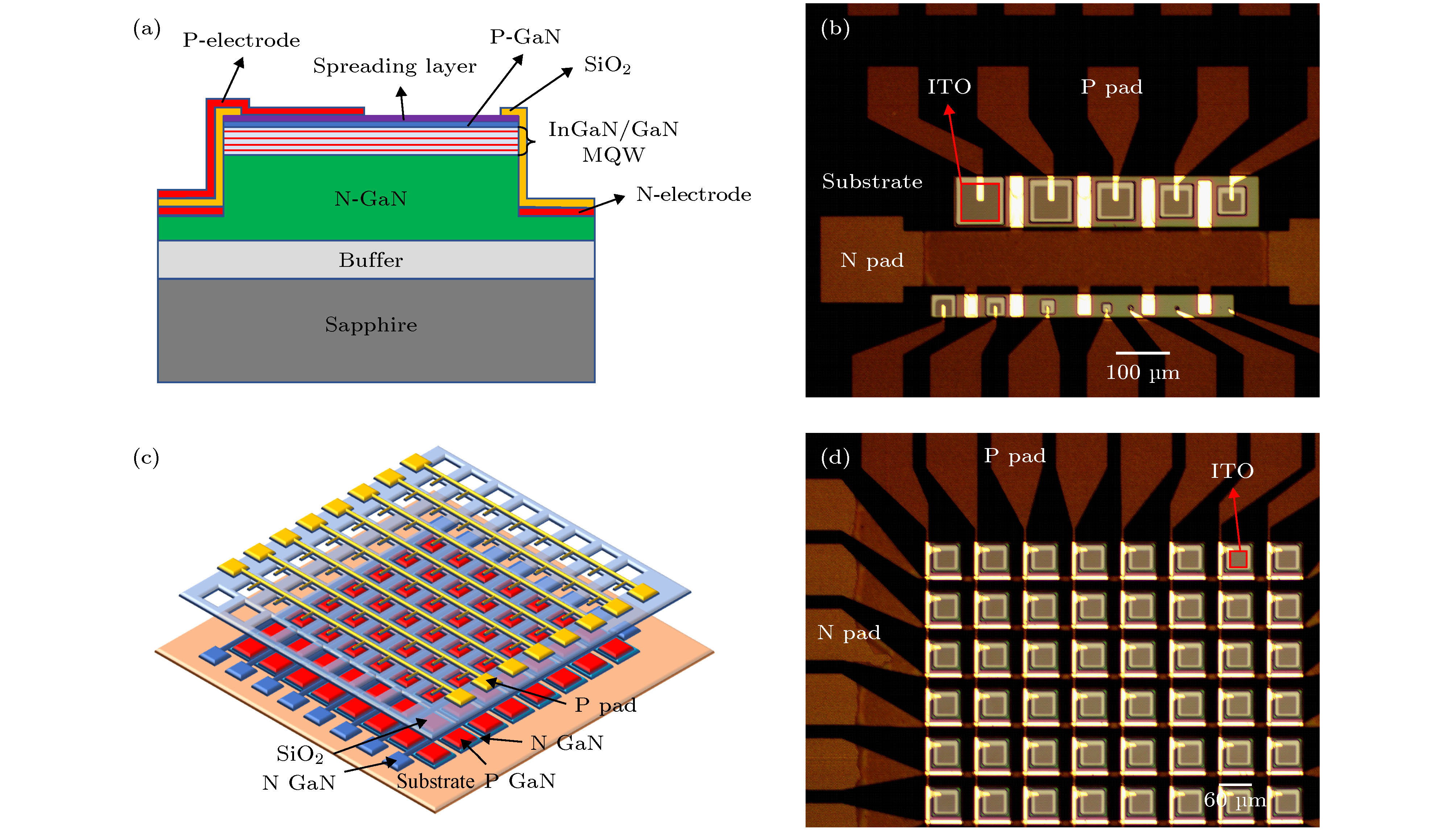
图 1 (a) Micro-LED结构示意图; (b) 尺寸为40—100 μm的Micro-LED光学显微图; (c) Micro-LED阵列3D结构图; (d) 阵列光学显微镜图
Fig. 1. (a) Schematic structure of single Micro-LED; (b) the optical micrograph of the Micro-LEDs with diameters from 40 μm to 100 μm; (c) 3D structure diagram of passive Micro-LED array; (d) optical micrograph.
图 4 不同测试电流下温度与电压的关系, 以及k系数与Micro-LED尺寸的关系 (a) 0.5 mA下温度与电压关系图; (b) 2 mA下温度与电压关系图; (c) 5 mA下温度与电压关系图; (d) 使用最小二乘法拟合图(a)—(c)得到的k系数与尺寸的关系曲线
Fig. 4. Temperature versus voltage curves with various test current, and Micro-LED size versus k coefficient: (a) Temperature versus voltage curves at 0.5 mA; (b) temperature versus voltage curves at 2 mA; (c) temperature versus voltage curves at 5 mA; (d) size and drive current versus k coefficient.
-
[1] Gong Z, Jin S R, Chen Y J, Jonathan M, David M, Ian M W, Erdan G, Martin D D 2010 Appl. Phys. Lett. 97 013103
 Google Scholar
[2] Tian P F, Jonathan J D M, Gong Z, Benoit G, Ian M W, Erdan G, Chen Z Z, C, Zhang G Y, Martin D D 2012 Appl. Phys. Lett. 101 231110
 Google Scholar
[3] Olivier F, Daami A, Licitra C, Templier F 2017 Appl. Phys. Lett. 111 022104
 Google Scholar
[4] Zhan J L, Chen Z Z, Jiao Q Q J, Feng Y L, Li C C, Chen Y F, Chen Y Y, Jiao F, Kang X N, Li S F, Wang Q, Yu T J, Zhang G Y, Shen B 2018 Opt. Express 26 5265
 Google Scholar
[5] 邰建鹏, 郭伟玲 2019 照明工程学报 30 18
Tai J P, Guo W L 2019 China Illuminating Engineering Journal 30 18
[6] Jin S X, Li J, Li J Z, Lin J Y, Jiang H X 2000 Appl. Phys. Lett. 76 631
 Google Scholar
[7] Jeon C W, Kim K S, Dawson M D 2002 Phys. Stat. Sol. (a) 192 325
 Google Scholar
[8] Gong Z, Zhang H X, Gu E, Griffin C, Dawson M D, Poher V, Kennedy G, French P M W, Neil M A A 2007 IEEE Trans. Electron Dev. 54 2650
 Google Scholar
[9] Sun C W, Chao C H, Chen H Y, Chiu Y H, Yeh W Y, Wu M H, Yen H H, Liang C C 2012 SID Symposium Digest of Technical Papers 42 1042
[10] Li X B, Wu L, Liu Z J, Babar H, Chong W C, Lau K M, C. Patrick Y 2016 J. Lightwave Technol. 34 3449
 Google Scholar
[11] Liu Z J, Chong W C, Wong K M, Tam K H, Lau K M 2013 IEEE Photonics Technol. Lett. 25 2267
 Google Scholar
[12] Liu Z J, Chong W C, Wong K M, Lau K M 2013 J. Disp. Technol. 9 678
 Google Scholar
[13] Liu Z J, Chong W C, Wong K M, Lau K M 2015 J. Microelectronic Eng. 148 98
 Google Scholar
[14] Deng P, Zhang K, Liu Z J 2016 IEEE J. Electron Dev. Soc. 5 90
[15] Choi H W, Jeon C W, Dawson M D 2004 IEEE Electron Dev. Lett. 25 277
 Google Scholar
[16] Guo W L, Tai J P, Liu J P, Sun J 2019 J. Electronic Mater. 48 5195
 Google Scholar
[17] 李炳乾, 郑同场, 夏正浩 2009 物理学报 58 7189
 Google Scholar
Li B Q, Zheng T C, Xia Z H 2009 Acta Phys. Sin. 58 7189
 Google Scholar
[18] Cao X A, Teetsov J M, D’Evelyn M P, Merfeld D W, Yan C H 2004 Appl. Phys. Lett. 85 7
 Google Scholar
[19] Chong W C, Cho W K, Liu Z j, Wang C H, Lau K M 2014 IEEE Compound Semiconductor Integrated Circuit Symposium La Jolla, October 19−22, 2014 p978
[20] Deng P, Zhang K, Chao V S D, Mo W j, Lau K M, Liu Z J 2016 J. Disp. Technol. 7 742
[21] 李炳乾, 布良基, 甘雄文, 范广涵 2003 光子学报 32 1349
Li B Q, Bu L J, Gan X W, Fan G H 2003 Acta. Photon. Sin. 32 1349
计量
- 文章访问数: 15183
- PDF下载量: 377
- 被引次数: 0


 下载:
下载:


