


-
外延生长铁电薄膜中基底失配应变能够调控微观铁电畴结构和宏观铁电性能. 本文选择了三种相结构(四方相、四方和菱方混合相、菱方相) PbZr(1–x)TixO3 (x = 0.8, 0.48, 0.2)铁电薄膜, 利用相场模拟研究了在不同基底失配应变(εsub)作用下, 三种成分铁电薄膜中微观畴结构的演化以及宏观极化-电场回线. 随着应变从–1.0%变化到1.0%, 三种相结构铁电薄膜的矫顽场、饱和极化值以及剩余极化值全都降低, 其中PbZr0.52Ti0.48O3薄膜的饱和极化值和剩余极化值比另外两种薄膜降低更快. 模拟结果表明拉应变能提高铁电薄膜储能效率, 其中准同型相界处应变提升储能效率最快. 本工作揭示了应变对PbZr(1–x)TixO3铁电薄膜中畴结构、电滞回线以及储能等方面的影响, 为铁电功能薄膜材料的实验设计提供了理论基础.Ferroelectric domain structures and ferroelectric properties in the hetero-epitaxially constrained ferroelectric thin films can be manipulated by substrate misfit strain. In this work, three kinds of phase structures of PbZr(1–x)TixO3 thin films, including tetragonal, tetragonal- rhombohedral-mixed and rhombohedral phases, are investigated. Firstly, the ferroelectric domain structures at different substrate misfit biaxial strains are obtained by the phase-field simulation. Then we calculate the polarization-electric field hysteresis loops at different misfit strains, and obtain the coercive field, saturation polarization, and remnant polarization. In the tetragonal PbZr(1–x)TixO3 (x = 0.8) thin film, compressive strain contributes to the formation of out-of-plane c1/c2 domain, and tensile strain favors in-plane a1/a2 domain formation. With the increase of compressive strain, the tetragonal phase and the rhombohedral phase coexist in PbZr(1–x)TixO3 (x = 0.48) film near the morphotropic phase boundary, while the tensile strain reduces the rhombohedral domain size. In the rhombohedral PbZr(1–x)TixO3 (x = 0.2) film, the rhombohedral domains are steady states under compressive strain and tensile strain. As the misfit strain changes from –1.0% to 1.0%, the value of the coercive field, saturation polarization and remnant polarization decrease. Among them, for tetragonal-rhombohedral mixed phase, the reductions of saturation field and remnant polarization are larger than for tetragonal phase and rhombohedral phase. The coercive field of mixed phase decreases rapidly under the compressive strain, but deceases slowly under the tensile strain. It is worth noting that the remnant polarization decreases faster than the saturation polarization in three components of ferroelectric thin film. Due to the electromechanical coupling, when x = 0.48 at the morphotropic phase boundary it is shown that the remnant polarization reduction is faster than those of the other two types of ferroelectric thin films, and the small coercive field is obtained in the case of large tensile strain. Therefore, tensile strain can effectively improve the energy storage efficiency in ferroelectric thin films, and the efficiency of x = 0.48 thin film increases significantly compared with that of x = 0.8 or 0.2 thin film. Both the ratio of rhombohedral/tetragonal phase and the domain size will play a significant role in ferroelectric performance. Therefore, our results contribute to the understanding of the electromechanical coupling mechanism of PbZr(1–x)TixO3, and provide guidance for the experimental design of ferroelectric functional thin film materials.
-
Keywords:
- phase-field simulation /
- misfit strain /
- ferroelectric domain structure /
- hysteresis loops
[1] Xu F, Trolier-McKinstry S, Ren W, Xu B, Xie Z L, Hemker K J 2001 J. Appl. Phys. 89 1336
 Google Scholar
[2] Kim D J, Maria J P, Kingon A I, Streiffer S K 2003 J. Appl. Phys. 93 5568
Google Scholar
[3] Karthik J, Martin L 2011 Phys. Rev. B 84 024102
Google Scholar
[4] Karthik J, Damodaran A R, Martin L W 2012 Phys. Rev. Lett. 108 167601
Google Scholar
[5] 赵晓英, 刘世建, 褚君浩, 戴宁, 胡古今 2008 物理学报 57 5968
Google Scholar
Zhao X Y, Liu S J, Chu J H, Dai N, Hu G J 2008 Acta Phys. Sin. 57 5968
Google Scholar
[6] Arimoto Y, Ishiwara H 2004 MRS Bull. 29 823
Google Scholar
[7] Ganapathi K L, Rath M, Rao M S R 2019 Semicond. Sci. Technol. 34 055016
Google Scholar
[8] Won S S, Seo H, Kawahara M, Glinsek S, Lee J, Kim Y, Jeong C K, Kingon A I, Kim S H 2019 Nano Energy 55 182
Google Scholar
[9] Hoshyarmanesh H, Ebrahimi N, Jafari A, Hoshyarmanesh P, Kim M, Park H H 2019 Sensors 19 13
Google Scholar
[10] Gupta R, Gupta V, Tomar M 2020 Mater. Sci. Semicond. Process. 105 104723
Google Scholar
[11] Rath M, Varadarajan E, Premkumar S, Shinde S, Natarajan V, Rao M S R 2019 Ferroelectrics 551 17
Google Scholar
[12] Yao Z H, Song Z, Hao H, Yu Z Y, Cao M H, Zhang S J, Lanagan M T, Liu H X 2017 Adv. Mater. 29 1601727
Google Scholar
[13] Pan H, Li F, Liu Y, Zhang Q, Wang M, Lan S, Zheng Y, Ma J, Gu L, Shen Y, Yu P, Zhang S, Chen L Q, Lin Y H, Nan C W 2019 Science 365 578
Google Scholar
[14] Wang J J, Su Y J, Wang B, Ouyang J, Ren Y, Chen L Q 2020 Nano Energy 72 104665
Google Scholar
[15] Li A D, Mak C L, Wong K H, Shao Q Y, Wang Y J, Wu D, Ming N B 2002 J. Cryst. Growth 235 307
Google Scholar
[16] Ehara Y, Shimizu T, Yasui S, Oikawa T, Shiraishi T, Tanaka H, Kanenko N, Maran R, Yamada T, Imai Y Sakata O, Valanoor N, Funakubo H 2019 Phys. Rev. B 100 104116
Google Scholar
[17] Izyumskaya N, Alivov Y I, Cho S J, Morkoç H, Lee H, Kang Y S 2007 Crit. Rev. Solid. State Mater. Sci. 32 111
Google Scholar
[18] Choi K J, Biegalski M, Li Y L, Sharan A, Schubert J, Uecker R, Reiche P, Chen Y B, Pan X Q, Gopalan V, Chen L Q, Schlom D G, Eom C B 2004 Science 306 1005
Google Scholar
[19] Noguchi Y, Maki H, Kitanaka Y, Matsuo H, Miyayama M 2018 Appl. Phys. Lett. 113 012903
Google Scholar
[20] Li Y L, Chen L Q 2006 Appl. Phys. Lett. 88 072905
Google Scholar
[21] Pertsev N A, Tagantsev A K, Setter N 2000 Phys. Rev. B 61 R825
Google Scholar
[22] Haeni J H, Irvin P, Chang W, Uecker R, Reiche P, Li Y L, Choudhury S, Tian W, Hawley M E, Craigo B, Tagantsev A K, Pan X Q, Streiffer S K, Chen L Q, Kirchoefer S W, Levy J, Schlom D G 2004 Nature 430 758
Google Scholar
[23] Zhang J X, Li Y L, Choudhury S, Chen L Q, Chu Y H, Zavaliche F, Cruz M P, Ramesh R, Jia Q X 2008 J. Appl. Phys. 103 094111
Google Scholar
[24] Ren W, Yang Y, Diéguez O, Íñiguez J, Choudhury N, Bellaiche L 2013 Phys. Rev. Lett. 110 187601
Google Scholar
[25] Zhang Y, Xue F, Chen Z H, Liu J M, Chen L Q 2020 Acta Mater. 183 110
Google Scholar
[26] Li Y L, Hu S Y, Liu Z K, Chen L Q 2002 Acta Mater. 50 395
Google Scholar
[27] Li Y L, Hu S Y, Chen L Q 2005 J. Appl. Phys. 97 034112
Google Scholar
[28] Yu Q, Li J, Zhu F, Li J 2014 J. Mater. Chem. C 2 5836
Google Scholar
[29] Lu X Y, Chen Z H, Cao Y, Tang Y L, Xu R J, Saremi S, Zhang Z, You L, Dong Y Q, Das S, Zhang H B, Zheng L M, Wu H P, Lv W M, Xie G Q, Liu X J, Li J Y, Chen L, Chen L Q, Cao W W, Martin L W 2019 Nat. Commun. 10 3951
Google Scholar
[30] Nguyen M D, Dekkers M, Houwman E, Steenwelle R, Wan X, Roelofs A, Schmitz-Kempen T, Rijnders G 2011 Appl. Phys. Lett. 99 252904
Google Scholar
[31] Xue F, Wang J J, Sheng G, Huang E, Cao Y, Huang H-H, Munroe P, Mahjoub R, Li Y, Valanoor N, Chen L 2013 Acta Mater. 61 2909
Google Scholar
[32] Lin F Y, Cheng X, Chen L Q, Sinnott S B 2018 J. Am. Ceram. Soc. 101 4783
Google Scholar
[33] Devonshire A F 1949 The London, Edinburgh, and Dublin Philosophical Magazine and Journal of Science 40 1040
Google Scholar
[34] Chen L Q 2008 J. Am. Ceram. Soc. 91 1835
Google Scholar
[35] Chen L Q 2002 Ann. Rev. Mater. Res. 32 113
Google Scholar
[36] Li Y L, Hu S Y, Liu Z K, Chen L Q 2001 Appl. Phys. Lett. 78 3878
Google Scholar
[37] Li Y L, Choudhury S, Liu Z K, Chen L Q 2003 Appl. Phys. Lett. 83 1608
Google Scholar
[38] Shu W L, Wang J, Zhang T Y 2012 J. Appl. Phys. 112 064108
Google Scholar
[39] Wang J J, Wang B, Chen L Q 2019 Ann. Rev. Mater. Res. 49 127
Google Scholar
[40] Li Y L, Chen L Q, Asayama G, Schlom D G, Zurbuchen M A, Streiffer S K 2004 J. Appl. Phys. 95 6332
Google Scholar
[41] Chen L Q, Shen J 1998 Comput. Phys. Commun. 108 147
Google Scholar
[42] Haun M J, Zhuang Z Q, Furman E, Jang S J, Cross L E 1989 Ferroelectrics 99 45
Google Scholar
[43] Hu H L, Chen L Q 1998 J. Am. Ceram. Soc. 81 492
[44] Damjanovic D 2005 J. Am. Ceram. Soc. 88 2663
Google Scholar
[45] Liu W F, Ren X B 2009 Phys. Rev. Lett. 103 257602
Google Scholar
[46] Li F, Lin D B, Chen Z B, Cheng Z X, Wang J L, Li C C, Xu Z, Huang Q W, Liao X Z, Chen L Q, Shrout T R, Zhang S J 2018 Nat. Mater. 17 349
Google Scholar
[47] Liao Z Y, Xue F, Sun W, Song D S, Zhang Q Q, Li J F, Chen L Q, Zhu J 2017 Phys. Rev. B 95 214101
Google Scholar
[48] Liu H, Chen J, Huang H B, Fan L L, Ren Y, Pan Z, Deng J X, Chen L Q, Xing X R 2018 Phys. Rev. Lett. 120 055501
Google Scholar
[49] Ma Z, Ma Y, Chen Z, Zheng F, Gao H, Liu H, Chen H 2018 Ceram. Int. 44 4338
Google Scholar
-

图 1 PZT铁电材料的晶体结构示意图 (a)立方顺电相结构; (b)四方铁电相结构; (c)正交铁电相结构; (d)菱方铁电相结构
Fig. 1. Schematic of PZT ferroelectric structure: (a) Paraelectric cubic phase; (b) ferroelectric tetragonal phase; (c) ferroelectric orthorhombic phase; (d) ferroelectric rhombohedral phase.
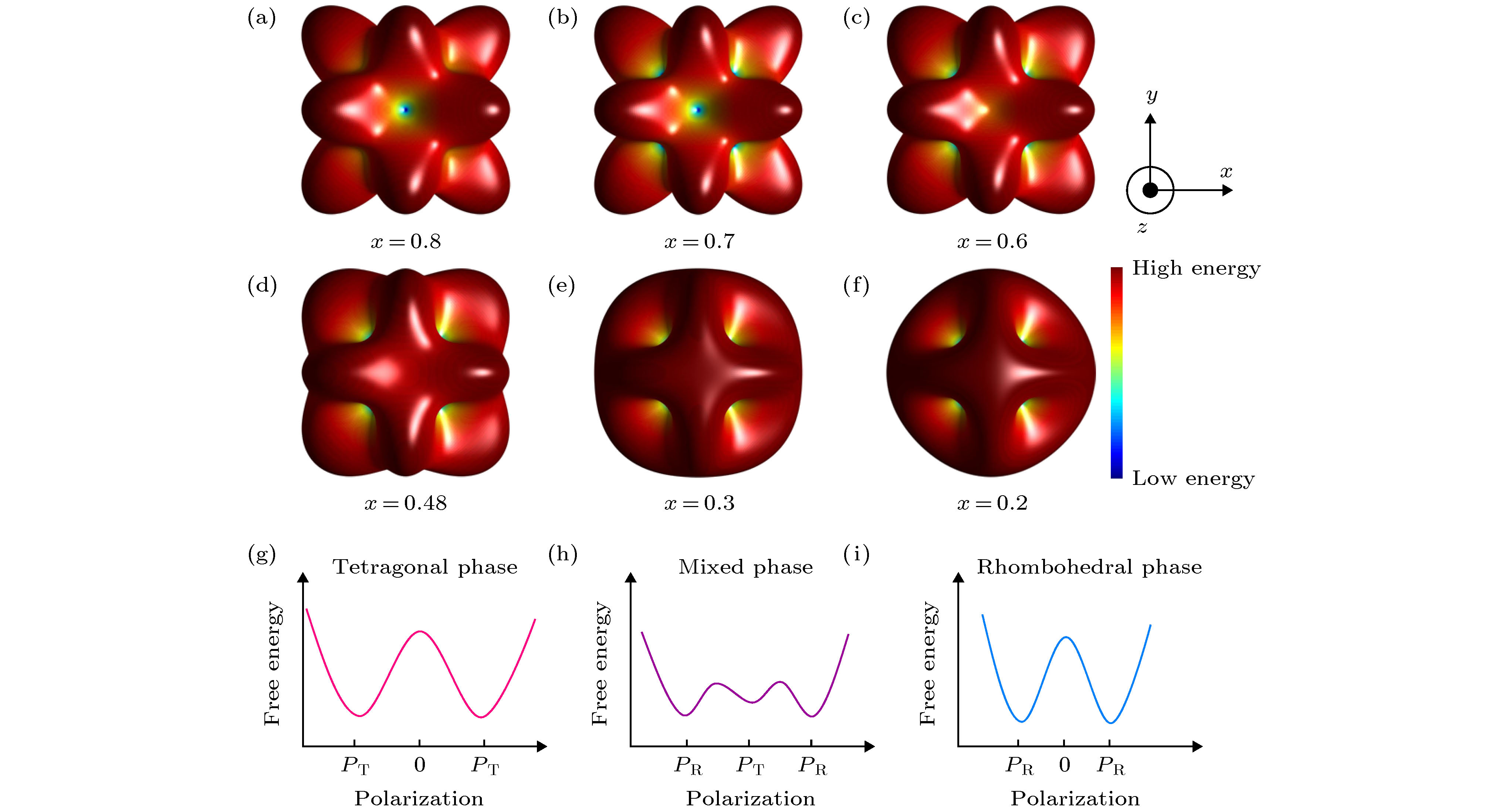
图 2 (a)−(f)室温下随Ti成分降低(x = 0.8—0.2) PZT的三维自由能曲面, 蓝色代表最小值, 红色代表最大值; (g)−(i) T相、R/T混合相及R相二维自由能双势阱示意图
Fig. 2. (a)−(f) Free energy surface of PZT with the decrease of Ti composition (x = 0.8–0.2) at room temperature. Blue and red color represents the minimum and maximum value respectively; (g)−(i) Schematic of double well potential of tetragonal phase (g), mixed phase (h) and rhombohedral phase (i).
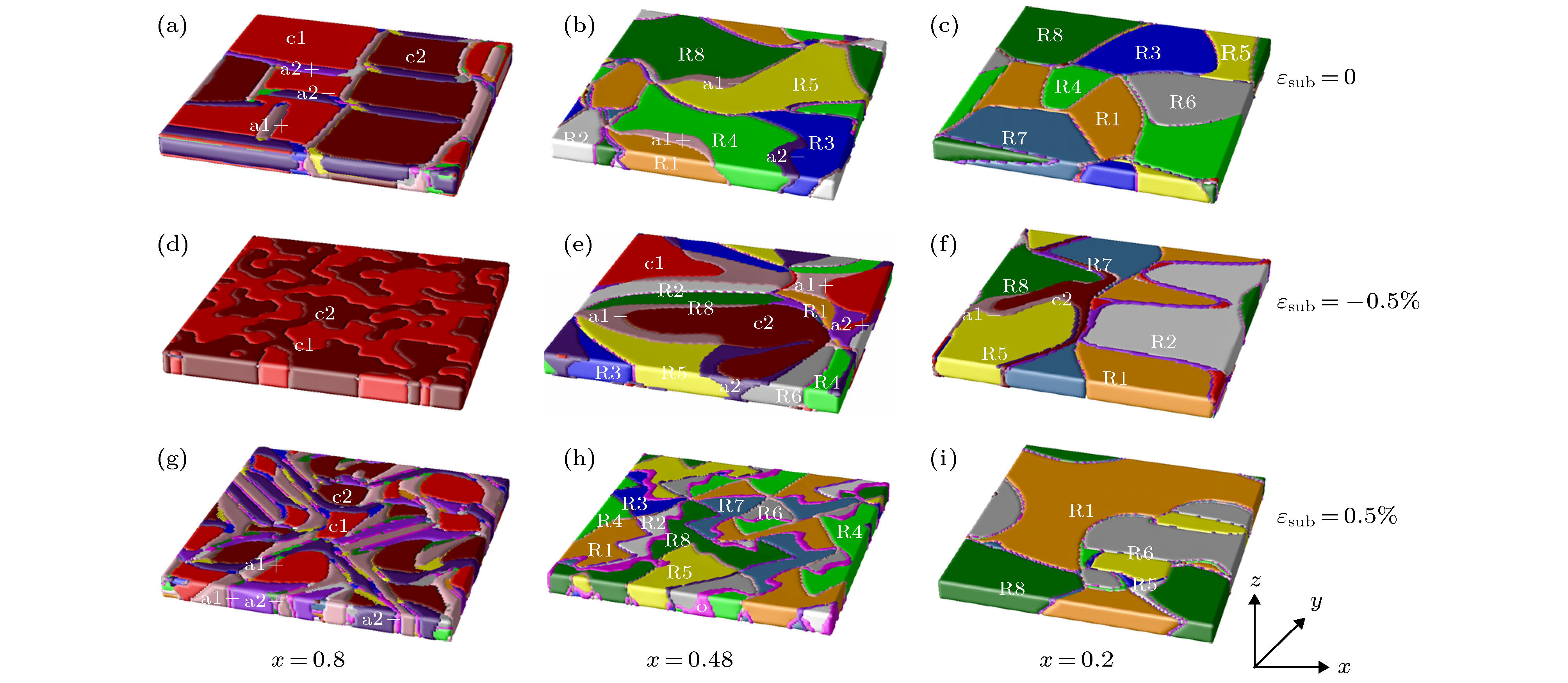
图 3 相场模拟PZT薄膜在不同基底失配应变下的畴结构 (a)—(c)分别对应于PZT (x = 0.8)薄膜εsub = 0, εsub = –0.5%, εsub = 0.5%; (d)—(f)分别对应于PZT (x = 0.48)薄膜εsub = 0, εsub = –0. 5%, εsub = 0.5%; (g)—(h)分别对应于PZT (x = 0.2)薄膜εsub = 0, εsub = –0.5%, εsub = 0.5%
Fig. 3. Domain structures of PZT (x = 0.8, x = 0.48, x = 0.2) thin film with different substrate biaxial misfit strain (εsub = 0, εsub = –0.5%, εsub = 0.5%): (a)−(c) Domain structures of PZT (x = 0.8) thin films at εsub = 0, εsub = –0.5%, εsub = 0.5%; (d)−(f) domain structures of PZT (x = 0.48) thin films at εsub = 0, εsub = –0.5%, εsub = 0.5%; (g)−(h) domain structures of PZT (x = 0.2) thin films at εsub = 0, εsub = –0.5%, εsub = 0.5%.

图 4 室温下PZT铁电薄膜四方相(x = 0.8), 混合相(x = 0.48)以及菱方相(x = 0.2)在不同的基底失配应变下(εsub = ± 0.1%, ± 0.5%, ± 1.0%)的电滞回线, 其中P *和E *表示归一化后的极化强度和电场强度值 (a)−(c)分别表示压应变下四方相、混合相和菱方相的电滞回线; (d)−(f)分别表示拉应变下四方相、混合相和菱方相的电滞回线
Fig. 4. Hysteresis loops of PZT thin films with three Ti components at different substrate biaxial misfit strains (εsub = ± 0.1%, ± 0.5%, ± 1.0%), and P * and E * are normalized polarization and electric field: (a)−(c) The case of compressive strains; (d)−(f) the case of tensile strains.
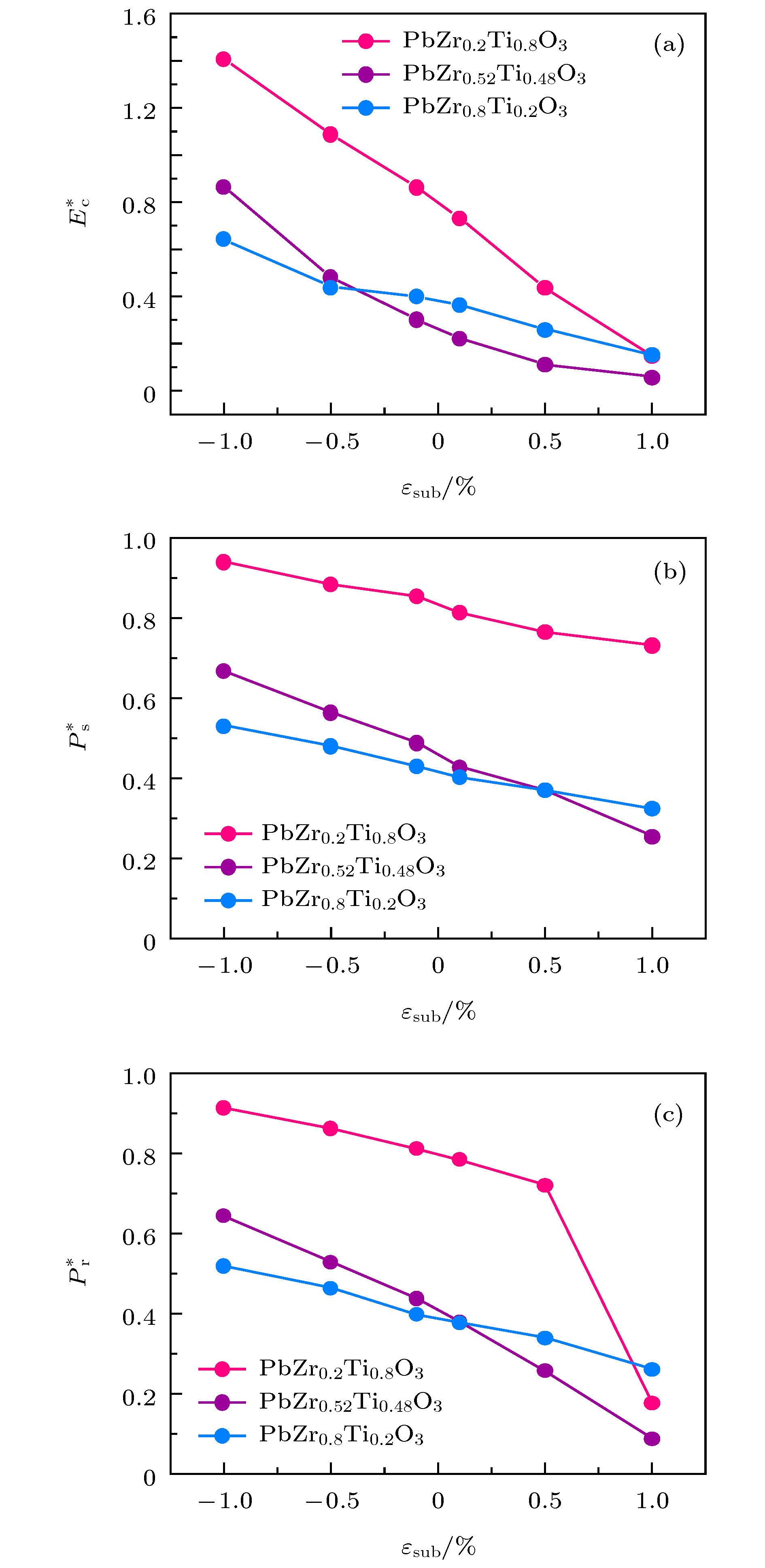
图 5 三种相PZT铁电薄膜的矫顽场、饱和极化和剩余极化值与基底应变的关系 (a) 矫顽场Ec*; (b) 饱和极化值Ps*; (c) 剩余极化值Pr*
Fig. 5. Normalized coercive field (Ec*), saturation polarization (Pr*), and remnant polarization (Ps*) as a function of substrate misfit strain (εsub), where three PZT ferroelectric thin films with x = 0.8, 0.48 and 0.2 Ti component are considered: (a) Coercive field vs. strain; (b) saturation polarization vs. strain; (c) remnant polarization vs. strain.
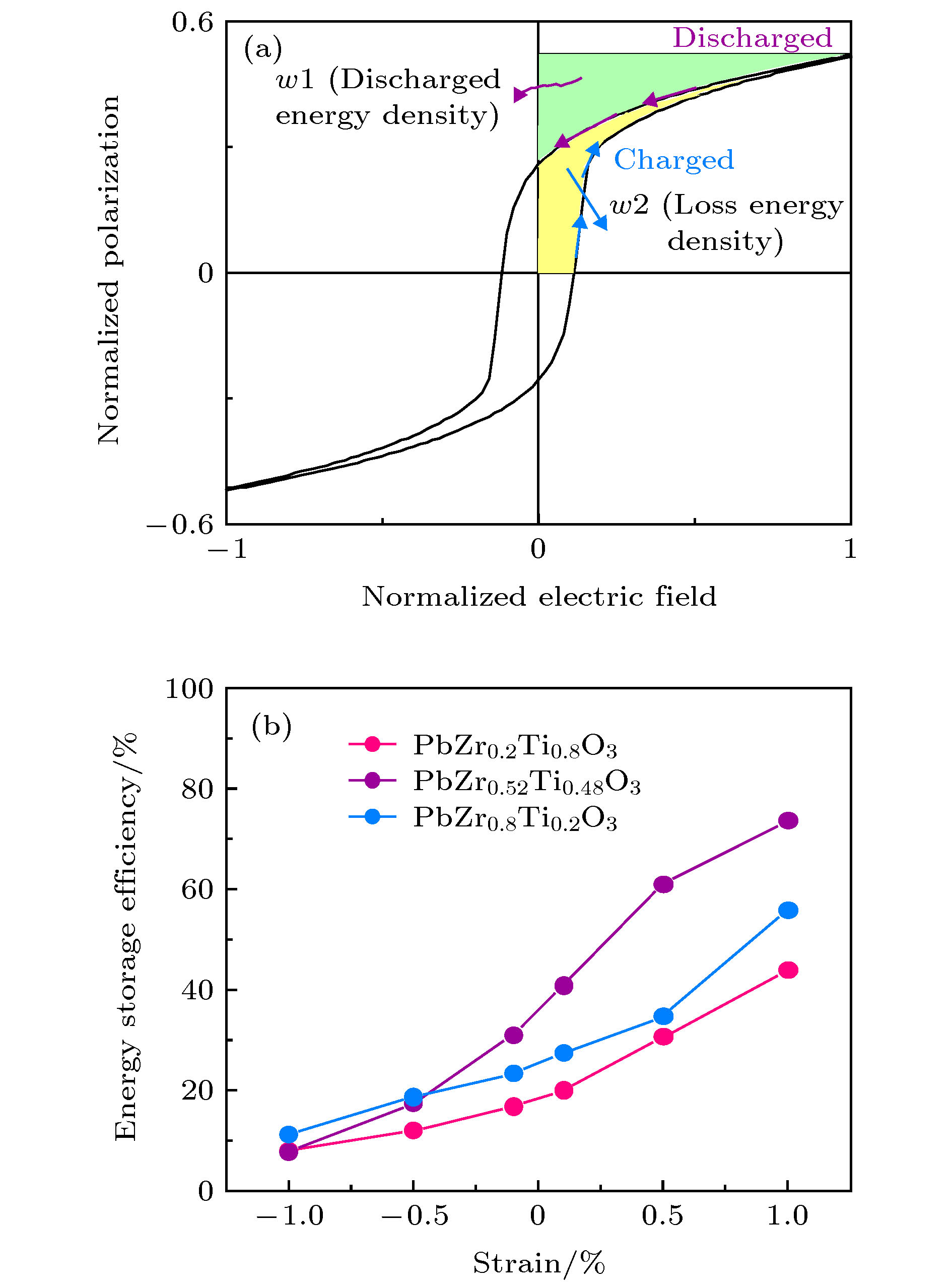
图 6 (a)电滞回线中充放电过程中储能示意图; (b) 三种PZT薄膜材料能量存储效率与基底应变之间的关系
Fig. 6. (a) Schematic of P-E loop used for energy storage; (b) the energy storage efficiency as a function of substrate misfit strain.
表 1 三种成分PZT铁电薄膜介电刚度系数和电致伸缩常数
Table 1. Corresponding material constants for the Landau free energy, the electrostrictive coefficients of three components PZT thin films.
Coefficients PbZr0.2Ti0.8O3 PbZr0.52Ti0.48O3 PbZr0.8Ti0.2O3 $ {a}_{1} $/C–2·m2·N 3.44 × 10⁵(T – 456.38) 1.45 × 10⁵(T – 387.06) 2.71 × 10⁵(T – 300.57) $ {a}_{11} $/C–4·m6·N –3.05 × 10⁷ 5.83 × 10⁷ 3.13 × 10⁸ $ {a}_{12} $/C–4·m6·N 6.32 × 10⁸ 1.82 × 10⁸ –3.45 × 10⁶ $ {a}_{111} $/C–6·m10·N 2.47 × 10⁸ 1.50 × 10⁸ 4.29 × 10⁸ $ {a}_{112} $/C–6·m10·N 9.68 × 10⁸ 6.88 × 10⁸ 1.81 × 10⁹ $ {a}_{123} $/C–6·m10·N –4.90 × 10⁹ –3.24 × 10⁹ –7.54 × 10⁹ $ {Q}_{11} $/C–2·m4 0.081 0.094 0.056 $ {Q}_{12} $/C–2·m4 –0.024 –0.044 –0.017 $ {Q}_{44} $/C–2·m4 0.032 0.040 0.026  下载: 导出CSV
表 2 三种PZT薄膜材料在不同应变下的储能效率值η
Table 2. Energy storage efficiency values of the PZT thin films under different strains.
Strain/% Energy storage efficienc η/% PbZr0.2Ti0.8O3 PbZr0.52Ti0.48O3 PbZr0.8Ti0.2O3 –1.0 8.0 7.8 11.2 –0.5 12.0 17.4 18.7 –0.1 16.8 31.0 23.4 0.1 20.0 40.6 27.4 0.5 30.7 61.0 34.7 1.0 43.9 73.6 55.8
下载: 导出CSV
-
[1] Xu F, Trolier-McKinstry S, Ren W, Xu B, Xie Z L, Hemker K J 2001 J. Appl. Phys. 89 1336
Google Scholar
[2] Kim D J, Maria J P, Kingon A I, Streiffer S K 2003 J. Appl. Phys. 93 5568
Google Scholar
[3] Karthik J, Martin L 2011 Phys. Rev. B 84 024102
Google Scholar
[4] Karthik J, Damodaran A R, Martin L W 2012 Phys. Rev. Lett. 108 167601
Google Scholar
[5] 赵晓英, 刘世建, 褚君浩, 戴宁, 胡古今 2008 物理学报 57 5968
Google Scholar
Zhao X Y, Liu S J, Chu J H, Dai N, Hu G J 2008 Acta Phys. Sin. 57 5968
Google Scholar
[6] Arimoto Y, Ishiwara H 2004 MRS Bull. 29 823
Google Scholar
[7] Ganapathi K L, Rath M, Rao M S R 2019 Semicond. Sci. Technol. 34 055016
Google Scholar
[8] Won S S, Seo H, Kawahara M, Glinsek S, Lee J, Kim Y, Jeong C K, Kingon A I, Kim S H 2019 Nano Energy 55 182
Google Scholar
[9] Hoshyarmanesh H, Ebrahimi N, Jafari A, Hoshyarmanesh P, Kim M, Park H H 2019 Sensors 19 13
Google Scholar
[10] Gupta R, Gupta V, Tomar M 2020 Mater. Sci. Semicond. Process. 105 104723
Google Scholar
[11] Rath M, Varadarajan E, Premkumar S, Shinde S, Natarajan V, Rao M S R 2019 Ferroelectrics 551 17
Google Scholar
[12] Yao Z H, Song Z, Hao H, Yu Z Y, Cao M H, Zhang S J, Lanagan M T, Liu H X 2017 Adv. Mater. 29 1601727
Google Scholar
[13] Pan H, Li F, Liu Y, Zhang Q, Wang M, Lan S, Zheng Y, Ma J, Gu L, Shen Y, Yu P, Zhang S, Chen L Q, Lin Y H, Nan C W 2019 Science 365 578
Google Scholar
[14] Wang J J, Su Y J, Wang B, Ouyang J, Ren Y, Chen L Q 2020 Nano Energy 72 104665
Google Scholar
[15] Li A D, Mak C L, Wong K H, Shao Q Y, Wang Y J, Wu D, Ming N B 2002 J. Cryst. Growth 235 307
Google Scholar
[16] Ehara Y, Shimizu T, Yasui S, Oikawa T, Shiraishi T, Tanaka H, Kanenko N, Maran R, Yamada T, Imai Y Sakata O, Valanoor N, Funakubo H 2019 Phys. Rev. B 100 104116
Google Scholar
[17] Izyumskaya N, Alivov Y I, Cho S J, Morkoç H, Lee H, Kang Y S 2007 Crit. Rev. Solid. State Mater. Sci. 32 111
Google Scholar
[18] Choi K J, Biegalski M, Li Y L, Sharan A, Schubert J, Uecker R, Reiche P, Chen Y B, Pan X Q, Gopalan V, Chen L Q, Schlom D G, Eom C B 2004 Science 306 1005
Google Scholar
[19] Noguchi Y, Maki H, Kitanaka Y, Matsuo H, Miyayama M 2018 Appl. Phys. Lett. 113 012903
Google Scholar
[20] Li Y L, Chen L Q 2006 Appl. Phys. Lett. 88 072905
Google Scholar
[21] Pertsev N A, Tagantsev A K, Setter N 2000 Phys. Rev. B 61 R825
Google Scholar
[22] Haeni J H, Irvin P, Chang W, Uecker R, Reiche P, Li Y L, Choudhury S, Tian W, Hawley M E, Craigo B, Tagantsev A K, Pan X Q, Streiffer S K, Chen L Q, Kirchoefer S W, Levy J, Schlom D G 2004 Nature 430 758
Google Scholar
[23] Zhang J X, Li Y L, Choudhury S, Chen L Q, Chu Y H, Zavaliche F, Cruz M P, Ramesh R, Jia Q X 2008 J. Appl. Phys. 103 094111
Google Scholar
[24] Ren W, Yang Y, Diéguez O, Íñiguez J, Choudhury N, Bellaiche L 2013 Phys. Rev. Lett. 110 187601
Google Scholar
[25] Zhang Y, Xue F, Chen Z H, Liu J M, Chen L Q 2020 Acta Mater. 183 110
Google Scholar
[26] Li Y L, Hu S Y, Liu Z K, Chen L Q 2002 Acta Mater. 50 395
Google Scholar
[27] Li Y L, Hu S Y, Chen L Q 2005 J. Appl. Phys. 97 034112
Google Scholar
[28] Yu Q, Li J, Zhu F, Li J 2014 J. Mater. Chem. C 2 5836
Google Scholar
[29] Lu X Y, Chen Z H, Cao Y, Tang Y L, Xu R J, Saremi S, Zhang Z, You L, Dong Y Q, Das S, Zhang H B, Zheng L M, Wu H P, Lv W M, Xie G Q, Liu X J, Li J Y, Chen L, Chen L Q, Cao W W, Martin L W 2019 Nat. Commun. 10 3951
Google Scholar
[30] Nguyen M D, Dekkers M, Houwman E, Steenwelle R, Wan X, Roelofs A, Schmitz-Kempen T, Rijnders G 2011 Appl. Phys. Lett. 99 252904
Google Scholar
[31] Xue F, Wang J J, Sheng G, Huang E, Cao Y, Huang H-H, Munroe P, Mahjoub R, Li Y, Valanoor N, Chen L 2013 Acta Mater. 61 2909
Google Scholar
[32] Lin F Y, Cheng X, Chen L Q, Sinnott S B 2018 J. Am. Ceram. Soc. 101 4783
Google Scholar
[33] Devonshire A F 1949 The London, Edinburgh, and Dublin Philosophical Magazine and Journal of Science 40 1040
Google Scholar
[34] Chen L Q 2008 J. Am. Ceram. Soc. 91 1835
Google Scholar
[35] Chen L Q 2002 Ann. Rev. Mater. Res. 32 113
Google Scholar
[36] Li Y L, Hu S Y, Liu Z K, Chen L Q 2001 Appl. Phys. Lett. 78 3878
Google Scholar
[37] Li Y L, Choudhury S, Liu Z K, Chen L Q 2003 Appl. Phys. Lett. 83 1608
Google Scholar
[38] Shu W L, Wang J, Zhang T Y 2012 J. Appl. Phys. 112 064108
Google Scholar
[39] Wang J J, Wang B, Chen L Q 2019 Ann. Rev. Mater. Res. 49 127
Google Scholar
[40] Li Y L, Chen L Q, Asayama G, Schlom D G, Zurbuchen M A, Streiffer S K 2004 J. Appl. Phys. 95 6332
Google Scholar
[41] Chen L Q, Shen J 1998 Comput. Phys. Commun. 108 147
Google Scholar
[42] Haun M J, Zhuang Z Q, Furman E, Jang S J, Cross L E 1989 Ferroelectrics 99 45
Google Scholar
[43] Hu H L, Chen L Q 1998 J. Am. Ceram. Soc. 81 492
[44] Damjanovic D 2005 J. Am. Ceram. Soc. 88 2663
Google Scholar
[45] Liu W F, Ren X B 2009 Phys. Rev. Lett. 103 257602
Google Scholar
[46] Li F, Lin D B, Chen Z B, Cheng Z X, Wang J L, Li C C, Xu Z, Huang Q W, Liao X Z, Chen L Q, Shrout T R, Zhang S J 2018 Nat. Mater. 17 349
Google Scholar
[47] Liao Z Y, Xue F, Sun W, Song D S, Zhang Q Q, Li J F, Chen L Q, Zhu J 2017 Phys. Rev. B 95 214101
Google Scholar
[48] Liu H, Chen J, Huang H B, Fan L L, Ren Y, Pan Z, Deng J X, Chen L Q, Xing X R 2018 Phys. Rev. Lett. 120 055501
Google Scholar
[49] Ma Z, Ma Y, Chen Z, Zheng F, Gao H, Liu H, Chen H 2018 Ceram. Int. 44 4338
Google Scholar

 下载:
下载:
计量
- 文章访问数: 17028
- PDF下载量: 606
- 被引次数: 0
