


-
基于第一性原理计算系统地研究了氮族、卤族和3d过渡金属元素(Ti, V, Cr, Mn, Fe, Co)替位掺杂对单层Janus过渡金属硫族化合物WSeTe电子结构的影响. 通过对能带结构、电荷转移以及磁性的分析, 发现氮(卤)族原子替位掺杂单层WSeTe会发生本征半导体-p (n)型半导体的转变, Ti, V原子替位掺杂单层WSeTe会发生半导体-金属的转变. 由于电荷转移以及氮族原子掺杂时价带顶的能带杂化现象, 卤族和氮族非金属元素掺杂时价带顶Γ点附近的Rashba自旋劈裂强度在同一主族随着掺杂原子原子序数的增大而增大. 3d过渡金属元素掺杂会产生能谷极化和磁性, 其中Cr, Mn原子替位掺杂会产生高于100 meV的能谷极化, 并且Cr, Mn, Fe元素掺杂在禁带中引入了电子自旋完全极化的杂质能级. 研究结果对系统地理解单层WSeTe掺杂模型的性质具有重要意义, 可以为基于单层WSeTe的电子器件设计提供理论参考.
-
关键词:
- 第一性原理计算 /
- Janus WSeTe /
- 替位掺杂
Based on the first principles calculations, the effects of substitutional doping of nitrogen, halogen and 3d transition metal elements on the electronic structure of monolayer Janus transition metal dichalcogenides WSeTe are studied in this paper, where the VASP software package is used based on density functional theory to perform calculations through using both the projector augmented wave method and the GGA-PBE functional method. A monolayer WSeTe hexagonal crystal system with 4 × 4 supercells is established, which contains 48 atoms. When VA (VIIA) element substitutes for monolayer WSeTe, one of the Se atoms is replaced with a nitrogen (halogen) atom; when the 3d transition metal element substitutes for monolayer WSeTe, one of the W atoms is replaced with a transition metal atom. Through the analysis of band structure, charge transfer and magnetism, it is found that VA (VIIA) nonmetallic elements doped monolayer WSeTe due to the introduction of the hole (electronic) doped, makes the Fermi level shift downward (upward), thus transforming into a p(n) type semiconductor. The Ti and V element substitutional doped monolayer WSeTe will present semiconductor-metal transformation. A doping for each of Cr, Co, Mn, Fe element doesn’t lead semiconductor material properties to change, but the each of Co, Mn, Fe element doped monolayer WSeTe can create a band gap of less than 20 meV. The VIIA (VA) non-metallic element and 3d transition metal element doped monolayer WSeTe will not have a huge influence on the original geometric structure of the material. Due to the charge transfer and doped atoms on the top of the valence band hybridization phenomenon, the Rashba spin splitting intensity near the Γ point of the top valence band increases with the increase of the atomic number of the doped atoms in the same main group when VIIA and VA non-metallic elements are doped. Moreover, the increase in atomic number and charge transfer have a greater influence on the strength of Rashba spin-orbit coupling than the change in electronegativity. The 3d transition metal element substitution doped single-layer WSeTe has obvious spin polarization phenomenon, which produces valley polarization near the Fermi level and introduces magnetism. In particular, since Cr-doped WSeTe retains the original semiconductor properties of WSeTe and has a large energy valley polarization, it may have a wide range of applications, such as in the field of spintronic devices. The monolayer WSeTe doped separately with Cr, Mn and Fe element produces an impurity band with fully polarized spin electrons in the band gap. The results are of great significance in systematically understanding the properties of monolayer WSeTe doping model and can provide theoretical reference for designing the monolayer WSeTe based electronic devices.-
Keywords:
- first principles calculation /
- Janus WSeTe /
- displacement doping
[1] Castro Neto A H, Guinea F, Peres N M R, Novoselov K S, Geim A K 2009 Rev. Mod. Phys. 81 109
 Google Scholar
[2] Song L, Ci L J, Lu H 2010 Nano Lett. 10 3209
Google Scholar
[3] Chhowalla M, Shin H S, Eda G, et al. 2013 Nat. Chem. 5 263
Google Scholar
[4] Li L K, Yu Y J, Ye G J 2014 Nat. Nanotechnol. 9 372
Google Scholar
[5] Ngai J H, Walker F J, Ahn C H 2014 Annu. Rev. Mater. Sci. 44 1
Google Scholar
[6] Shanmugam M, Jacobs-Gedrim R, Song E S 2014 Nanoscale 6 12682
Google Scholar
[7] 尹伟红, 韩勤, 杨晓红 2012 物理学报 61 248502
Google Scholar
Weihong Y, Qin H, Xiaohong Y 2012 Acta Phys. Sin. 61 248502
Google Scholar
[8] Withers F, Pozo-Zamudio O Del, Mishchenko A 2015 Nat. Mater. 14 301
Google Scholar
[9] Zhao Y, Li X, Xu M 2013 Opt. Express 21 3516
Google Scholar
[10] Tan C, Cao X, Wu X J 2017 Chem. Rev. 117 6225
Google Scholar
[11] Zhang X, Cheng H, Zhang H 2017 Adv. Mater. 29 1701704
Google Scholar
[12] Zhang X, Lai Z, Ma Q, Zhang H 2018 Chem. Soc. Rev. 47 3301
Google Scholar
[13] Cheng C, Sun J T, Chen X R, Fu H X, Meng S 2016 Nanoscale 8 17854
Google Scholar
[14] Cheng Y C, Zhu Z Y, Tahir M 2013 Europhys. Lett. 102 57001
Google Scholar
[15] Guo S D, Dong J 2018 Semicond. Sci. Technol. 33 085003
Google Scholar
[16] Shi Y, Li H, Li L J 2015 Chem. Soc. Rev. 44 2744
Google Scholar
[17] Li H, Lu G, Wang Y 2013 Small 9 1974
Google Scholar
[18] Balendhran S, Walia S, Nili H 2013 Adv. Funct. Mater. 23 3952
Google Scholar
[19] Feng Q, Mao N, Wu J 2015 ACS Nano 9 7450
Google Scholar
[20] Hu D, Xu G, Xing L 2017 Angew. Chem. Int. Ed. 56 3611
Google Scholar
[21] Ji Y, Yang M, Lin H 2018 J.Phys. Chem. C 122 3123
Google Scholar
[22] Meng M, Li T, Li S 2018 J. Phys. D: Appl. Phys. 51 105004
Google Scholar
[23] Wang M, Pang Y, Liu D Y 2018 Comput. Mater. Sci. 146 240
Google Scholar
[24] Guo S D 2018 Phys. Chem. Chem. Phys 20 7236
Google Scholar
[25] Er D, Ye H, Frey N C 2018 Nano Lett. 18 3943
Google Scholar
[26] Hor Y S, Richardella A, Roushan R, Xia Y, Checkelsky J G, Yazdani A 2009 Phys. Rev. B 79 195208
Google Scholar
[27] Wu M, Cao C, Jiang J Z 2010 Nanotechnology 21 505202
Google Scholar
[28] Yue Q, Chang S, Qin S, Li J 2013 Phys. Lett. A 377 1362
Google Scholar
[29] Ramasubramaniam A, Naveh D 2013 Phys. Rev. B 87 195201
Google Scholar
[30] Guan S S, Ke S S, Yu F F 2019 Appl. Surf. Sci. 496 143692
Google Scholar
[31] Kresse G, Kurthmuler J 1996 Comput. Mater. Sci. 6 15
Google Scholar
[32] Kresse G, Hafner J 1994 Phys. Rev. B 50 13181
Google Scholar
[33] Kresse G, Joubert D 1999 Phys. Rev. B 59 1758
Google Scholar
[34] Perdew J P, Burke K, Ernzerhof M 1996 Phys. Rev. Lett. 77 3865
Google Scholar
[35] Monkhorst H J, Pack J D 1976 Phys. Rev. B 13 5188
Google Scholar
[36] Zhao X W, Qiu B, Hu G C 2019 Appl. Surf. Sci. 490 172
Google Scholar
[37] Hu T, Jia F H, Zhao G D 2018 Phys. Rev. B 97 235404
Google Scholar
[38] He J J, Li S 2018 Comput. Mater. Sci. 152 151
Google Scholar
[39] Peng R, Ma Y D, Zhang S 2018 J. Phys. Chem. Lett. 9 3612
Google Scholar
-

图 1 (a) VA (VIIA)和(b) TM元素替位掺杂单层WSeTe的俯视图(上)和侧视图(下)及其布里渊区和高对称点示意图; (c) 4 × 4的单层WSeTe超胞的能带结构
Fig. 1. (a), (b) The top view (top) and the side view (bottom) of the substitutionally doped monolayer WSeTe of VA (VIIA) and TM elements, as well as the schematic diagram of Brillouin zone and high symmetry points; (c) the energy band structure of 4 × 4 monolayer WSeTe supercell.
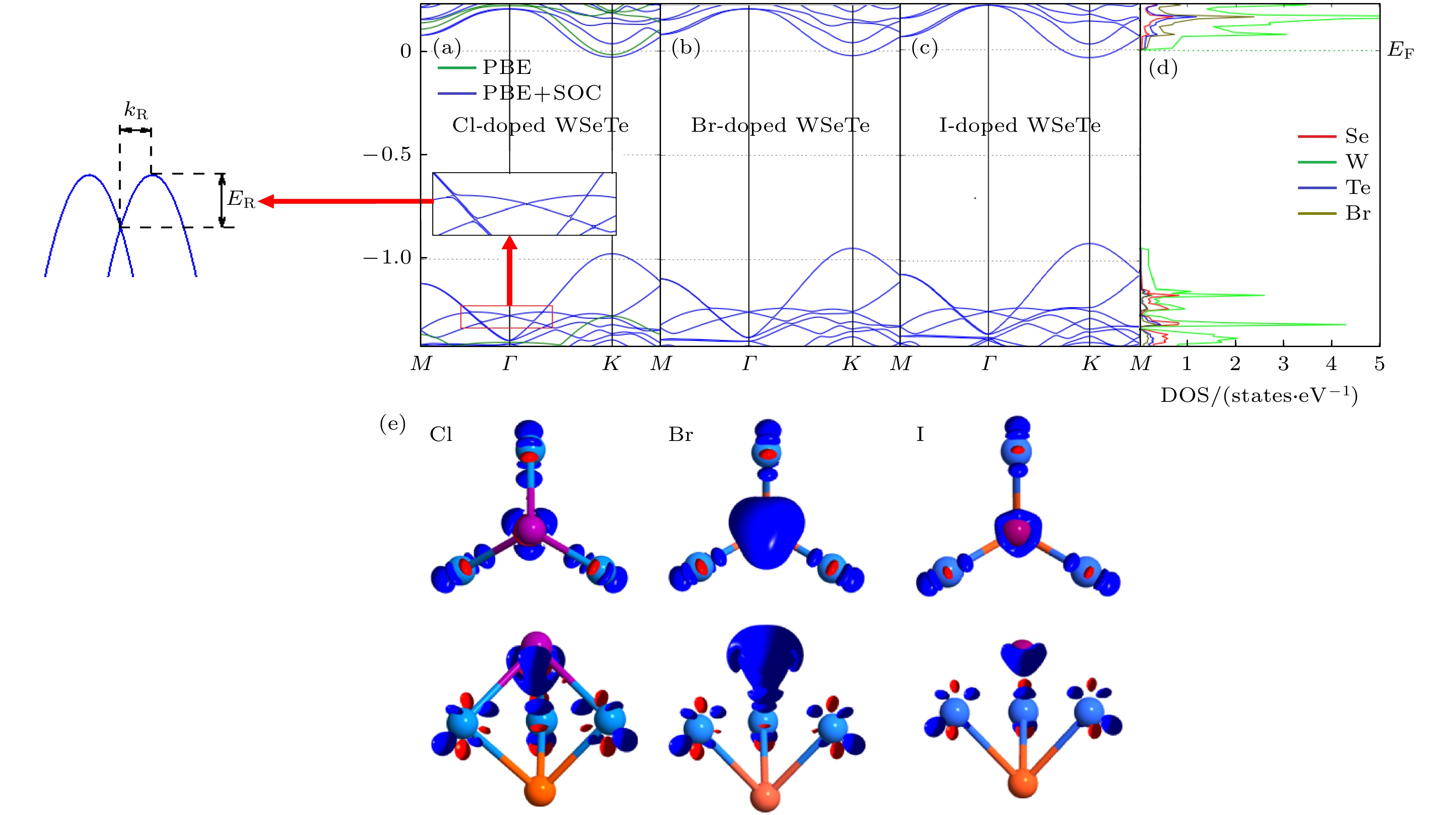
图 2 (a), (b), (c) Cl, Br, I原子掺杂单层WSeTe能带结构图; (d) Br原子掺杂单层WSeTe中单个原子的投影态密度图; (e) VIIA原子掺杂单层WSeTe的差分电荷密度的俯视图(上)和侧视图(下), 红色代表等值面0.01 a.u., 蓝色代表等值面–0.01 a.u.
Fig. 2. (a), (b), (c) The WSeTe band structure of Cl, Br and I atom doped, respectively; (d) the project density of state for each single atom in monolayer WSeTe doped by Br atom; (e) the top view (top) and side view (bottom) of the differential charge density of a monolayer WSeTe doped with VIIA atoms, red represents the isosurface 0.01 a.u. and blue represents the isosurface –0.01 a.u..
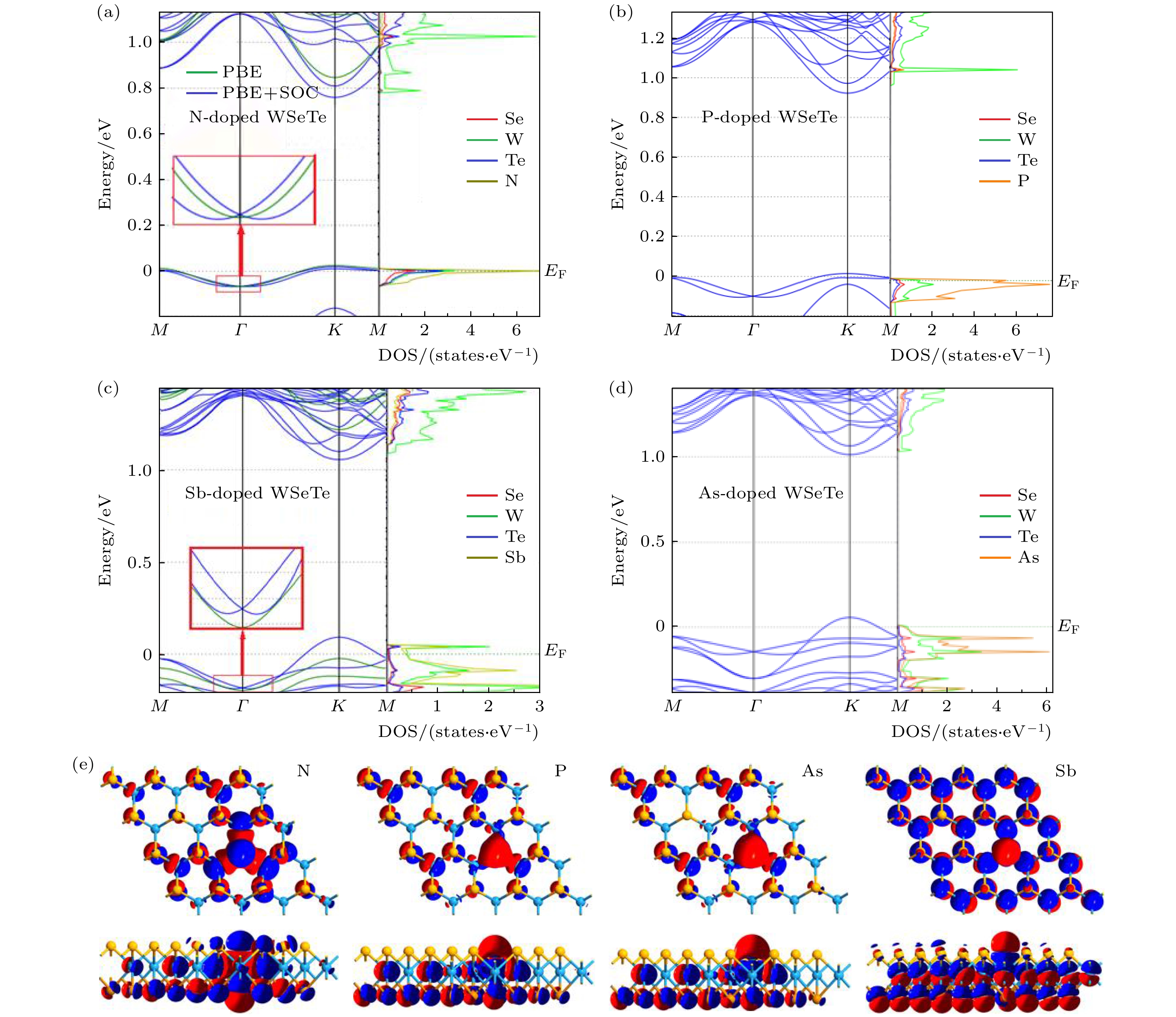
图 3 (a), (b), (c), (d) N, P, Sb, As掺杂单层WSeTe的能带结构图和单个原子的PDOS图; (e) VA原子掺杂单层WSeTe的差分电荷密度的俯视图(上)和侧视图(下), 红色代表等值面0.01 a.u., 蓝色代表等值面–0.01 a.u.
Fig. 3. (a), (b), (c), (d) The band structure diagram of N, P, Sb and As doped single-layer WSeTe and the PDOS diagram of a single atom, respectively; (e) the top view (top) and side view (bottom) of the differential charge density of a monolayer WSeTe doped with VA atoms, red represents the isosurface 0.01 a.u and blue represents the isosurface –0.01 a.u..

图 4 3d过渡金属元素掺杂单层WSeTe的能带图, 自旋在z轴方向的期望值
$ \left\langle {S}_{z} \right\rangle $ 的正负分别用红色和蓝色来表示,$ \left\langle {S}_{z} \right\rangle $ 绝对值的大小用点的大小来表示; 所有的能带经过平移使费米能级对齐, 同时费米能级固定在0 eV处Fig. 4. Band diagram of 3d transition metal elements doped monolayer WSeTe. The positive and negative values of the expected value
$ \left\langle {S}_{z} \right\rangle $ of the spin in the z-axis direction are represented by red and blue respectively, and the magnitude of the absolute value of$ \left\langle {S}_{z} \right\rangle $ is represented by the magnitude of the points. The spin projection along z-direction is depicted by the magnitude of the point. All the bands are shifted to align the Fermi level which is fixed at 0 eV.表 1 未掺杂体系的Se原子或VA (VIIA)掺杂原子和W原子之间的键长
$ {d}_{\mathrm{W}-\mathrm{D}} $ 、体系形成能$ {E}_{\mathrm{f}} $ 、掺杂原子得到的电荷数$ \Delta Q $ 以及Rashba常数$ \alpha $ Table 1. Bond length
$ {d}_{\mathrm{W}-\mathrm{D}} $ between VA (VIIA) doped atoms or Se atoms in an undoped system and W atoms, binding energy$ {E}_{\mathrm{f}} $ , the number of charges obtained by doping atoms$ \Delta Q $ and Rashba constant$ \alpha $ .Doped atom Se Cl Br I N P As Sb $ {d}_{\mathrm{W}-\mathrm{D}} $/Å 2.570 2.547 2.680 2.826 2.021 2.424 2.555 2.799 $ {E}_{\mathrm{f}} $/eV 0 0.16 0.35 0.46 –0.48 –0.2 0.25 0.65 $ \Delta Q $/e –0.47 –0.55 –0.46 –0.26 –1.23 –0.48 –0.24 –0.02 $ \alpha $/(eV·Å) 0.21 0.18 0.19 0.22 0.04 0.13 0.14 0.21  下载: 导出CSV
表 2 掺杂原子与Se (Te) 原子之间的键长
$ {d}_{\mathrm{S}\mathrm{e}-\mathrm{D}} $ ($ {d}_{\mathrm{T}\mathrm{e}-\mathrm{D}} $ )、结合能$ {E}_{\mathrm{f}} $ 、能谷极化的大小$ \Delta {E}_{K-K'} $ 及体系总的磁矩$ {M}_{\mathrm{t}\mathrm{o}\mathrm{t}\mathrm{a}\mathrm{l}} $ Table 2. Bond length
$ {d}_{\mathrm{S}\mathrm{e}-\mathrm{D}}\left({d}_{\mathrm{T}\mathrm{e}-\mathrm{D}}\right) $ between doped and Se (Te) atoms, binding energy$ {E}_{\mathrm{f}} $ , energy valley polarization$ \Delta {E}_{K-K'} $ and total magnetic moment$ { M}_{\mathrm{t}\mathrm{o}\mathrm{t}\mathrm{a}\mathrm{l}} $ Doped atom Ti Co Cr Mn Fe V $ {d}_{\mathrm{T}\mathrm{e}-\mathrm{D}} $/Å 2.778 2.587 2.724 2.733 2.768 2.733 $ {d}_{\mathrm{S}\mathrm{e}-\mathrm{D}} $/Å 2.577 2.462 2.547 2.551 2.588 2.558 $ {E}_{\mathrm{f}} $/eV –1.2 0.2 0.1 0.5 –1.7 –0.8 $ \Delta {E}_{K-K'} $/meV 26 2 108 105 34 73 $ {M}_{\mathrm{t}\mathrm{o}\mathrm{t}\mathrm{a}\mathrm{l}} $/$ {\mathrm{\mu }}_{\mathrm{B}} $ 1.46 2.99 0.01 1.02 2.01 0.94
下载: 导出CSV
-
[1] Castro Neto A H, Guinea F, Peres N M R, Novoselov K S, Geim A K 2009 Rev. Mod. Phys. 81 109
Google Scholar
[2] Song L, Ci L J, Lu H 2010 Nano Lett. 10 3209
Google Scholar
[3] Chhowalla M, Shin H S, Eda G, et al. 2013 Nat. Chem. 5 263
Google Scholar
[4] Li L K, Yu Y J, Ye G J 2014 Nat. Nanotechnol. 9 372
Google Scholar
[5] Ngai J H, Walker F J, Ahn C H 2014 Annu. Rev. Mater. Sci. 44 1
Google Scholar
[6] Shanmugam M, Jacobs-Gedrim R, Song E S 2014 Nanoscale 6 12682
Google Scholar
[7] 尹伟红, 韩勤, 杨晓红 2012 物理学报 61 248502
Google Scholar
Weihong Y, Qin H, Xiaohong Y 2012 Acta Phys. Sin. 61 248502
Google Scholar
[8] Withers F, Pozo-Zamudio O Del, Mishchenko A 2015 Nat. Mater. 14 301
Google Scholar
[9] Zhao Y, Li X, Xu M 2013 Opt. Express 21 3516
Google Scholar
[10] Tan C, Cao X, Wu X J 2017 Chem. Rev. 117 6225
Google Scholar
[11] Zhang X, Cheng H, Zhang H 2017 Adv. Mater. 29 1701704
Google Scholar
[12] Zhang X, Lai Z, Ma Q, Zhang H 2018 Chem. Soc. Rev. 47 3301
Google Scholar
[13] Cheng C, Sun J T, Chen X R, Fu H X, Meng S 2016 Nanoscale 8 17854
Google Scholar
[14] Cheng Y C, Zhu Z Y, Tahir M 2013 Europhys. Lett. 102 57001
Google Scholar
[15] Guo S D, Dong J 2018 Semicond. Sci. Technol. 33 085003
Google Scholar
[16] Shi Y, Li H, Li L J 2015 Chem. Soc. Rev. 44 2744
Google Scholar
[17] Li H, Lu G, Wang Y 2013 Small 9 1974
Google Scholar
[18] Balendhran S, Walia S, Nili H 2013 Adv. Funct. Mater. 23 3952
Google Scholar
[19] Feng Q, Mao N, Wu J 2015 ACS Nano 9 7450
Google Scholar
[20] Hu D, Xu G, Xing L 2017 Angew. Chem. Int. Ed. 56 3611
Google Scholar
[21] Ji Y, Yang M, Lin H 2018 J.Phys. Chem. C 122 3123
Google Scholar
[22] Meng M, Li T, Li S 2018 J. Phys. D: Appl. Phys. 51 105004
Google Scholar
[23] Wang M, Pang Y, Liu D Y 2018 Comput. Mater. Sci. 146 240
Google Scholar
[24] Guo S D 2018 Phys. Chem. Chem. Phys 20 7236
Google Scholar
[25] Er D, Ye H, Frey N C 2018 Nano Lett. 18 3943
Google Scholar
[26] Hor Y S, Richardella A, Roushan R, Xia Y, Checkelsky J G, Yazdani A 2009 Phys. Rev. B 79 195208
Google Scholar
[27] Wu M, Cao C, Jiang J Z 2010 Nanotechnology 21 505202
Google Scholar
[28] Yue Q, Chang S, Qin S, Li J 2013 Phys. Lett. A 377 1362
Google Scholar
[29] Ramasubramaniam A, Naveh D 2013 Phys. Rev. B 87 195201
Google Scholar
[30] Guan S S, Ke S S, Yu F F 2019 Appl. Surf. Sci. 496 143692
Google Scholar
[31] Kresse G, Kurthmuler J 1996 Comput. Mater. Sci. 6 15
Google Scholar
[32] Kresse G, Hafner J 1994 Phys. Rev. B 50 13181
Google Scholar
[33] Kresse G, Joubert D 1999 Phys. Rev. B 59 1758
Google Scholar
[34] Perdew J P, Burke K, Ernzerhof M 1996 Phys. Rev. Lett. 77 3865
Google Scholar
[35] Monkhorst H J, Pack J D 1976 Phys. Rev. B 13 5188
Google Scholar
[36] Zhao X W, Qiu B, Hu G C 2019 Appl. Surf. Sci. 490 172
Google Scholar
[37] Hu T, Jia F H, Zhao G D 2018 Phys. Rev. B 97 235404
Google Scholar
[38] He J J, Li S 2018 Comput. Mater. Sci. 152 151
Google Scholar
[39] Peng R, Ma Y D, Zhang S 2018 J. Phys. Chem. Lett. 9 3612
Google Scholar

 下载:
下载:


计量
- 文章访问数: 10652
- PDF下载量: 283
- 被引次数: 0
