


-
基于拜尔滤波片(bayer filter)彩色成像技术在集成度和分辨率都已经接近极限, 无滤波片(filter-free)的彩色成像单元得到广泛的关注和研究. 纳米线自身腔模式可以实现对不同能量的光空间分布, 通过对纳米线形貌调控实现色彩分辨探测. 本文使用有限元法构建了能依靠自身结构完成分光目的, 能够作为光探测器的锥形纳米线器件. 数值模拟结果显示, 能够根据器件的顶半径、底半径、长度和材料等相关参数调整器件涵盖的波长范围和分辨率等重要参数, 并具体分析了如何进行调控. 同时进一步分析了该结构在实际制备器件时以及不同角度入射光下的器件性能. 这些研究结果对于将锥形结构纳米线作为光探测器的实际应用有重要的参考意义.Filterless color discriminative imaging system is greatly demanded, with the pixel size shrinking to subwavelength. Nanowires have broad applications in photodetectors and have excellent ability to discriminate color by the cavity mode effect due to its well-controlled geometry. Here we use the finite element method to simulate a coned nanowire device which can split the light as well as serve as a photodetector array. The numerical simulation results show that the important parameters such as the wavelength range and resolution realized by the device can be modulated by the top radius, bottom radius, length, and material as well. And we also analyze how the surroundings and the incident angle affect the performance of the device. These results have important reference significance for the practical application of tapered nanowires as photodetectors.
-
Keywords:
- coned nanowire /
- photodetector /
- cavity mode
[1] Lim S J, Leem D S, Park K B, et al. 2015 Sci. Rep. 5 7708
 Google Scholar
[2] Kumar K, Duan H, Hegde R S, Koh S C, Wei J N, Yang J K 2012 Nat. Nanotechnol. 7 557
Google Scholar
[3] Yang Z, Albrow-Owen T, Cui H, et al. 2019 Science 365 1017
Google Scholar
[4] Zheng B J, Li L F, Wang J Z, Zhuge M H, Su X, Xu Y, Yang Q, Shi Y, Wang X M 2020 Adv. Opt. Mater. 8 2000191
Google Scholar
[5] Park H, Dan Y, Seo K, Yu Y J, Duane P K, Wober M, Crozier K B 2014 Nano Lett. 14 1804
Google Scholar
[6] Seo K, Wober M, Steinvurzel P, Schonbrun E, Dan Y, Ellenbogen T, Crozier K B 2011 Nano Lett. 11 1851
Google Scholar
[7] Park H, Crozier K B 2013 Sci. Rep. 3 2460
Google Scholar
[8] Cao L, Fan P, Barnard E S, Brown A M, Brongersma M L 2010 Nano Lett. 10 2649
Google Scholar
[9] Meng J J, Cadusch J J, Crozier K B 2020 Nano Lett. 20 320
Google Scholar
[10] Sherif S M, Elsayed M Y, Shahada L A, Swillam M A 2019 Appl. Phys. A 125 769
Google Scholar
[11] Kim S K, Day R W, Cahoon J F, Kempa T J, Song K D, Park H G, Lieber C M 2012 Nano Lett. 12 4971
Google Scholar
[12] Um H D, Solanki A, Jayaraman A, Gordon R G, Habbal F 2019 ACS Nano 13 11717
Google Scholar
[13] Yu L, Misra S, Wang J, Qian S, Foldyna M, Xu J, Shi Y, Johnson E, Cabarrocas P R 2014 Sci. Rep. 4 4357
[14] Lu J, Qian S, Yu Z, Misra S, Yu L, Xu J, Shi Y, Roca i Cabarrocas P, Chen K 2015 Opt. Express 23 A1288
Google Scholar
[15] Jiang Y, Zhai H, Cao W, Yang H, Liu H 2016 Electron. Mater. Lett. 12 841
Google Scholar
[16] Ming T, Schleusener A, Yermukhamed D, Dietzek B, Sivakov V 2019 Mater. Res. Express 6 2053
[17] Ling C, Guo T, Shan M, Zhao L, Sui H, Ma S, Xue Q 2019 J. Alloys Compd. 797 1224
Google Scholar
[18] Liang F X, Zhao X Y, Jiang J J, Hu J G, Xie W Q, Lü J, Zhang Z X, Wu D, Luo L B 2019 Small 15 e1903831
Google Scholar
[19] Yu Z, Qian S, Yu L, Misra S, Zhang P, Wang J, Shi Y, Xu L, Xu J, Chen K, Rocai Cabarrocas P 2015 Opt. Express 23 5388
Google Scholar
[20] Sumetsky M 2011 Opt. Lett. 36 145
Google Scholar
[21] Solanki A, Gentile P, Calvo V, Rosaz G, Salem B, Aimez V, Drouin D, Pauc N 2012 Nano Energy 1 714
Google Scholar
[22] Ajiki Y, Kan T, Yahiro M, Hamada A, Adachi J, Adachi C, Matsumoto K, Shimoyama I 2016 Appl. Phys. Lett. 108 151102
Google Scholar
[23] Dhyani V, Jakhar A, Wellington J J, Das S 2019 J. Phys. D: Appl. Phys. 52 425103
Google Scholar
[24] Bao J, Bawendi M G 2015 Nature 523 67
Google Scholar
[25] Kurokawa U, Choi B I, Chang C C 2011 IEEE Sens. J. 11 1556
Google Scholar
-
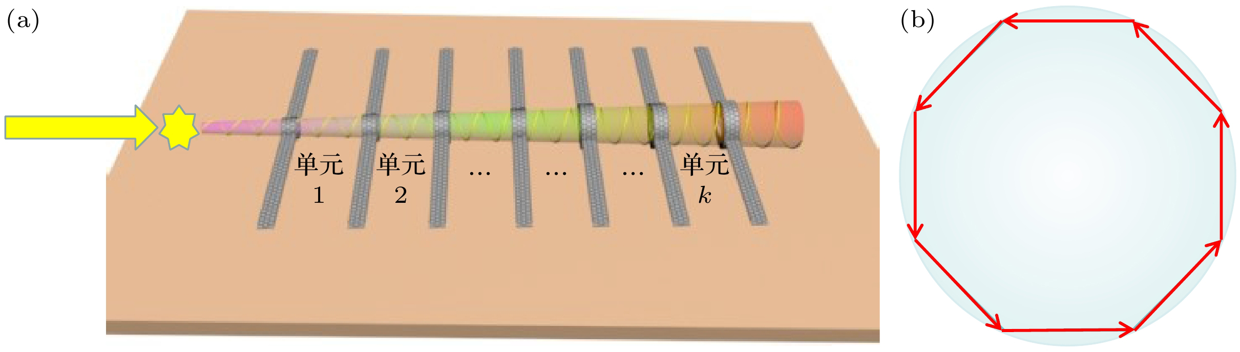
图 1 (a) 锥形纳米线器件结构示意图; (b) 回音壁模式原理示意图
Fig. 1. (a) Schematic diagram of the Si nano-cone device; (b) the whispering gallery mode.
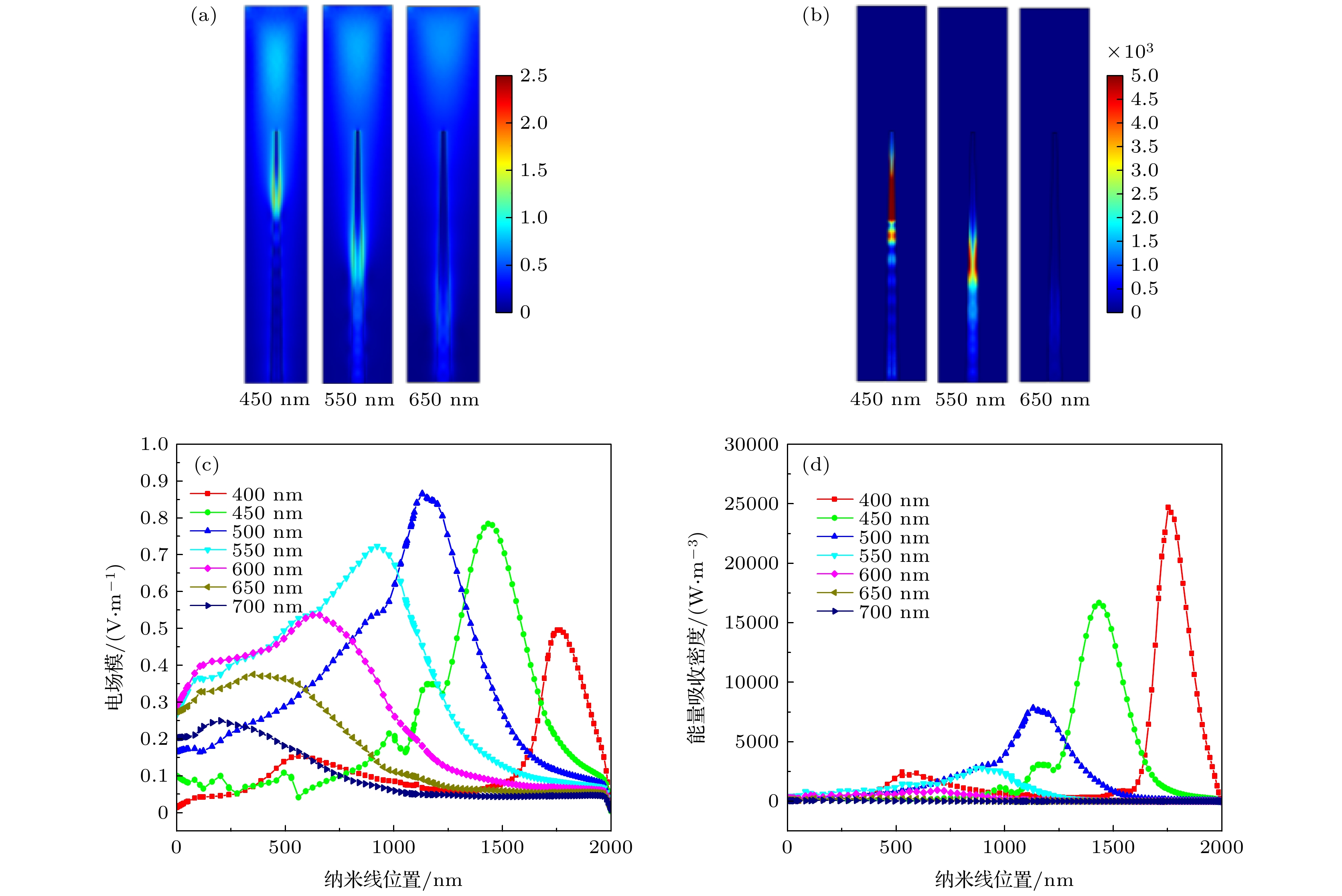
图 2 (a) 入射光为450 nm/550 nm/650 nm时的光场分布; (b) 入射光为450 nm/550 nm/650 nm时的吸收分布; (c) 不同入射光在器件轴线上的光场模分布曲线; (d) 不同入射光在器件轴线上的吸收密度分布曲线
Fig. 2. The simulation results of the light field distribution (a) and the absorption (b) with the wavelength of 450, 550 and 650 nm, respectively. The light field distribution (c) and absorption (d) of the typical incident wavelength along the axial of Si nano-cone.

图 3 (a) 入射光沿轴线入射时光场分布(左)及吸收分布(右); (b) 入射光5º入射时光场分布(左)及吸收分布(右); (c) 入射光10º入射时光场分布(左)及吸收分布(右); (d) 入射光30º入射时光场分布
Fig. 3. The simulation results of the light field distributions (left) and the absorption (right) with wavelength of 500 nm when the incident angle is (a) 0º, (b) 5º (c) 10º, and (d) 30º.
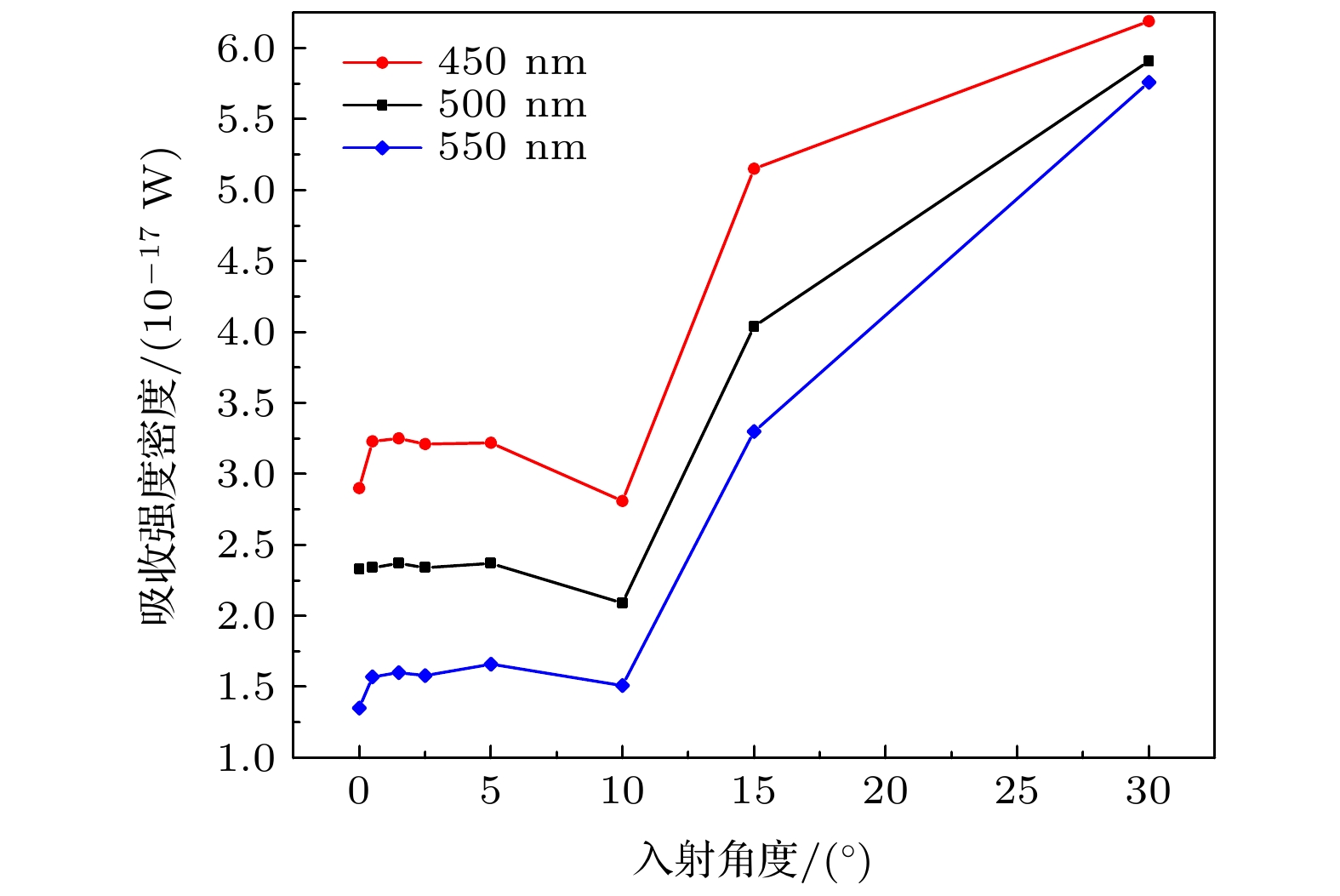
图 4 不同波长入射光在不同入射角度下锥形硅的能量吸收密度
Fig. 4. The energy absorption density of typical incident light with different incident angles.

图 5 入射光波长为420 nm时有石墨烯电极器件(a)和无石墨烯电极器件(b)光场分布对比; (c) 不同入射光在有石墨烯电极器件轴线上的光场分布曲线; (d) 不同入射光在无石墨烯电极器件轴线上的光场分布曲线
Fig. 5. (a) Comparisons of light field distribution between devices with (a) and without (b) graphene electrodes under incident light of with 420 nm. Light field distribution with typical incident light along the axis of nano-cone devices with (c) and without (d) graphene electrodes.
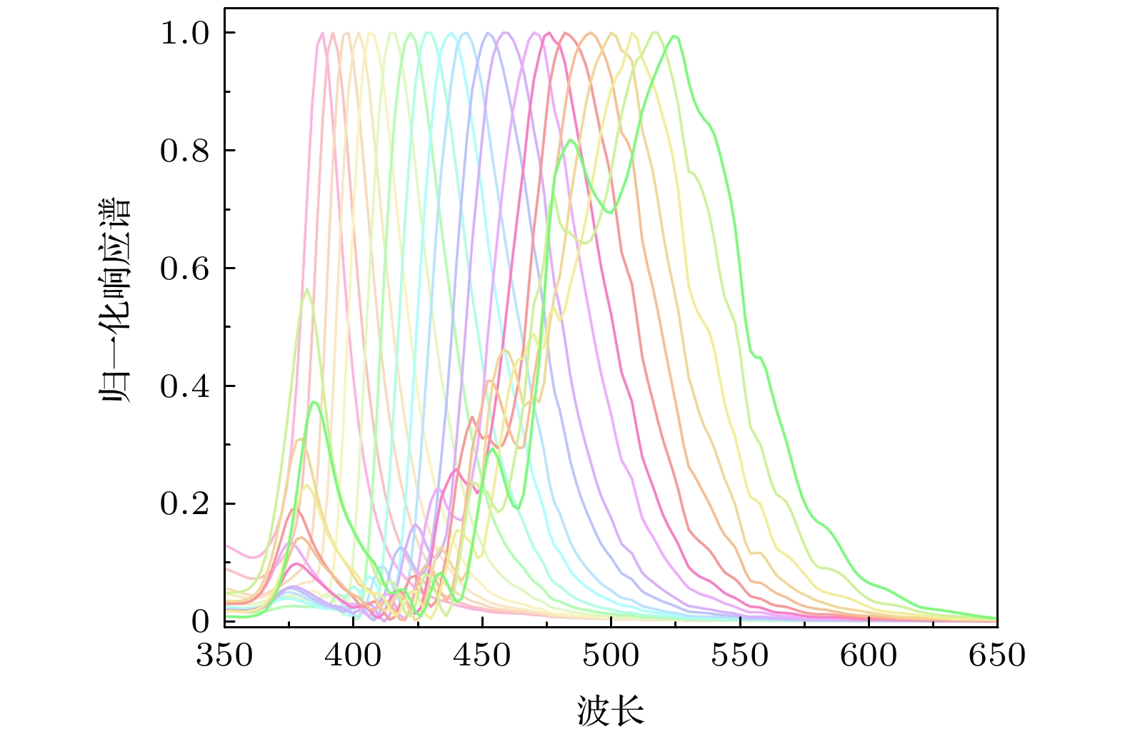
图 6 锥形纳米线器件归一化响应谱仿真结果
Fig. 6. The simulation results of normalized response spectrum of a nano-cone device.
表 1 在具有不同几何结构的器件中, 不同波长的入射光吸收最大值位置比较
Table 1. Comparisons of the max absorption position in different size devices with different geometry.
器件1/nm 器件2/nm 器件3/nm r1 = 20 r2 = 80 L = 2000 r1 = 20 r2 = 100 L = 2000 r1 = 20 r2 = 80 L = 2500 500 nm入射光吸收峰值直径/nm 92 94 90 550 nm入射光吸收峰值直径/nm 106 107 107 两峰值距离/nm 234 172 325  下载: 导出CSV
表 2 无衬底器件与有衬底器件对入射光能量吸收积分对比
Table 2. The total absorption of the nano-cone devices with or without substrate.
入射光波长550 nm 无衬底器件 衬底器件(入
射光偏振垂
直衬底)衬底器件(入
射光偏振平
行于衬底)与无衬底器件
比值 (光场)1 1.08 1.14 与无衬底器件
比值 (吸收)1 1.16 1.30
下载: 导出CSV
-
[1] Lim S J, Leem D S, Park K B, et al. 2015 Sci. Rep. 5 7708
Google Scholar
[2] Kumar K, Duan H, Hegde R S, Koh S C, Wei J N, Yang J K 2012 Nat. Nanotechnol. 7 557
Google Scholar
[3] Yang Z, Albrow-Owen T, Cui H, et al. 2019 Science 365 1017
Google Scholar
[4] Zheng B J, Li L F, Wang J Z, Zhuge M H, Su X, Xu Y, Yang Q, Shi Y, Wang X M 2020 Adv. Opt. Mater. 8 2000191
Google Scholar
[5] Park H, Dan Y, Seo K, Yu Y J, Duane P K, Wober M, Crozier K B 2014 Nano Lett. 14 1804
Google Scholar
[6] Seo K, Wober M, Steinvurzel P, Schonbrun E, Dan Y, Ellenbogen T, Crozier K B 2011 Nano Lett. 11 1851
Google Scholar
[7] Park H, Crozier K B 2013 Sci. Rep. 3 2460
Google Scholar
[8] Cao L, Fan P, Barnard E S, Brown A M, Brongersma M L 2010 Nano Lett. 10 2649
Google Scholar
[9] Meng J J, Cadusch J J, Crozier K B 2020 Nano Lett. 20 320
Google Scholar
[10] Sherif S M, Elsayed M Y, Shahada L A, Swillam M A 2019 Appl. Phys. A 125 769
Google Scholar
[11] Kim S K, Day R W, Cahoon J F, Kempa T J, Song K D, Park H G, Lieber C M 2012 Nano Lett. 12 4971
Google Scholar
[12] Um H D, Solanki A, Jayaraman A, Gordon R G, Habbal F 2019 ACS Nano 13 11717
Google Scholar
[13] Yu L, Misra S, Wang J, Qian S, Foldyna M, Xu J, Shi Y, Johnson E, Cabarrocas P R 2014 Sci. Rep. 4 4357
[14] Lu J, Qian S, Yu Z, Misra S, Yu L, Xu J, Shi Y, Roca i Cabarrocas P, Chen K 2015 Opt. Express 23 A1288
Google Scholar
[15] Jiang Y, Zhai H, Cao W, Yang H, Liu H 2016 Electron. Mater. Lett. 12 841
Google Scholar
[16] Ming T, Schleusener A, Yermukhamed D, Dietzek B, Sivakov V 2019 Mater. Res. Express 6 2053
[17] Ling C, Guo T, Shan M, Zhao L, Sui H, Ma S, Xue Q 2019 J. Alloys Compd. 797 1224
Google Scholar
[18] Liang F X, Zhao X Y, Jiang J J, Hu J G, Xie W Q, Lü J, Zhang Z X, Wu D, Luo L B 2019 Small 15 e1903831
Google Scholar
[19] Yu Z, Qian S, Yu L, Misra S, Zhang P, Wang J, Shi Y, Xu L, Xu J, Chen K, Rocai Cabarrocas P 2015 Opt. Express 23 5388
Google Scholar
[20] Sumetsky M 2011 Opt. Lett. 36 145
Google Scholar
[21] Solanki A, Gentile P, Calvo V, Rosaz G, Salem B, Aimez V, Drouin D, Pauc N 2012 Nano Energy 1 714
Google Scholar
[22] Ajiki Y, Kan T, Yahiro M, Hamada A, Adachi J, Adachi C, Matsumoto K, Shimoyama I 2016 Appl. Phys. Lett. 108 151102
Google Scholar
[23] Dhyani V, Jakhar A, Wellington J J, Das S 2019 J. Phys. D: Appl. Phys. 52 425103
Google Scholar
[24] Bao J, Bawendi M G 2015 Nature 523 67
Google Scholar
[25] Kurokawa U, Choi B I, Chang C C 2011 IEEE Sens. J. 11 1556
Google Scholar

 下载:
下载:
计量
- 文章访问数: 6701
- PDF下载量: 179
- 被引次数: 0
