


-
Z箍缩负载初始化电流通道的形成建立过程、电流密度分布模式及其演化特征对研究等离子体动力学发展、分析等离子体不稳定性模式、开展磁流体数值模拟工作等具有重要意义. 平面薄膜是研究这一问题中具有连续二维结构的理想构型. 基于理想无限长平板假设下的反场薄膜-回流柱负载模型, 通过理论对电感主导模式下的电流通道建立和演化过程、薄膜平面磁场分布特征和薄膜各部分受力特征进行了计算分析. 通过开展对称型与非对称型下的平面薄膜电爆炸实验, 以可见光分幅相机记录薄膜等离子体自辐射光分布为主要诊断手段开展了实验验证. 结果显示, 早期电流的建立与分布符合电感模型预期, 薄膜等离子体表现出电流密度边缘聚集和钳状型等离子体发光形态. 中后期图像显示发光强区会由薄膜边界向中心位置转移并导致峰状凸起型等离子体发光形态的演化, 表明电流分配受等离子体发展影响, 边界融蚀等离子体向心汇聚导致电流随之转移, 最终造成电流通道的快速切换.In the research of Z-pinch, the initial establishment of current in load, current density distribution mode and current evolution characteristics in different stages are of great significance in studying the development of plasma dynamics, analyzing plasma instability mode, and carrying out the MHD numerical simulation. Thin planar foil is an ideal configuration with continuous two-dimensional structure to study the problem. Based on an ideal model that consists of foil-backpost configuration under the assumption of infinite length in reverse exploding condition, the establishment, distribution and evolution of the current channel, magnetic field distribution characteristics and the force state of foil plasma by the inductive mode are calculated and analyzed theoretically. Relevant experiments are carried out on the QG-1 facility with about 1.4 MA peak current and 100 ns rise time to verify the calculated results. The self-emission graphs of exploding foils are recorded by visible-light frame cameras from side-on view and end-on view. Different load configurations are utilized including symmetric and asymmetric condition both assembled with two 20-μm-thick aluminum foils. The results show that the establishment of the initial current in foil (0–70 ns) accord with the expectation of the inductance model. The inductance feature determines the distribution of the current in this stage, which causes the current to aggregate in foil edges and then the edges will suffer much higher magnetic field and J × B force than the center. This results in the formation of a clamp plasma morphology. The later images (70–120 ns) show that the intense emission region will transfer from the foil edges to the center, which proves a transfer of current channel. So the magnetic field and J × B force in the foil center increase and a peak convex plasma morphology forms then. It shows that the current distribution will be affected by the plasma evolution process. The convergence process of ablated plasma with current finally leads to rapidly switch the current channel (in 60–80 ns).
[1] Ryutov D D, Derzon M S, Matzen M K 2000 Rev. Mod. Phys. 72 167
 Google Scholar
[2] Haines M G 2011 Plasma Phys. Controlled Fusion 53 093001
Google Scholar
[3] Chittenden J P, Lebedev S V, Bland S N, Ruiz-Camacho J, Beg F N, Haines M G 2001 Laser Part. Beams 19 323
Google Scholar
[4] Zhigalin A S, Rousskikh A G, Oreshkin V I, Chaikovsky S A, Ratakhin N A, Kuznetsov V V 2014 International Congress On Energy Fluxes And Radiation Effects Tomsk, Russia, September 21–26, 2014 012027
[5] Oreshkin V I 2008 Phys. Plasmas 15 092103
Google Scholar
[6] 丁宁, 张扬, 刘全, 肖德龙, 束小健, 宁成 2009 物理学报 58 1083
Google Scholar
Ding N, Zhang Y, Liu Q, Xiao D L, Shu X J, Ning C 2009 Acta Phys. Sin 58 1083
Google Scholar
[7] Lebedev S V, Beg F N, Bland S N, Chittenden J P, Dangor A E, Haines M G, Pikuz S A, Shelkovenko T A 2001 Laser Part. Beams 19 355
Google Scholar
[8] Jones B, Deeney C, McKenney J L, Garasi C J, Mehlhorn T A, Robinson A C, Wunsch S E, Bland S N, Lebedev S V, Chittenden J P, Bott S C, Ampleford D J, Palmer J B, Rapley J, Hall G N, Oliver B V 2005 Phys. Rev. Lett. 95 225001
Google Scholar
[9] Chittenden J P, Jennings C A 2008 Phys. Rev. Lett. 101 055005
Google Scholar
[10] Sinars D B, Slutz S A, Herrmann M C, McBride R D, Cuneo M E, Peterson K J, Vesey R A, Nakhleh C, Blue B E, Killebrew K, Schroen D, Tomlinson K, Edens A D, Lopez M R, Smith I C, Shores J, Bigman V, Bennett G R, Atherton B W, Savage M, Stygar W A, Leifeste G T, Porter J L 2010 Phys. Rev. Lett. 105 185001
Google Scholar
[11] Lebedev S V, Beg F N, Bland S N, Chittenden J P, Dangor A E, Haines M G, Kwek K H, Pikuz S A, Shelkovenko T A 2001 Phys. Plasmas 8 3734
Google Scholar
[12] Bland S N, Lebedev S V, Chittenden J P, Ampleford D J, Tang G 2004 Phys. Plasmas 11 4911
Google Scholar
[13] 刘永棠, 盛亮, 李阳, 张金海, 孟伦, 李豪卿, 袁媛, 孙铁平, 欧阳晓平 2021 物理学报 70 065203
Google Scholar
Liu Y T, Sheng L, Li Y, Zhang J H, Meng L, Li H Q, Yuan Y, Sun T P, Ouyang X P 2021 Acta Phys. Sin. 70 065203
Google Scholar
[14] Mikitchuk D, Cvejic M, Doron R, Kroupp E, Stollberg C, Maron Y, Velikovich A L, Ouart N D, Giulianli J L, Mehlhorn T A, Yu E P, Fruchtman A 2019 Phys. Rev. Lett. 122 045001
Google Scholar
[15] Lebedev S V, Beg F N, Bland S N, Chittenden J P, Dangor A E, Haines M G, Pikuz S A, Shelkovenko T A 2000 Phys. Rev. Lett. 85 98
Google Scholar
[16] 孟伦 2018 硕士学位论文(长沙: 国防科技大学)
Meng L 2018 M. S. Thesis (Changsha: National University of Defense Technology) (in Chinese)
[17] Clayson T, Lebedev S V, Suzuki-Vidal F, Burdiak G C, Halliday J W D, Hare J D, Ma J, Suttle L G, Tubman E R 2018 IEEE Trans. Plasma Sci. 46 3734
Google Scholar
[18] Burdiak G C, Lebedev S V, Bland S N, Clayson T, Hare J, Suttle L, Suzuki-Vidal F, Garcia D C, Chittenden J P, Bott-Suzuki S, Ciardi A, Frank A, Lane T S 2017 Phys. Plasmas 24 072713
Google Scholar
[19] Lebedev S V, Frank A, Ryutov D D 2019 Rev. Mod. Phys. 91 025002
Google Scholar
[20] Bott-Suzuki S C, Caballero Bendixsen L S, Cordaro S W, Blesener I C, Hoyt C L, Cahill A D, Kusse B R, Hammer D A, Gourdain P A, Seyler C E, Greenly J B, Chittenden J P, Niasse N, Lebedev S V, Ampleford D J 2015 Phys. Plasmas 22 052710
Google Scholar
[21] 盛亮 2007 博士学位论文 (北京: 清华大学)
Sheng L 2007 Ph. D. Dissertation (Beijing: Tsinghua University) (in Chinese)
[22] Davis J, Gondarenko N A, Velikovich A L 1997 Appl. Phys. Lett. 70 170
Google Scholar
[23] Strickler T S, Gilgenbach R M, Johnston M D, Yue Ying L 2003 IEEE Trans. Plasma Sci. 31 1384
Google Scholar
[24] 王亮平, 韩娟娟, 吴坚, 郭宁, 吴刚, 李岩, 邱爱慈 2010 物理学报 59 8685
Google Scholar
Wang L P, Han J J, Wu J, Guo N, Wu G, Li Y, Qiu A C 2010 Acta Phys. Sin 59 8685
Google Scholar
[25] Esaulov A A, Velikovich A L, Kantsyrev V L, Mehlhorn T A, Cuneo M E 2006 Phys. Plasmas 13 120701
Google Scholar
[26] Esaulov A A, Kantsyrev V L, Safronova A S, Velikovich A L, Cuneo M E, Jones B, Struve K W, Mehlhorn T A 2008 Phys. Plasmas 15 052703
Google Scholar
[27] Velikovich A L, Sokolov I V, Esaulov A A 2002 Phys. Plasmas 9 1366
Google Scholar
[28] Hu Min, Kusse B R 2005 Phys. Plasmas 12 102701
Google Scholar
-

图 1 诊断系统光路示意图与负载装配结构图
Fig. 1. Optical path of the diagnostic system and assembled load diagram.

图 2 不同结构负载侧向激光阴影图示 (a) 对称型薄膜负载; (b) 非对称型薄膜负载
Fig. 2. Side-on laser shadow graphs of the experimental load with different structures: (a) Symmetric load; (b) asymmetric load.
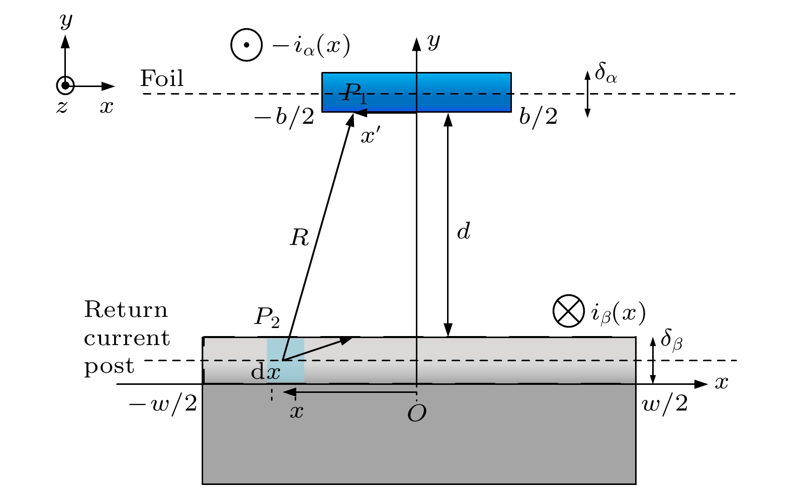
图 3 单侧薄膜-回流柱负载模型轴向图示. 电流方向为从薄膜底部流入顶部流出, 然后向下流进回流柱. w为回流柱宽度, b为薄膜宽度, d为两者间距. x为微元横坐标, x′为矢势研究点横坐标, R为微元与研究点间距, iα为薄膜面电流密度大小, iβ为回流柱边界处面电流密度大小. δα为薄膜载流厚度, δβ 为回流柱边界趋肤深度
Fig. 3. Diagram of 2-D foil-backpost geometry of axial direction view. Current flows into the foil from the bottom and flows out of the foil down to the return current post. w is the width of the return current post, b is the width of the foil, d is the distance between foil and post. x is the coordinate of the element, x' is the coordinate of the studied point, R is the distance between the element and studied point, iα is the surface current density of the foil and iβ is that of the backpost. δα is the flowing depth of current in the foil and δβ is that of the post boundary.

图 4 无限长有限宽理想平板构型在电流均匀分布假设下, 平板所在平面总磁感应强度分布. 载流厚度δ为20 μm, 平板范围为–5—5 mm, 平均电流密度大小为ja. 蓝色曲线为平板模型理论公式计算结果, 红色点集为单排电流柱微元近似薄膜微元下的数值计算结果
Fig. 4. Assuming equal distribution of current, calculated numerical B-field on slab by single-row model comparing to the theoretical value. Current depth is 20 μm, slab region is from –5 to 5 mm and ja is the average current density. Blue line is the numerical result and red plots are the theoretical result.
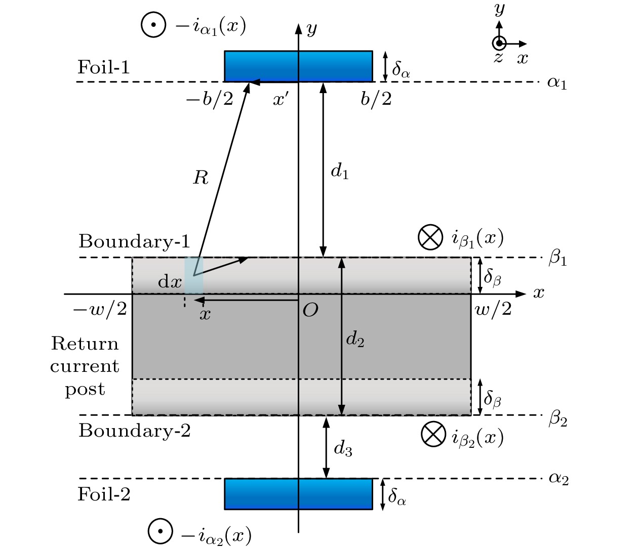
图 5 双侧薄膜结构负载模型轴向示意图. d1为远端薄膜距回流柱边界距离, d3为近端薄膜距回流柱边界距离, d2为回流柱宽度. i 为面电流密度, δ 为载流厚度, 其下标α1, β1, α2, β2分别对应薄膜1、回流柱界面1、薄膜2和回流柱界面2
Fig. 5. Diagram of the load structure with double foils from axial view. d1 is the distance between the further side foil α1 and post boundary β1, d3 is the distance between the other side foil α2 and post boundary β2, d2 is the width of the return current post, i is the surface current density, δ is the current depth where subscripts α1, β1, α2, β2 correspond to foil-1, post boundary-1, foil-2, post boundary-2, respectively
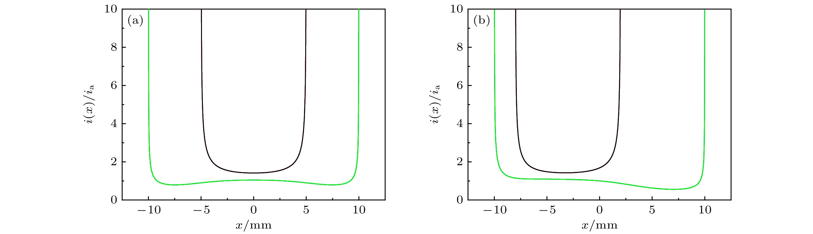
图 6 双侧对称型结构负载电流密度分布(d1 = 5 mm, d2 = 10 mm, d3 = 5 mm, 对应于图5结构. 其中红色(与黑色重合)对应薄膜α1, α2, 蓝色(与绿色重合)对应回流柱界面β1, β2) (a) 无偏置; (b) 薄膜左偏置0.3 mm
Fig. 6. Distribution of surface current density of the symmetric load structure with double foils. d1 = 5 mm, d2 = 10 mm, d3 = 5 mm corresponding to the parameters in Fig. 5. Red (black) lines represent the foil α1 and foil α2, blue (green) lines represent the backpost boundary β1 and backpost boundary β2, respectively. (a) The foil is loaded in the center; (b) the foil has an initial 0.3 mm offset on the left.

图 7 双侧非对称型结构负载电流分布(d1 = 15 mm, d2 = 10 mm, d3 = 5 mm, 对应于图5结构. 其中红色对应薄膜α1, 黑色对应薄膜α2, 蓝色对应回流柱面β1, 绿色对应回流柱面β2) (a) 无偏置; (b) 左偏置0.3 mm
Fig. 7. Distribution of surface current density of the asymmetric load structure with double foils. d1 = 15 mm, d2 = 10 mm, d3 = 5 mm corresponding to the parameters in Fig. 5. Red, black, blue, green lines represent the foil α1, foil α2, backpost boundary β1, backpost boundary β2, respectively. (a) The foil is loaded in the center; (b) the foil is set an initial 0.3 mm offset on the left.

图 8 不同模式下的薄膜各部分电流密度分布、薄膜总磁场强度分布、总受力分布与力矢量特征 (a) 电感主导模式; (b) 平均电流密度分布模式; (c) 中心汇聚型电流密度分布模式(高斯分布假设). 其中ja为薄膜平均电流密度, δ为薄膜载流厚度, μ0为真空磁导率, F为总受力大小, fx为局部受力的横向分量, fy为纵向分量
Fig. 8. Curves of current distribution, magnitude of B-field, magnitude of force and vectors of force along the foil: (a) Based on current division model that inductance dominates; (b) based on equal current division model; (c) based on current division model that its density concentrates on the center (assuming Gaussian distribution of current).

图 9 双侧对称型铝膜负载实验侧向可见光辐射图像(No. 17222) (a) 初始激光阴影图; (b) 26.6 ns时刻图; (c) 60.4 ns时刻图.
Fig. 9. Optical side-on self-emission images for the symmetric structure load with double foils (No. 17222): (a) Laser shadow graph of load in the initial condition; (b) exploding time at 26.6 ns; (c) exploding time at 60.4 ns.

图 10 双侧对称型铝膜负载实验轴向可见光图像(No. 19103) (a) 27 ns; (b) 67 ns; (c)局部薄膜发光伪色图与对应位置相对强度曲线, G为相对灰度值
Fig. 10. Optical end-on self-emission images for the symmetric structure load with double foils (No. 19103): (a) Shot time at 27 ns; (b) shot time at 67 ns; (c) the image in yellow box is treated with flase color. Corresponding mean column gray value curve G with position x is calculated on the top.

图 11 双侧非对称铝膜负载实验侧向可见光辐射图像(No. 16189) (a) 初始时刻, 薄膜1对应远端位置, 薄膜2对应近端位置; (b) 49.8 ns; (c) 70.8 ns
Fig. 11. Optical side-on self-emission images for the asymmetric structure load with double foils set in different distance (No. 16189): (a) Laser shadow graph of load in the initial condition, foil 1 corresponds to the far side and foil 2 corresponds to the near side; (b) shot time at 49.8 ns; (c) shot time at 70.8 ns.
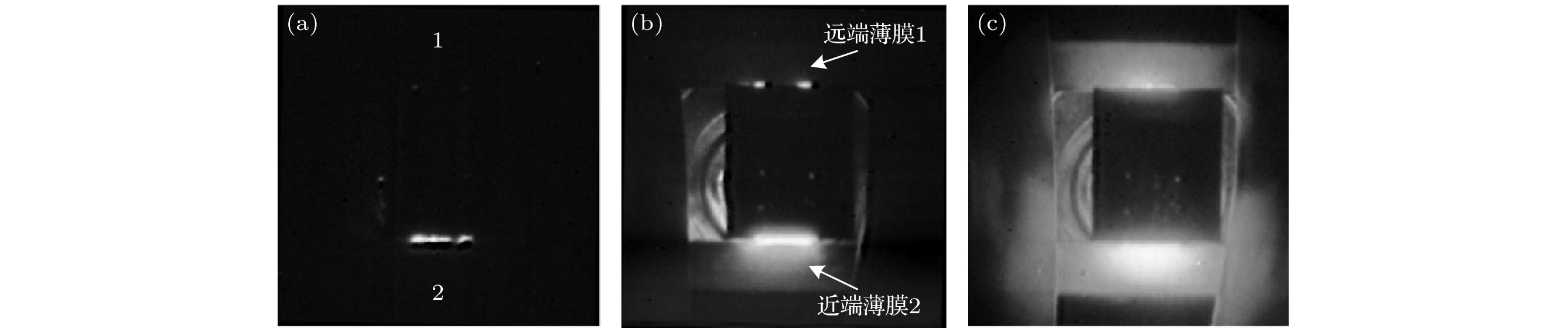
图 12 双侧非对称铝膜负载实验轴向可见光辐射图像(No. 16214) (a) 12.6 ns; (b) 33.6 ns; (c) 75.6 ns. 薄膜1对应远端位置, 薄膜2对应近端位置
Fig. 12. Optical end-on self-emission images for the asymmetric structure load with double foils (No. 16214): (a) Shot time at 12.6 ns; (b) shot time at 33.6 ns; (c) shot time at 75.6 ns. Foil 1 corresponds to the far side, and foil 2 corresponds to the near side.
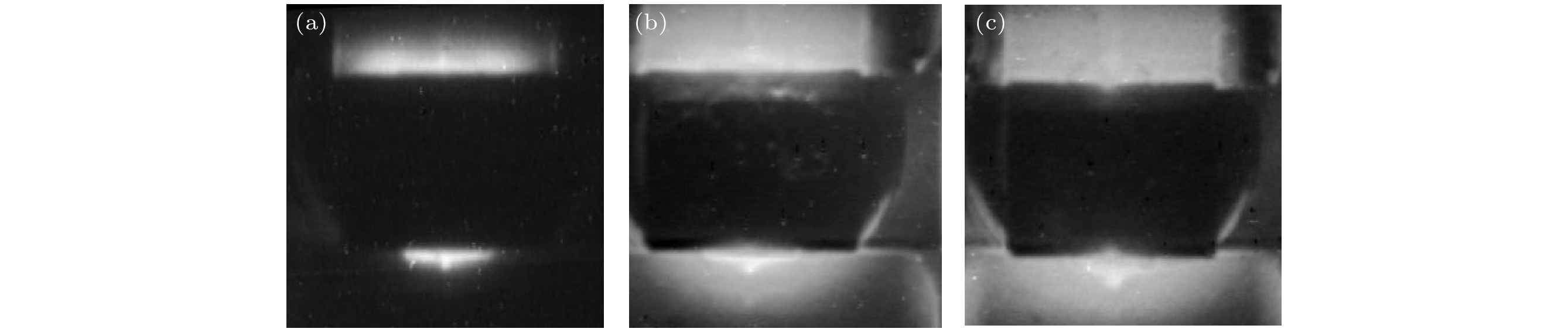
图 13 双侧对称型铝膜负载实验轴向可见光图像(No. 19110) (a) 79 ns; (b) 99 ns; (c) 119 ns
Fig. 13. Optical end-on self-emission images for the symmetric structure load with double foils (No. 19110): (a) Shot time at 79 ns; (b) shot time at 99 ns; (c) shot time at 119 ns.

图 14 20 μm铝膜电爆炸过程轴向可见光自辐射诊断图像序列. 图像经过伪色处理, 相对灰度值与伪色域对应关系如右侧标尺所示
Fig. 14. Diagnosed images sequence of axial visible end-on self-emission in exploding experiments of 20 μm Al foils. Images are treated with false-color where color scale is shown on the right.
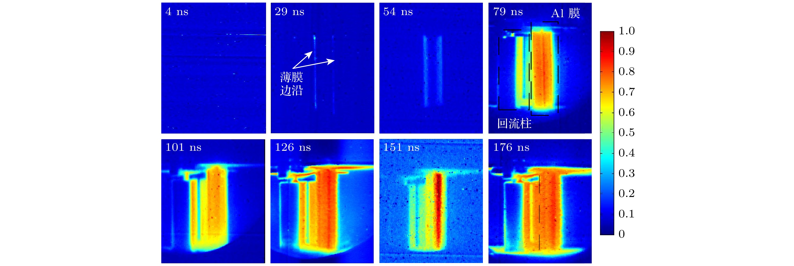
图 15 20 μm铝膜电爆炸过程截面可见光自辐射诊断图像序列. 图像经过了伪色处理, 相对灰度值与伪色域对应关系如右侧标尺所示. 相机拍摄方向与薄膜界面法向成45°
Fig. 15. Diagnosed images sequence of surface self-emission in exploding experiments of 20 μm Al foils. Images are treated with false-color where color scale is shown on the right. The shooting angle are 45° relative to foil surface orientation.
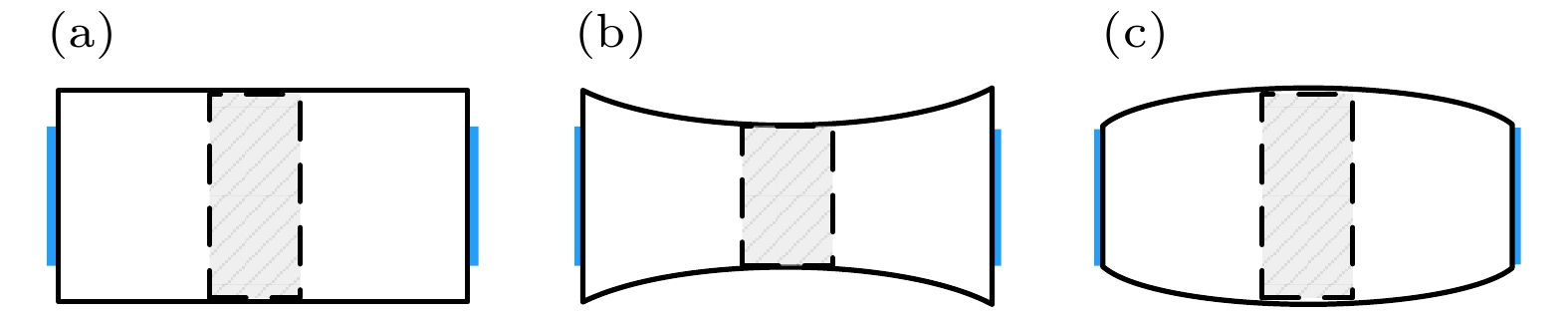
图 16 阴极片结构设计 (a) 常规结构; (b) 内凹型结构: (c) 外凸型结构. 阴影区为与回流柱连接区, 蓝色区域为薄膜连接区
Fig. 16. Different designed cathode plate structure: (a) Normal structure; (b) inner fovea structure; (c) outer fovea structure. Shadow regions connect the backpost and blue regions connect metal foils.
表 1 反场构型平面薄膜负载参数
Table 1. Parameters of the planar foils.
负载结构
类型材料M 膜厚
h/μm膜宽b/mm 膜长
l/mm回流柱厚d2/mm 边界距1
d1/mm边界距2
d3/mm双侧对称型 铝 20 10 20 10 5 5 双侧异距型 铝 20 10 20 10 15 5  下载: 导出CSV
-
[1] Ryutov D D, Derzon M S, Matzen M K 2000 Rev. Mod. Phys. 72 167
Google Scholar
[2] Haines M G 2011 Plasma Phys. Controlled Fusion 53 093001
Google Scholar
[3] Chittenden J P, Lebedev S V, Bland S N, Ruiz-Camacho J, Beg F N, Haines M G 2001 Laser Part. Beams 19 323
Google Scholar
[4] Zhigalin A S, Rousskikh A G, Oreshkin V I, Chaikovsky S A, Ratakhin N A, Kuznetsov V V 2014 International Congress On Energy Fluxes And Radiation Effects Tomsk, Russia, September 21–26, 2014 012027
[5] Oreshkin V I 2008 Phys. Plasmas 15 092103
Google Scholar
[6] 丁宁, 张扬, 刘全, 肖德龙, 束小健, 宁成 2009 物理学报 58 1083
Google Scholar
Ding N, Zhang Y, Liu Q, Xiao D L, Shu X J, Ning C 2009 Acta Phys. Sin 58 1083
Google Scholar
[7] Lebedev S V, Beg F N, Bland S N, Chittenden J P, Dangor A E, Haines M G, Pikuz S A, Shelkovenko T A 2001 Laser Part. Beams 19 355
Google Scholar
[8] Jones B, Deeney C, McKenney J L, Garasi C J, Mehlhorn T A, Robinson A C, Wunsch S E, Bland S N, Lebedev S V, Chittenden J P, Bott S C, Ampleford D J, Palmer J B, Rapley J, Hall G N, Oliver B V 2005 Phys. Rev. Lett. 95 225001
Google Scholar
[9] Chittenden J P, Jennings C A 2008 Phys. Rev. Lett. 101 055005
Google Scholar
[10] Sinars D B, Slutz S A, Herrmann M C, McBride R D, Cuneo M E, Peterson K J, Vesey R A, Nakhleh C, Blue B E, Killebrew K, Schroen D, Tomlinson K, Edens A D, Lopez M R, Smith I C, Shores J, Bigman V, Bennett G R, Atherton B W, Savage M, Stygar W A, Leifeste G T, Porter J L 2010 Phys. Rev. Lett. 105 185001
Google Scholar
[11] Lebedev S V, Beg F N, Bland S N, Chittenden J P, Dangor A E, Haines M G, Kwek K H, Pikuz S A, Shelkovenko T A 2001 Phys. Plasmas 8 3734
Google Scholar
[12] Bland S N, Lebedev S V, Chittenden J P, Ampleford D J, Tang G 2004 Phys. Plasmas 11 4911
Google Scholar
[13] 刘永棠, 盛亮, 李阳, 张金海, 孟伦, 李豪卿, 袁媛, 孙铁平, 欧阳晓平 2021 物理学报 70 065203
Google Scholar
Liu Y T, Sheng L, Li Y, Zhang J H, Meng L, Li H Q, Yuan Y, Sun T P, Ouyang X P 2021 Acta Phys. Sin. 70 065203
Google Scholar
[14] Mikitchuk D, Cvejic M, Doron R, Kroupp E, Stollberg C, Maron Y, Velikovich A L, Ouart N D, Giulianli J L, Mehlhorn T A, Yu E P, Fruchtman A 2019 Phys. Rev. Lett. 122 045001
Google Scholar
[15] Lebedev S V, Beg F N, Bland S N, Chittenden J P, Dangor A E, Haines M G, Pikuz S A, Shelkovenko T A 2000 Phys. Rev. Lett. 85 98
Google Scholar
[16] 孟伦 2018 硕士学位论文(长沙: 国防科技大学)
Meng L 2018 M. S. Thesis (Changsha: National University of Defense Technology) (in Chinese)
[17] Clayson T, Lebedev S V, Suzuki-Vidal F, Burdiak G C, Halliday J W D, Hare J D, Ma J, Suttle L G, Tubman E R 2018 IEEE Trans. Plasma Sci. 46 3734
Google Scholar
[18] Burdiak G C, Lebedev S V, Bland S N, Clayson T, Hare J, Suttle L, Suzuki-Vidal F, Garcia D C, Chittenden J P, Bott-Suzuki S, Ciardi A, Frank A, Lane T S 2017 Phys. Plasmas 24 072713
Google Scholar
[19] Lebedev S V, Frank A, Ryutov D D 2019 Rev. Mod. Phys. 91 025002
Google Scholar
[20] Bott-Suzuki S C, Caballero Bendixsen L S, Cordaro S W, Blesener I C, Hoyt C L, Cahill A D, Kusse B R, Hammer D A, Gourdain P A, Seyler C E, Greenly J B, Chittenden J P, Niasse N, Lebedev S V, Ampleford D J 2015 Phys. Plasmas 22 052710
Google Scholar
[21] 盛亮 2007 博士学位论文 (北京: 清华大学)
Sheng L 2007 Ph. D. Dissertation (Beijing: Tsinghua University) (in Chinese)
[22] Davis J, Gondarenko N A, Velikovich A L 1997 Appl. Phys. Lett. 70 170
Google Scholar
[23] Strickler T S, Gilgenbach R M, Johnston M D, Yue Ying L 2003 IEEE Trans. Plasma Sci. 31 1384
Google Scholar
[24] 王亮平, 韩娟娟, 吴坚, 郭宁, 吴刚, 李岩, 邱爱慈 2010 物理学报 59 8685
Google Scholar
Wang L P, Han J J, Wu J, Guo N, Wu G, Li Y, Qiu A C 2010 Acta Phys. Sin 59 8685
Google Scholar
[25] Esaulov A A, Velikovich A L, Kantsyrev V L, Mehlhorn T A, Cuneo M E 2006 Phys. Plasmas 13 120701
Google Scholar
[26] Esaulov A A, Kantsyrev V L, Safronova A S, Velikovich A L, Cuneo M E, Jones B, Struve K W, Mehlhorn T A 2008 Phys. Plasmas 15 052703
Google Scholar
[27] Velikovich A L, Sokolov I V, Esaulov A A 2002 Phys. Plasmas 9 1366
Google Scholar
[28] Hu Min, Kusse B R 2005 Phys. Plasmas 12 102701
Google Scholar

 下载:
下载:
计量
- 文章访问数: 6300
- PDF下载量: 57
- 被引次数: 0
