


-
超导纳米线单光子探测器(SNSPD)是综合性能最优异的新型单光子探测器之一, 而传统的单像元SNSPD不具备空间分辨力, 且光敏面小, 光学耦合效率存在瓶颈, 因此, 研制大面积阵列器件是自由空间光子探测等应用的关键. 然而, 由于器件光敏面由大量超导纳米线组成, 研发大面积的阵列SNSPD面临工艺复杂、成品率低、制备困难等问题. 本文设计了一种超大面积纳米线阵列结构, 利用电子束抗蚀剂氢倍半硅氧烷(HSQ)曝光后可形成氧化硅电学隔离层的特点, 仅使用简化二维工艺即可完成大阵列SNSPD的制备, 对多层结构的传统立体工艺实现了降维. 器件经过行方向并联测量, 未发现坏点, 成品率高, 且实现了基础的成像功能验证. 此外, 本设计中采用了全超导电极以减少电阻热效应, 并在像元内增设了串并联电阻, 从而均分偏置电流, 同时能够可选地扩展阵列规模. 本工作为超大型阵列 SNSPD 的设计与制备提供了一种思路, 并有望应用于百万像素阵列 SNSPD 的制备, 与高效读出电路结合实现兼备大视场和高灵敏度的焦平面光子探测与成像系统.
-
关键词:
- 超导纳米线单光子探测器 /
- 阵列器件 /
- 工艺优化 /
- 平面隔离层
Superconducting nanowire single-photon detector (SNSPD) is one of the most mainstream single-photon detectors at present, which possesses excellent comprehensive performance, including low time jitter, high efficiency, low dark count, and wide spectrum. However, the traditional single-pixel SNSPD suffers a lack of spatial resolution and a small photosensitive surface, which becomes a bottleneck associated with optical coupling efficiency. In addition, a single-pixel detector has no ability to resolving the photon number, whose working speed cannot be further improved due to the existence of dead time. While array devices can make up for the above deficiencies. Therefore, the development of a large-area SNSPD array is the key to free-space photon detection and other applications. In recent years, the relevant researches have been conducted and great progress has been achieved. However, the large-area SNSPD array is facing some intractable problems, including complex process, low yield, and difficult fabrication, owing to the photosensitive surface consisting of a large number of superconducting nanowires. Photons imaging is verified with this device. At present, in the existing studies mainly used is the three-dimensional technology with complicated process steps to fabricate large array SNSPDs. How to simplify the process has become a research focus. In this work, we design an ultra-large area nanowire array structure and propose an innovative plane process. Taking advantage of the property that the electron beam resists HSQ (hydrogen silsesquioxane polymer) forming a silicon oxide electrical isolation layer after exposure, we fabricate a large array SNSPD with a simplified two-dimensional process and realize dimensionality reduction for the traditional three-dimensional process of a multilayer structure. By measurement in parallel, the devices enjoy high yield with no bad points found. In addition, a full-superconducting electrode is adopted in our design to reduce the thermal effect of resistors. We add series and parallel resistors in the pixels to divide the bias current evenly and expand the array scale optionally. At the same time, we also offer the design details of array SNSPDs, the related simulation of hot spots to verify the rationality of the design, the optimization of the preparation conditions of array devices, measurement scheme formulation, and other related work. This work provides an idea for designing and fabricating ultra-large array SNSPD, which is expected to be applied to the fabrication of megapixel array SNSPDs. Combined with an efficient readout circuit, a focal plane photon detection and imaging system with both a large field of view and high sensitivity can be realized. -
Keywords:
- superconducting nanowire single photon detector /
- array device /
- process optimization /
- plane isolating layer
[1] Chang J, Los J W N, Tenorio-Pearl J O, et al. 2021 APL Photonics 6 036114
 Google Scholar
[2] Reddy D V, Nerem R R, Nam S W, Mirin R P, Verma V B 2020 Optica 7 1649
Google Scholar
[3] Korzh B, Zhao Q Y, Allmaras J P, et al. 2020 Nat. Photonics 14 250
Google Scholar
[4] Hochberg Y, Charaev I, Nam S W, Verma V, Colangelo M, Berggren K K 2019 Phys. Rev. Lett. 123 151802
Google Scholar
[5] Verma V B, Korzh B, Walter A B, et al. 2021 APL Photonics 6 056101
Google Scholar
[6] Marsili F, Bellei F, Najafi F, Dane A E, Dauler E A, Molnar R J, Berggren K K 2012 Nano Lett. 12 4799
Google Scholar
[7] Gol’tsman G N, Okunev O, Chulkova G, et al. 2001 Appl. Phys. Lett. 79 705
Google Scholar
[8] Chen L, Schwarzer D, Verma V B, et al. 2017 Accounts of Chemical Research San Francisco, CA, USA, April 2–6, 2017 pp1400–1409
[9] Allmaras J P, Beyer A D, Briggs R M, et al. 2017 Conference on Lasers and Electro-Optics San Jose, California, USA, May 14–19, 2017 pJTh3E.7
[10] Altmann Y, McLaughlin S, Padgett M J, Goyal V K, Hero A O, Faccio D 2018 Science 361 eaat2298
Google Scholar
[11] Wei K, Zhang W, Tang Y L, You L, Xu F 2019 Phys. Rev. A 100 022325
Google Scholar
[12] JP 3-14, Space Operations, CH 1, 26 October 2020, Joint Chiefs of Staff, https://www.jcs.mil/Portals/36/Documents/Doctrine/pubs/jp3_14ch1.pdf [2022-7-28]
[13] Zhao T Q, Jin S Z, Feng A M, Zhao C L, Shi Y, Xu R, Chen Y, Zhou Y D 2019 Annual Conference of Chinese-Society-of-Optical-Engineering(CSOE)-Quantum Information Technology (AOPC) Beijing, China, July 7–9, 2019 p1133907
[14] Morimoto K, Ardelean A, Wu M L, Ulku A C, Antolovic I M, Bruschini C, Charbon E 2020 Optica 7 346
Google Scholar
[15] Cusini I, Berretta D, Conca E, Incoronato A, Madonini F, Maurina A A, Nonne C, Riccardo S, Villa F 2022 Front. Phys. 10 906671
Google Scholar
[16] Morimoto K, Iwata J, Shinohara M, et al. 2021 2021 IEEE International Electron Devices Meeting (IEDM) San Francisco, CA, USA, December 11–16, 2021 pp20.2.1–20.2.4
[17] 胡小龙, 胡南, 邹锴, 孟赟, 许亮, 冯一帆 2022 激光技术 46 1
Google Scholar
Hu X L, Hu N, Zou K, Meng Y, Xu L, Feng Y F 2022 Laser Technol. 46 1
Google Scholar
[18] Miki S, Yamashita T, Wang Z, Terai H 2014 Opt. Express 22 7811
Google Scholar
[19] Zhu D, Zhao Q Y, Choi H, Lu T J, Dane A E, Englund D, Berggren K K 2018 Nat. Nanotechnol. 13 596
Google Scholar
[20] Doerner S, Kuzmin A, Wuensch S, Charaev I, Boes F, Zwick T, Siegel M 2017 Appl. Phys. Lett. 111 032603
Google Scholar
[21] Gaggero A, Martini F, Mattioli F, Chiarello F, Cernansky R, Politi A, Leoni R 2019 Optica 6 823
Google Scholar
[22] Miki S, Miyajima S, China F, Yabuno M, Terai H 2021 Opt. Lett. 46 6015
Google Scholar
[23] Verma V B, Horansky R, Marsili F, et al. 2014 Appl. Phys. Lett. 104 788
Google Scholar
[24] Wollman E E, Verma V B, Lita A E, Farr W H, Shaw M D, Mirin R P, Woo Nam S 2019 Opt. Express 27 35279
Google Scholar
[25] Allmaras J P, Wollman E E, Beyer A D, Briggs R M, Korzh B A, Bumble B, Shaw M D 2020 Nano Lett. 20 2163
Google Scholar
[26] Ma J, Song W G, Liao G X 2010 Chin. Phys. B 19 128901
Google Scholar
[27] Chen Q, Zhang B, Zhang L, et al. 2020 IEEE Photonics J. 12 1
Google Scholar
-

图 1 器件设计 (a) 行列复用结构示意图, 图中的每个矩形代表一个像元, 其中包含了超导纳米线结构. 在行方向上添加正负交替的偏置电流, 电流分配到每一行的各像元上, 然后通过列方向输出线接到地端. 列和行上的放大器被用来读取光子检测事件. 在没有光子吸收的时候, 整个阵列的行列读出线上均检测不到相应的脉冲, 而当某一个像元(如橙色像元)吸收光子后, 其超导态被破坏, 此时会在它所在的行和列上产生极性相反的两个脉冲, 通过对行与列的输出脉冲计数即可确定SNSPD响应像素的位置. 该读出方式结构相对简单, 规模易扩展, 其主要问题在于像元的不均匀性可能会带来电流的重分配问题, 且该方法并不具备光子数分辨能力. (b) 阵列SNSPD三维结构图. (c) 行列电极示意图. (d) 隔离层结构示意图, 通过对行列相交处的小范围区域进行电子束曝光, 显影后形成的氧化硅可充分覆盖暴露的行连接线, 紧接着在氧化硅上制备顶层金电极, 即可在不接触行连接线的同时, 从上方跨越式地将底层列电极相连. 采用此方法制备的隔离层覆盖面积小, 以此可以保证超导薄膜直接在衬底上生长而不需要在氧化层上生长, 从而进一步确保纳米线的质量. (e) 纳米线探测区域示意图. (f) 像元内部结构示意图, 主要包括蜿蜒纳米线、用于扩展阵列数的15个并联电阻(浅绿色)以及用于保证电流均匀分配的1个串联电阻(浅灰色). 占空比达44%
Fig. 1. Device design: (a) Schematic of the row-column multiplexing array. Each rectangle in the figure represents a pixel that contains an SNSPD. Alternating positive and negative bias currents are added in the row direction and distributed to each pixel (in each row), which are connected to the grounding terminal through the output line in the column direction. Amplifiers on rows and columns are used to read photon detection events. In the absence of photon absorption, the whole array output lines have an undetectable corresponding pulse. When a pixel (such as the orange pixel) absorbs photons, its superconducting state will be destroyed, which generates two pulses with opposite polarities in the direction of the row and column. The SNSPD response pixel can be located by counting the row-column output pulse. The structure of the readout is relatively simple, and its scale is easy to expand. The main problem lies in the inhomogeneity of pixels, which may lead to current redistribution. Furthermore, it suffers from a lack of photon number resolution capability. (b) Three-dimensional structure of the SNSPD array. (c) Diagram of the row-column electrode. (d) Diagram of the isolation layer. With electron beam exposure to a small area at the intersection of rows and columns, the silicon oxide formed after development can fully cover the exposed row connection lines. Then, the top gold electrode can be fabricated on silicon oxide, which connects the bottom column electrode from above without touching the row connection lines. In our methods, the fabricated isolation layer occupies a small coverage area, which ensures that the superconducting film grows directly on the substrate rather than on the oxide layer to further ensure the quality of the nanowire. (e) Diagram of the nanowire detection area. (f) Diagram of the internal structure of pixels, which includes sinuous nanowires, 15 parallel resistors for expanding the number of arrays, and 1 series resistor ensuring an even current distribution. Fill factor: 44%.
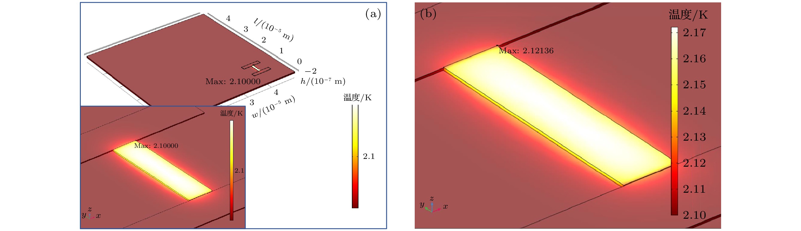
图 2 串联电阻可行性验证 (a) 典型偏置电流仿真结果; (b) 100倍偏置电流仿真结果. 仿真中采用的参考材料分别为Si衬底、100 nm电阻Au支架、40 nm Ti电阻. 仿真设置环境是2.1 K, 理论上更高工作温度下电阻焦耳热不会对纳米线功能造成影响
Fig. 2. Feasibility verification of series resistors: (a) Simulation results of typical bias current; (b) simulation results of 100 times bias current. The reference materials used in the simulation are a Si substrate, 100 nm resistor Au bracket, and 40 nm Ti resistor. The simulation was conducted at 2.1 K. Theoretically, joule heat in the resistors will not affect the function of the nanowire at higher working temperatures.
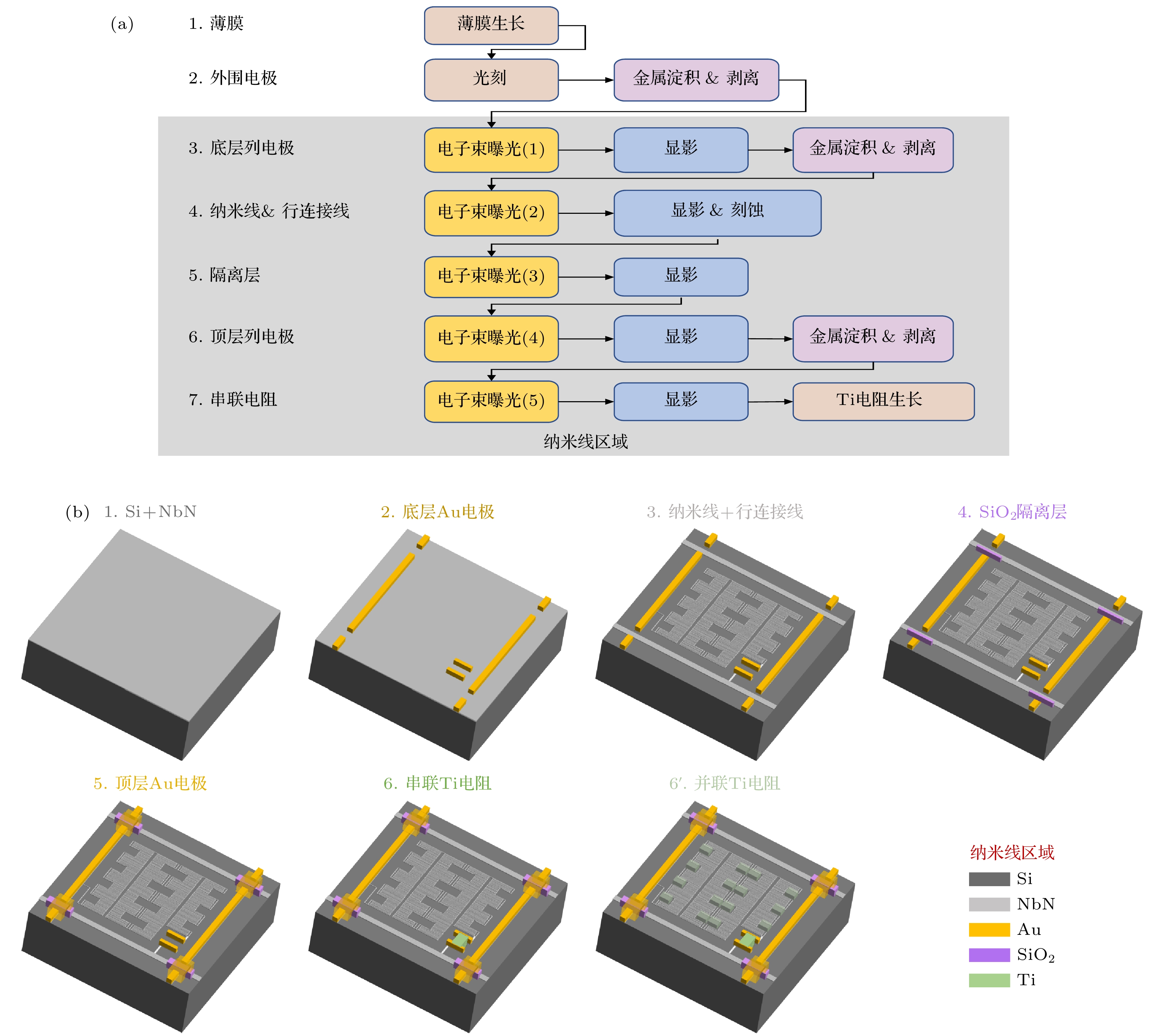
图 3 工艺流程设计 (a) 工艺流程图; (b) 纳米线区域工艺流程的三维示意图, 与图3(a)中步骤3—7可关联, 且各结构并未按比例绘制
Fig. 3. Design of fabrication process: (a) Flow chart of fabrication; (b) a three-dimensional diagram of the fabrication process of nanowire area, which is associated with steps 3 to 7 in Fig. 3(a). The structures are not drawn to scale.
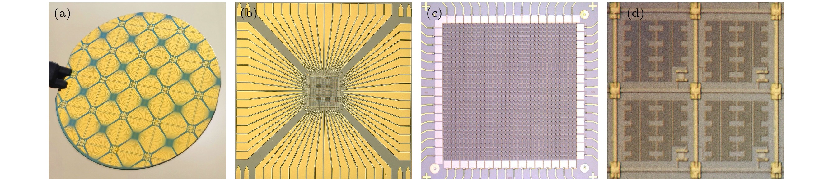
图 4 阵列器件光学图片 (a) 样品实物图; (b) 器件预览; (c) 纳米线区域光学显微镜图像; (d) 像元内部结构光学显微镜图像
Fig. 4. Optical image of device: (a) The sample chips on wafer; (b) device preview; (c) optical microscope image of nanowire area; (d) optical microscope image for internal structure of pixels.
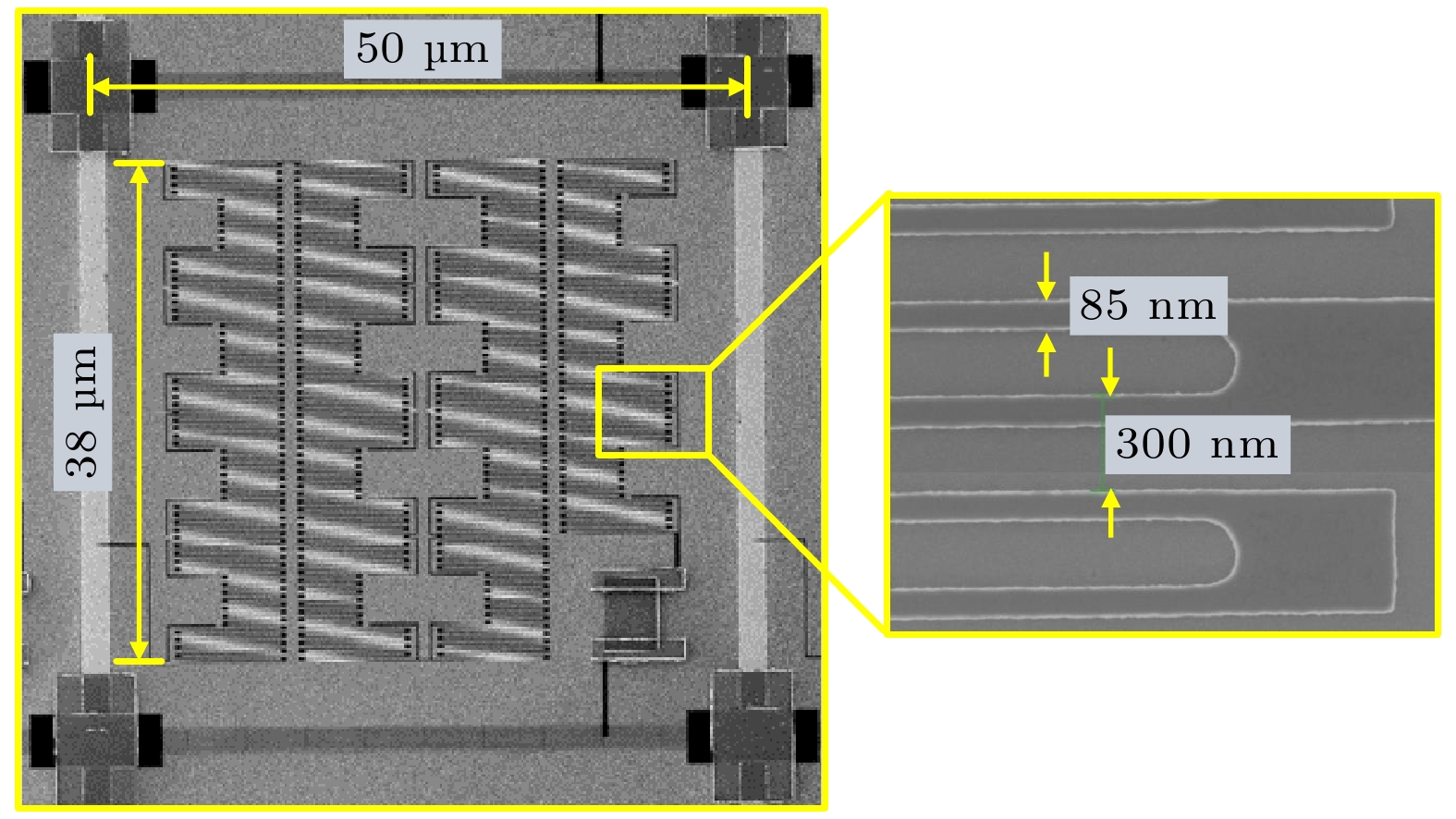
图 5 一个像元的超导纳米线扫描电子显微镜图
Fig. 5. Scanning electron microscope image of a superconducting nanowire for a pixel in the fabrication device.

图 6 纳米线区域剂量优化 (a) 单器件内标定纳米线线宽的采样点示意图; (b) 不同剂量下线宽的区域分布情况, 其中图例显示的是纳米线-图形校正区域-行连接线的剂量; (c) 各剂量下同器件线宽偏差因子, 灰线表示极差, 红线表示相对平均偏差. 以上为某次实验的6个剂量组合条件下获得的线宽数据, 已将剂量不合适的情况排除(剂量过小时纳米线易移位、断裂; 剂量过大时线条边缘粗糙、易粘连). 实验过程中每批次将同时曝光16个器件, 曝光阶段纳米线、图形校正区域及行连接线三种结构均采用一定范围的剂量分布, 在研究阶段, 此方法可保证每次实验都有数个器件的剂量合适, 能有效减小仪器不稳定性造成的影响
Fig. 6. Dose optimization in the nanowire area: (a) Diagram of sampling points for calibrating nanowires in a single device. (b) Distribution of line width at different doses. The legend represents the dose of the nanowire-graphic correction area-row connection line. (c) Line width deviation factor of the same device at each dose. The gray line indicates the range, and the red line indicates the relative mean deviation. The above are line width data obtained under the conditions of six dose combinations (in one experiment), and the case of an inappropriate dose has been excluded (the nanowire is easy to shift and break when the dose is too small, while the line edge is rough and easy to stick when the dose is too large). Sixteen devices are exposed in each batch at the same time, and an appropriate dose distribution is adopted for nanowires, graph correction areas and row connection lines. In the research stage, this method ensures that there are several devices that enjoy the appropriate dose in each experiment and effectively reduces the negative influence caused by instrument instability.
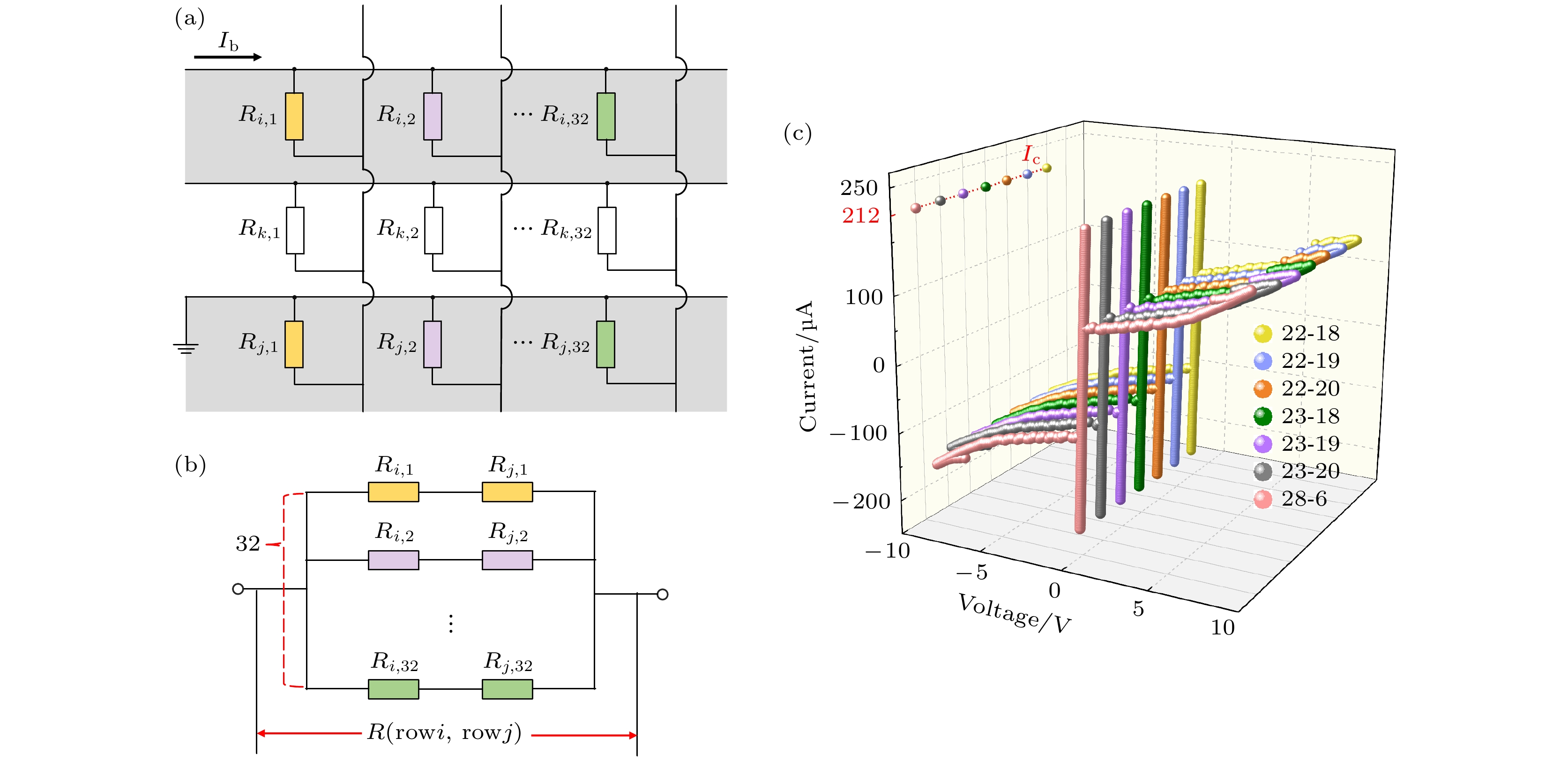
图 7 阵列器件均匀性测量, 其中i表示行号, j表示列号 (a) 简化的阵列行-行(列-列)连接示意图; (b) 简化的阵列行-行(列-列)连接等效电路图; (c) I-V特性曲线均匀性测量结果, 其中Ic为超导临界电流, T = 4.2 K
Fig. 7. Homogeneity measurement for array devices: (a) Simplified schematic of array row-row (column-column) connections; (b) simplified equivalent circuit diagram for array row-row (column-column) connections; (c) homogeneity measurement results (I-V curves), where Ic represents the superconductor critical current. T = 2.4 K.
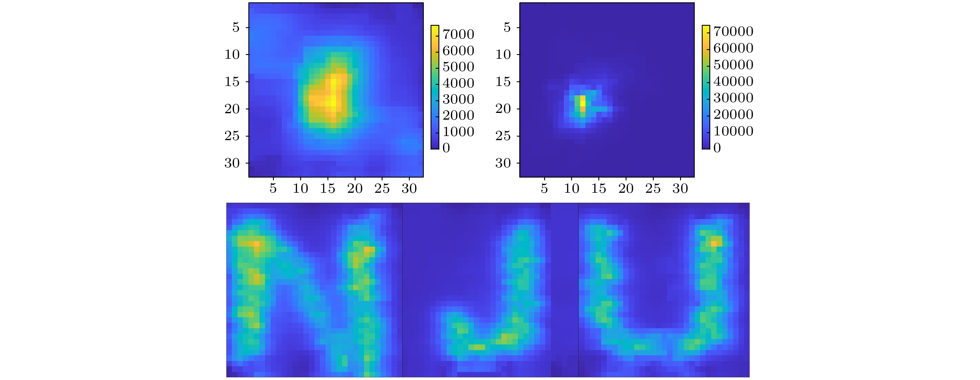
图 8 阵列器件被用于光子探测, 实现对不同大小光斑的成像, 以及书写的“NJU”图像效果(图中的纵坐标和横坐标分别表示行和列编号, 右侧颜色条表示每一帧积分时间100 ms时各像元的光子计数值)
Fig. 8. Devices are used for photon detection to achieve imaging of light spots of different sizes, as well as the written “NJU” image. The vertical and horizontal coordinates in the figure represent row and column numbers respectively, and the color bar on the right represents the photon counting value of each pixel at the integration time per frame of 100 ms. The vertical and horizontal coordinates in the figure represent row and column numbers respectively, and the color bar on the right represents the photon counting value of each pixel at the integration time per frame of 100 ms.
-
[1] Chang J, Los J W N, Tenorio-Pearl J O, et al. 2021 APL Photonics 6 036114
Google Scholar
[2] Reddy D V, Nerem R R, Nam S W, Mirin R P, Verma V B 2020 Optica 7 1649
Google Scholar
[3] Korzh B, Zhao Q Y, Allmaras J P, et al. 2020 Nat. Photonics 14 250
Google Scholar
[4] Hochberg Y, Charaev I, Nam S W, Verma V, Colangelo M, Berggren K K 2019 Phys. Rev. Lett. 123 151802
Google Scholar
[5] Verma V B, Korzh B, Walter A B, et al. 2021 APL Photonics 6 056101
Google Scholar
[6] Marsili F, Bellei F, Najafi F, Dane A E, Dauler E A, Molnar R J, Berggren K K 2012 Nano Lett. 12 4799
Google Scholar
[7] Gol’tsman G N, Okunev O, Chulkova G, et al. 2001 Appl. Phys. Lett. 79 705
Google Scholar
[8] Chen L, Schwarzer D, Verma V B, et al. 2017 Accounts of Chemical Research San Francisco, CA, USA, April 2–6, 2017 pp1400–1409
[9] Allmaras J P, Beyer A D, Briggs R M, et al. 2017 Conference on Lasers and Electro-Optics San Jose, California, USA, May 14–19, 2017 pJTh3E.7
[10] Altmann Y, McLaughlin S, Padgett M J, Goyal V K, Hero A O, Faccio D 2018 Science 361 eaat2298
Google Scholar
[11] Wei K, Zhang W, Tang Y L, You L, Xu F 2019 Phys. Rev. A 100 022325
Google Scholar
[12] JP 3-14, Space Operations, CH 1, 26 October 2020, Joint Chiefs of Staff, https://www.jcs.mil/Portals/36/Documents/Doctrine/pubs/jp3_14ch1.pdf [2022-7-28]
[13] Zhao T Q, Jin S Z, Feng A M, Zhao C L, Shi Y, Xu R, Chen Y, Zhou Y D 2019 Annual Conference of Chinese-Society-of-Optical-Engineering(CSOE)-Quantum Information Technology (AOPC) Beijing, China, July 7–9, 2019 p1133907
[14] Morimoto K, Ardelean A, Wu M L, Ulku A C, Antolovic I M, Bruschini C, Charbon E 2020 Optica 7 346
Google Scholar
[15] Cusini I, Berretta D, Conca E, Incoronato A, Madonini F, Maurina A A, Nonne C, Riccardo S, Villa F 2022 Front. Phys. 10 906671
Google Scholar
[16] Morimoto K, Iwata J, Shinohara M, et al. 2021 2021 IEEE International Electron Devices Meeting (IEDM) San Francisco, CA, USA, December 11–16, 2021 pp20.2.1–20.2.4
[17] 胡小龙, 胡南, 邹锴, 孟赟, 许亮, 冯一帆 2022 激光技术 46 1
Google Scholar
Hu X L, Hu N, Zou K, Meng Y, Xu L, Feng Y F 2022 Laser Technol. 46 1
Google Scholar
[18] Miki S, Yamashita T, Wang Z, Terai H 2014 Opt. Express 22 7811
Google Scholar
[19] Zhu D, Zhao Q Y, Choi H, Lu T J, Dane A E, Englund D, Berggren K K 2018 Nat. Nanotechnol. 13 596
Google Scholar
[20] Doerner S, Kuzmin A, Wuensch S, Charaev I, Boes F, Zwick T, Siegel M 2017 Appl. Phys. Lett. 111 032603
Google Scholar
[21] Gaggero A, Martini F, Mattioli F, Chiarello F, Cernansky R, Politi A, Leoni R 2019 Optica 6 823
Google Scholar
[22] Miki S, Miyajima S, China F, Yabuno M, Terai H 2021 Opt. Lett. 46 6015
Google Scholar
[23] Verma V B, Horansky R, Marsili F, et al. 2014 Appl. Phys. Lett. 104 788
Google Scholar
[24] Wollman E E, Verma V B, Lita A E, Farr W H, Shaw M D, Mirin R P, Woo Nam S 2019 Opt. Express 27 35279
Google Scholar
[25] Allmaras J P, Wollman E E, Beyer A D, Briggs R M, Korzh B A, Bumble B, Shaw M D 2020 Nano Lett. 20 2163
Google Scholar
[26] Ma J, Song W G, Liao G X 2010 Chin. Phys. B 19 128901
Google Scholar
[27] Chen Q, Zhang B, Zhang L, et al. 2020 IEEE Photonics J. 12 1
Google Scholar

 下载:
下载:
计量
- 文章访问数: 11469
- PDF下载量: 224
- 被引次数: 0
