


-
无载流子注入型发光二极管(简称无注入型LED)因其简单的器件结构有望应用于Micro-LED、纳米像元发光显示等新型微显示技术. 由于没有外部载流子注入, 无注入型LED的内部载流子输运行为无法直接用传统的PN结理论进行描述. 因此, 建立无注入型LED的载流子输运模型对于理解其工作机理和提高器件性能具有重要意义. 本文根据无注入型LED的器件结构, 结合PN结理论建立无注入型LED的载流子输运数学模型. 基于该数学模型解释器件的工作原理, 获得器件的载流子输运特性, 揭示感应电荷区长度、内部PN结压降与外加驱动电压频率的关系. 根据建立的数学模型提出了针对无注入型LED器件设计的建议: 1)减小感应电荷区掺杂浓度, 可有效提高内部LED的压降; 2)利用PN结的隧穿效应, 可有效提高器件内部LED的压降; 3)使用正负方波驱动可以获得比正弦驱动更大的内部LED压降. 本文有关无注入型LED的载流子输运模型的研究有望为改善无注入型LED器件结构、优化工作模式提供理论指导.Non-carrier-injection light-emitting diodes (NCI-LEDs) are expected to be widely used in the next-generation micro-display technologies, including Micro-LEDs and nano-pixel light-emitting displays due to their simple device structures. However, because there is no external charge carrier injection, the internal carrier transport behavior of the NCI-LED cannot be described by using the traditional PN junction and LED theory. Therefore, establishing a carrier-transport model for the NCI-LED is of great significance in understanding its working mechanism and improving device performance. In this work, carrier transport mathematical model of the NCI-LED is established and the mechanical behavior of charge-carrier transport is analyzed quantitatively. Based on the mathematical model, the working mechanism of the NCI-LED is explained, the carrier transport characteristics of the device are obtained. Additionally, the key features, including the length of the induced charge region, the forward biased voltage across the internal PN junction, and the reverse biased voltage across the internal PN junction are studied. Their relationships with the applied frequency of the applied driving voltage are revealed. It is found that both the forward bias and reverse bias of the internal PN junction increase with the driving frequency. When the driving frequency reaches a certain value, the forward bias and the reverse bias of the PN junction will be maintained at a maximum value. Moreover, the length of the induced charge region decreases with the increase of the driving frequency, and when the frequency reaches a certain value, the induced charge region will always be in the state of exhaustion. According to the mathematical model, suggestions for the device optimization design are provided below. 1) Reducing the doping concentration of the induced charge region can effectively increase the voltage drop across the internal LED; 2) employing the tunneling effect occurring in the reverse-biased PN junction can effectively improve the electroluminescence intensity; 3) using the square-wave driving voltage can obtain a larger voltage drop across the internal LED and increase the electroluminescence intensity. This work on the carrier transport model is expected to e present a clear physical figure for understanding the working mechanism of NCI-LED, and to provide a theoretical guidance for optimizing the device structure.
-
Keywords:
- light-emitting diode /
- non-carrier injection /
- carrier transport model /
- numerical calculation
[1] 邰建鹏, 郭伟玲, 李梦梅, 邓杰, 陈佳昕 2020 物理学报 69 177301
 Google Scholar
Tai J P, Guo W L, Li M M, Deng J, Chen J X 2020 Acta Phys. Sin. 69 177301
Google Scholar
[2] Zhou X, Tian P, Sher C W, Wu J, Liu H, Liu R, Kuo H C 2020 Prog. Quantum Electron. 71 100263
[3] Lee H E, Shin J H, Park J H, Hong S K, Park S H, Lee S H, Lee J H, Kang I S, Lee K J 2019 Adv. Funct. Mater. 29 1808075
Google Scholar
[4] Bower C A, Meitl M A, Raymond B, Radauscher E, Cok R, Bonafede S, Gomez D, Moore T, Prevatte C, Fisher B, Rotzoll R, Melnik G A, Fecioru A, Trindade A J 2017 Photonics Res. 5 A23
Google Scholar
[5] Wu C, Wang K, Zhang Y, Zhou X, Guo T 2021 J. Phys. Chem. Lett 12 3522
Google Scholar
[6] Li S, Waag A 2012 J. Appl. Phys. 111 071101
Google Scholar
[7] Jung B O, Bae S Y, Lee S, Kim S Y, Lee J Y, Honda Y, Amano H 2016 Nanoscale Res. Lett. 11 215
Google Scholar
[8] 高承浩, 徐峰, 张丽, 赵德胜, 魏星, 车玲娟, 庄永漳, 张宝顺, 张晶 2020 物理学报 69 027802
Google Scholar
Gao C H, Xu F, Zhang L, Zhao D S, Wei X, Che L J, Zhuang Y Z, Zhang B S, Zhang J 2020 Acta Phys. Sin. 69 027802
Google Scholar
[9] Ogawa K, Hachiya R, Mizutani T, Ishijima S, Kikuchi A 2016 Phys. Status Solidi A 214 1600613
Google Scholar
[10] Ra Y H, Wang R, Woo S Y, Djavid M, Sadaf S M, Lee J, Botton G A, Mi Z 2016 Nano Lett. 16 4608
Google Scholar
[11] Choi H, Jeon C, Dawson M 2004 IEEE Electr. Device L. 25 277
Google Scholar
[12] Gong Z, Zhang H, Gu E, Griffin C, Dawson M D, Poher V, Kennedy G, French P, Neil M 2007 IEEE T. Electron Dev. 54 2650
Google Scholar
[13] Konoplev S S, Bulashevich K A, Karpov S Y 2018 Phys. Status. Solidi. A 215 1700508
Google Scholar
[14] Adivarahan V, Wu S, Sun W, Mandavilli V, Shatalov M, Simin G, Yang J, Maruska H, Khan M A 2004 Appl. Phys. Lett. 85 1838
Google Scholar
[15] Wang K, Liu Y, Chen R, Wu C X, Zhou X T, Zhang Y A, Liu Z Q, Guo T L 2021 IEEE Electr. Device Lett. 42 1033
Google Scholar
[16] Wang K, Chen P, Chen J, Liu Y, Wu C X, Sun J, Zhou X T, Zhang Y A, Guo T L 2021 Opt. Laser Technol. 140 107044
Google Scholar
[17] Wang K, Liu Y, Wu C X, Li D, Lv S, Zhang Y, Zhou X, Guo T L 2020 Sci. Rep. 10 1
Google Scholar
[18] Wu C X, Wang K, Guo T L 2022 Nanomaterials 12 2532
Google Scholar
[19] Li W, Wang K, Li J, Wu C X, Zhang Y, Zhou X, Guo T L 2022 Nanomaterials 12 912
Google Scholar
[20] Sze S M, Li Y, Ng K K 2021 Physics of Semiconductor Devices (John Wiley & Sons)
[21] Huang F, Wang Z, Chu C, Liu Q, Li Y, Xin Z, Zhang Y, Sun Q, Zhang Z H 2022 IEEE T. Electron Dev. 69 5522
Google Scholar
-
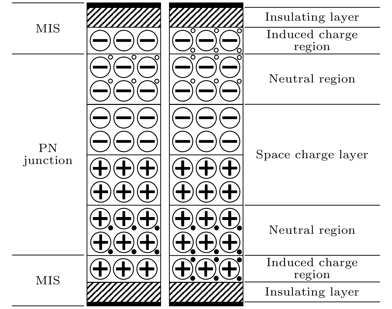
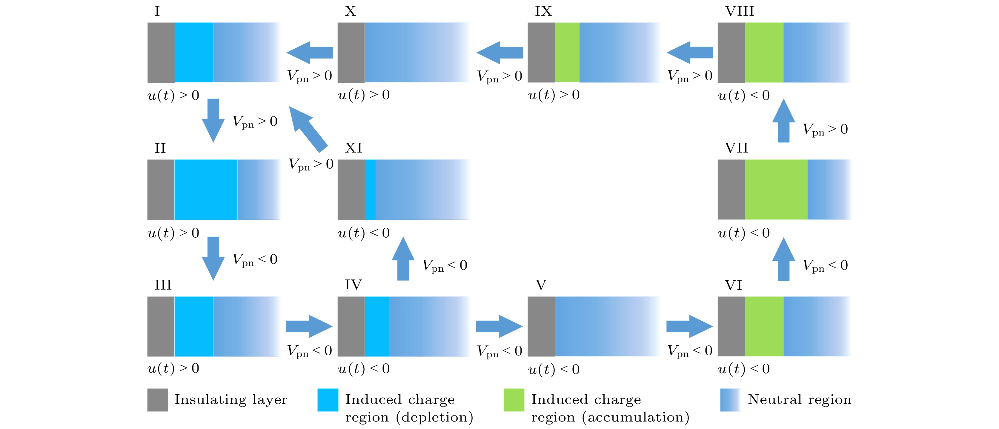
图 2 无注入型LED内部的电荷分布示意图
Fig. 2. Schematic diagram of charge distribution in non-carrier-injection LED.

图 3 外加电压、PN结电压、P区感应电荷区理想/实际长度在 (a)电压频率为40 Hz, (b)电压频率为100 Hz的变化情况; (c) 单周期内PN结电压变化; (d) 单周期内P区感应电荷区实际长度变化; (e) 不同频率下的PN结电压最大值与最小值; (f) 不同频率下的P区感应电荷区实际长度变化
Fig. 3. Applied voltage, PN junction voltage, ideal/actual length of induced charge region in P region at the voltage frequency is 40 Hz (a) and 100 Hz (b); (c) PN junction voltage in one voltage period; (d) actual length of induced charge region in the P region in one voltage period; (e) maximum/minimum PN junction voltage under different frequencies; (e) actual length of induced charge region in P region under different frequencies.
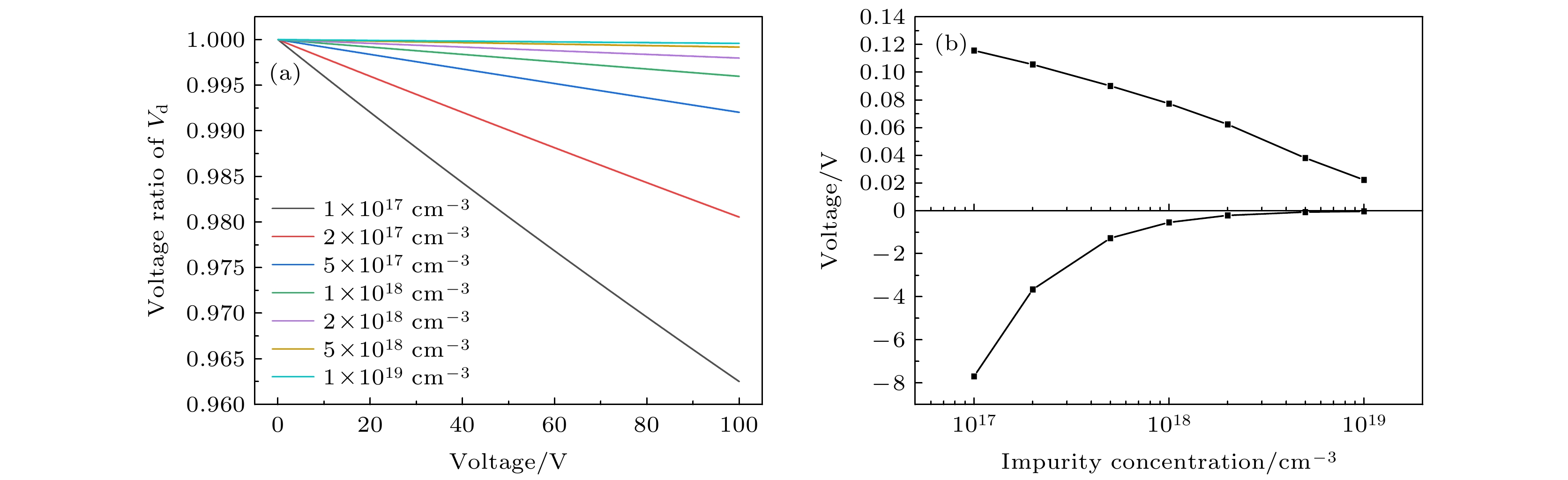
图 5 (a) 绝缘层压降占比; (b) PN结电压最大值/最小值
Fig. 5. (a) Voltage ratio of insulation layer voltage; (b) maximum/minimum PN junction voltage.

图 6 (a)单周期内PN结电压变化; (b) 单周期内P区感应电荷区实际长度变化;
Fig. 6. (a) Voltage change of PN junction in one voltage period; (b) actual length change of the induced charge region in P region in one voltage period.
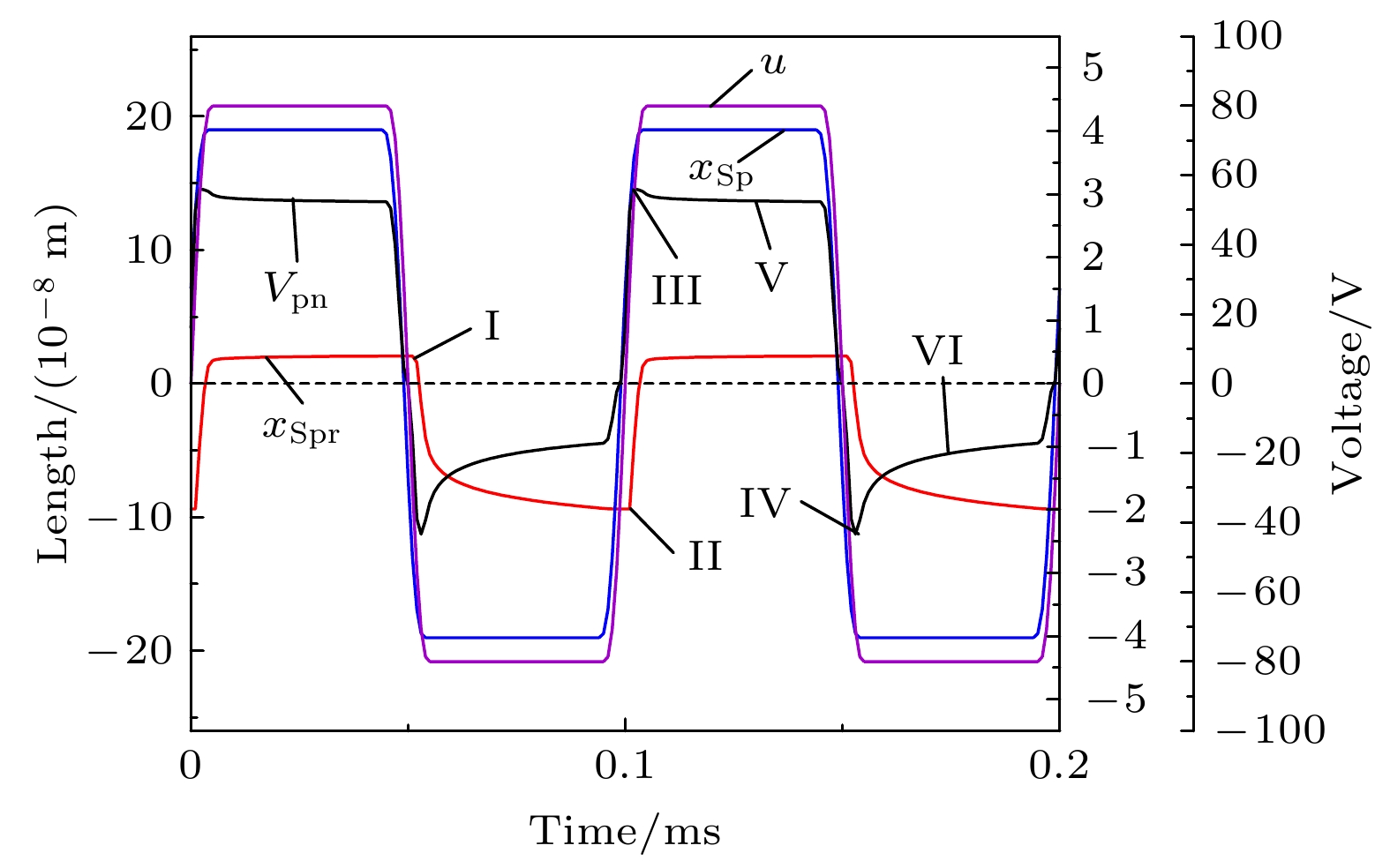
图 8 外加电压、PN结电压、P区感应电荷区理想/实际长度变化情况
Fig. 8. Applied voltage, PN junction voltage, ideal/actual length of induced charge region in P region.
-
[1] 邰建鹏, 郭伟玲, 李梦梅, 邓杰, 陈佳昕 2020 物理学报 69 177301
Google Scholar
Tai J P, Guo W L, Li M M, Deng J, Chen J X 2020 Acta Phys. Sin. 69 177301
Google Scholar
[2] Zhou X, Tian P, Sher C W, Wu J, Liu H, Liu R, Kuo H C 2020 Prog. Quantum Electron. 71 100263
[3] Lee H E, Shin J H, Park J H, Hong S K, Park S H, Lee S H, Lee J H, Kang I S, Lee K J 2019 Adv. Funct. Mater. 29 1808075
Google Scholar
[4] Bower C A, Meitl M A, Raymond B, Radauscher E, Cok R, Bonafede S, Gomez D, Moore T, Prevatte C, Fisher B, Rotzoll R, Melnik G A, Fecioru A, Trindade A J 2017 Photonics Res. 5 A23
Google Scholar
[5] Wu C, Wang K, Zhang Y, Zhou X, Guo T 2021 J. Phys. Chem. Lett 12 3522
Google Scholar
[6] Li S, Waag A 2012 J. Appl. Phys. 111 071101
Google Scholar
[7] Jung B O, Bae S Y, Lee S, Kim S Y, Lee J Y, Honda Y, Amano H 2016 Nanoscale Res. Lett. 11 215
Google Scholar
[8] 高承浩, 徐峰, 张丽, 赵德胜, 魏星, 车玲娟, 庄永漳, 张宝顺, 张晶 2020 物理学报 69 027802
Google Scholar
Gao C H, Xu F, Zhang L, Zhao D S, Wei X, Che L J, Zhuang Y Z, Zhang B S, Zhang J 2020 Acta Phys. Sin. 69 027802
Google Scholar
[9] Ogawa K, Hachiya R, Mizutani T, Ishijima S, Kikuchi A 2016 Phys. Status Solidi A 214 1600613
Google Scholar
[10] Ra Y H, Wang R, Woo S Y, Djavid M, Sadaf S M, Lee J, Botton G A, Mi Z 2016 Nano Lett. 16 4608
Google Scholar
[11] Choi H, Jeon C, Dawson M 2004 IEEE Electr. Device L. 25 277
Google Scholar
[12] Gong Z, Zhang H, Gu E, Griffin C, Dawson M D, Poher V, Kennedy G, French P, Neil M 2007 IEEE T. Electron Dev. 54 2650
Google Scholar
[13] Konoplev S S, Bulashevich K A, Karpov S Y 2018 Phys. Status. Solidi. A 215 1700508
Google Scholar
[14] Adivarahan V, Wu S, Sun W, Mandavilli V, Shatalov M, Simin G, Yang J, Maruska H, Khan M A 2004 Appl. Phys. Lett. 85 1838
Google Scholar
[15] Wang K, Liu Y, Chen R, Wu C X, Zhou X T, Zhang Y A, Liu Z Q, Guo T L 2021 IEEE Electr. Device Lett. 42 1033
Google Scholar
[16] Wang K, Chen P, Chen J, Liu Y, Wu C X, Sun J, Zhou X T, Zhang Y A, Guo T L 2021 Opt. Laser Technol. 140 107044
Google Scholar
[17] Wang K, Liu Y, Wu C X, Li D, Lv S, Zhang Y, Zhou X, Guo T L 2020 Sci. Rep. 10 1
Google Scholar
[18] Wu C X, Wang K, Guo T L 2022 Nanomaterials 12 2532
Google Scholar
[19] Li W, Wang K, Li J, Wu C X, Zhang Y, Zhou X, Guo T L 2022 Nanomaterials 12 912
Google Scholar
[20] Sze S M, Li Y, Ng K K 2021 Physics of Semiconductor Devices (John Wiley & Sons)
[21] Huang F, Wang Z, Chu C, Liu Q, Li Y, Xin Z, Zhang Y, Sun Q, Zhang Z H 2022 IEEE T. Electron Dev. 69 5522
Google Scholar


 下载:
下载:


计量
- 文章访问数: 6279
- PDF下载量: 91
- 被引次数: 0
