


-
分子与衬底之间的相互作用在有机薄膜的生长过程中起着非常重要的作用. 对于金属衬底和半金属衬底来说, 由于不同的电子结构, 二者与分子薄膜之间的相互作用会有明显的差异. 本文利用扫描隧道显微镜对比研究了二氰基蒽(DCA)分子在金属衬底Cd(0001)和半金属衬底Bi(111)上的薄膜生长. 实验发现, 在Cd(0001)衬底上, 低温沉积的DCA薄膜表现出三维生长模式, 而室温沉积的DCA薄膜表现出二维生长模式. 特别是DCA分子单层具有斜方对称的4×
$ \sqrt {13} $ 公度结构, 表明DCA与Cd(0001)之间存在较强的相互作用. 与此形成鲜明对比的是, 在半金属Bi(111)衬底上, 低温沉积的DCA薄膜表现出二维生长模式, 在分子单层中有莫尔条纹出现, 表明DCA单层是一种非公度结构, DCA与Bi(111)之间的相互作用较弱. 通过上述的对比研究可以看出, 衬底材料的电子结构和沉积温度均可影响DCA分子薄膜的结构和生长模式.The interactions between molecules and substrates play an important role in growing organic thin films. The metallic and semimetallic substrates, owing to the different electronic structures, can have distinct interactions with molecular films. Here we make a comparative study on the two-dimensional (2D) self-assemblies of dicyanoanthracene (DCA) molecules on the metallic Cd(0001) and semimetallic Bi(111) surfaces. It is found that the DCA thin film grown on Cd(0001) surface at low temperature exhibits a three-dimensional (3D) growth mode, with the monolayer islands, two-layer islands, and three-layer islands coexisting on the Cd(0001) surface. When deposited at room temperature, the DCA molecules exhibit a 2D growth mode, where the monolayer DCA adopts the 4×$\sqrt {13} $ reconstruction with respective Cd(0001). The commensurate epitaxy indicates that there is strong interaction between DCA molecules and Cd(0001). In clear contrast, the DCA molecules deposited on the semimetallic Bi(111) surface at low temperature exhibit a 2D growth mode. Furthermore, a moiré pattern with the periodicity of 2.6 nm is observed in the DCA monolayer, indicating the incommensurate epitaxy of DCA monolayer on Bi(111). This can be explained by the weak interaction between DCA and Bi(111) substrate. These results demonstrate that both of the electronic structure of substrates and substrate temperatures can be used to adjust the structures of morphology of DCA films.-
Keywords:
- dicyanoanthracene /
- sannning tunneling microscope /
- incommensurate structures /
- semimetallic substrate
[1] Forrest S R 1997 Chem. Rev. 97 1793
 Google Scholar
[2] Meyer zu Heringdorf F J, Reuter M, Tromp R 2001 Nature 412 517
Google Scholar
[3] Stingelin-Stutzmann N, Smits E, Wondergem H, Tanase C, Blom P, Smith P, De Leeuw D 2005 Nat. Mater. 4 601
Google Scholar
[4] Witte G, Wöll C H 2008 Phys. Status. Solidi. A 205 497
Google Scholar
[5] Zhang J L, Ye X, Gu C D, Han C, Sun S, Wang L, Chen W 2020 Surf. Sci. Rep. 75 100481
Google Scholar
[6] Pawin G, Wong K L, Kim D, Sun D, Bartels L, Hong S, Rahman T S, Carp R, Marsella M 2008 Angew. Chem. Int. Ed. 47 8442
Google Scholar
[7] Liljeroth P, Swart I, Paavilainen S, Repp J, Meyer G 2010 Nano Lett. 10 2475
Google Scholar
[8] Zhang J, Shchyrba A, Nowakowska S, Meyer E, Jung T A, Muntwiler M 2014 Chem. Commun. 50 12289
Google Scholar
[9] Zhang L Z, Wang Z F, Huang B, Cui B, Wang Z, Du S X, Gao H J, Liu F 2016 Nano Lett. 16 2072
Google Scholar
[10] Fuchs M, Liu P T, Schwemmer T, Sangiovanni G, Thomale R, Franchini C, Sante D D 2020 J. Phys. Mater. 3 025001
Google Scholar
[11] Kumar D, Krull C, Yin Y F, Medhekar N V, Schiffrin A 2019 ACS Nano 13 11882
Google Scholar
[12] Kumar D, Hellerstedt J, Field B, Lowe B, Yin Y F, Medhekar N V, Schiffrin A 2021 Adv. Funct. Mater. 31 2106474
Google Scholar
[13] Yan L H, Pohjavirta I, Alldritt B, Liljeroth P 2019 ChemPhysChem 20 2297
Google Scholar
[14] López L H, Zulaica I P, Downing C A, Piantek M, Fujii J, Serrate D, Ortega J E, Bartolomé F, Checa J L 2021 Nanoscale 13 5216
Google Scholar
[15] Kumar A, Banerjee K, Foster A S, Liljeroth P 2018 Nano Lett. 18 5596
Google Scholar
[16] Yan L H, Silveira O J, Alldritt B, Krejčí O, Foster A S, Liljeroth P 2021 Adv. Funct. Mater. 31 2100519
Google Scholar
[17] Yan L H, Silveira O J, Alldritt B, Kezilebieke S, Foster A S, Liljeroth P 2021 ACS Nano 15 17813
Google Scholar
[18] Chauhan H S, Ilver L, Nilsson P O, Kanski J, Karlsson K 1993 Phys. Rev. B 48 4729
Google Scholar
[19] Stark R W, Falicov L M 1967 Phys. Rev. Lett. 19 795
Google Scholar
[20] Daniuk S, Jarlborg T, Kontrym-Sznajd G, Majsnerowski J, Stachowiak H 1989 J. Phys. Condens. Matter. 1 8397
Google Scholar
[21] Rienstra-Kiracofe J C, Tschumper G S, Schaefer H F, Nandi S, Ellison G B 2002 Chem. Rev. 102 231
Google Scholar
[22] Tao M L, Xiao H F, Sun K, Tu Y B, Yuan H K, Xiong Z H, Wang J Z, Xue Q K 2017 Phy. Rev. B. 96 125410
Google Scholar
[23] Pascual J I, Bihlmayer G, Koroteev Y M, H P, Ceballos G, Hansmann M, Horn K, Chulkov E V, Blügel S, Echenique P M, Hofmann P 2004 Phys. Rev. Lett. 93 196802
Google Scholar
[24] Nagao T, Sadowski J T, Saito M, Yaginuma S, Fujikawa Y, Kogure T, Ohno T, Hasegawa Y, Hasegawa S, Sakurai T 2004 Phys. Rev. Lett. 93 105501
Google Scholar
[25] Koroteev Y M, Bihlmayer G, Chulkov E V, Blügel S 2008 Phys. Rev. B 77 045428
Google Scholar
[26] Hooks D E, Fritz T, Ward M D 2001 Adv. Mater. 13 227
Google Scholar
[27] Thayer G E, Sadowski J T, Zu Heringdorf F M, Sakurai T, Tromp R M 2005 Phys. Rev. Lett. 95 256106
Google Scholar
-
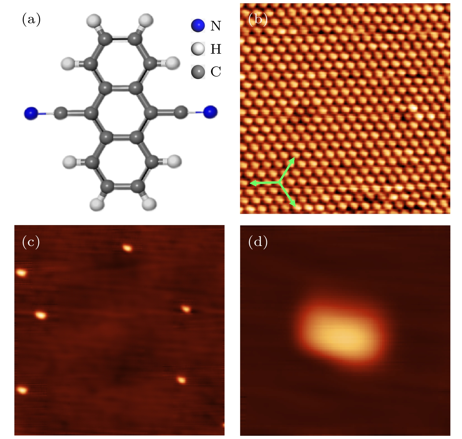
图 1 吸附在Cd(0001)表面的DCA分子 (a) DCA分子的结构模型; (b) Cd(0001)衬底的原子分辨图, 扫描区域为6 nm× 6 nm, 扫描偏压为1.0 V; (c) 吸附在Cd(0001)衬底上的孤立DCA分子, 78 nm× 78 nm, 3.0 V; (d) 单个DCA分子的放大图, 9 nm× 9 nm, 1.9 V
Fig. 1. Individual DCA molecules adsorbed on Cd(0001): (a) Molecular modeling of DCA; (b) STM image of the Cd(0001) surface with hexagonal lattice, the scanning area is 6 nm× 6 nm, the scanning bias is 1.0 V; (c) isolated DCA molecules adsorbed on Cd(0001) at 77 K, 78 nm × 78 nm, 3.0 V; (d) close-up view of a single DCA molecule, 9 nm× 9 nm, 1.9 V.
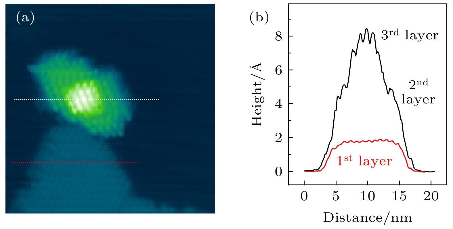
图 2 低温沉积形成的DCA三维岛 (a) DCA单层岛、二层岛和三层岛同时出现在Cd(0001)表面上, 扫描区域为50 nm× 50 nm, 扫描偏压为2.8 V; (b) 沿图(a)中的白色和红色虚线所做的高度剖面图; 第1层, 第2层和第3层岛的高度分别是1.8 Å, 2.9 Å和3.7 Å
Fig. 2. Formation of 3D islands of DCA by low-temperature deposition: (a) A three-layer DCA island coexists with a monolayer-island on the same substrate terrace, the scanning area is 50 nm× 50 nm, the scanning bias is 2.8 V; (b) height profile lines across the white and red dotted lines in panel (a). The heights of first layer, second layer, and third layer are 1.8 Å, 2.9 Å, and 3.7 Å, respectively.

图 3 第二层DCA岛的不稳定性 (a)—(c) 连续STM扫描导致第二层DCA岛的形状和尺寸发生的变化, 扫描偏压依次为 (a) 3.0 V, (b) 2.5 V, (c) 2.5 V, 扫描区域均为10 nm × 10 nm
Fig. 3. Instability of the second layer DCA island: (a)–(c) Three sequential STM images of a second layer of DCA island, showing the variation of island size and shape. The bias voltage varies from 3.0 V (a), 2.5 V (b), to 2.5 V (c), the scanning area is all 10 nm × 10 nm.
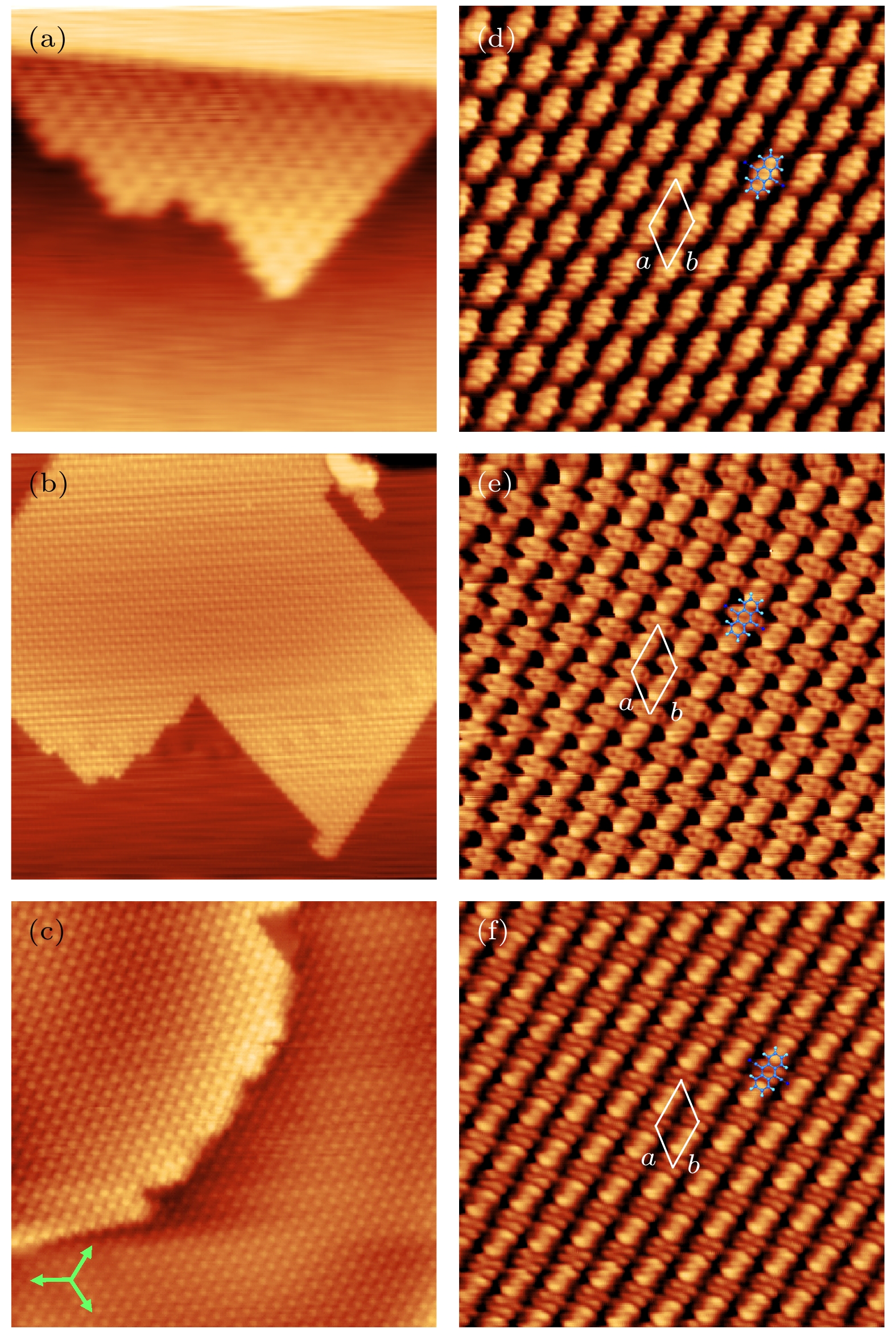
图 4 室温沉积时形成的DCA自组装单层 (a) 出现在Cd(0001)台阶处的DCA单层岛(θ = 0.4 ML); (b) 出现在Cd(0001)台面上的DCA单层岛(θ = 0.7 ML); (c) DCA分子单层(θ = 1 ML)表现出4 ×
$ \sqrt {13} $ 重构; (d)—(f) DCA分子单层的偏压依赖图(10 nm× 10 nm). 各图的扫描区域和偏压分别为: (a)为20 nm× 20 nm, 0.18 V; (b) 50 nm× 50 nm, 2.8 V; (c) 30 nm× 30 nm, 0.8 V; (d) –0.4 V; (e) 0.3 V; (f) 0.5 VFig. 4. DCA self-assembled monolayer formed at room temperature: (a) A small monolayered island of DCA appeared at step edge of substrate, θ = 0.4 ML; (b) a large monolayer island of DCA appeared on the substrate terrace, θ = 0.7 ML; (c) the full monolayer DCA on Cd(0001) showing 4 ×
$ \sqrt {13} $ reconstruction; (d)–(f) bias-dependent STM images of DCA monolayer (10 nm × 10 nm). All the scanning area and bias are (a) 20 nm× 20 nm, 0.18 V; (b) 50 nm× 50 nm, 2.8 V; (c) 30 nm× 30 nm, 0.8 V; (d) –0.4 V; (e) 0.3 V; (f) 0.5 V.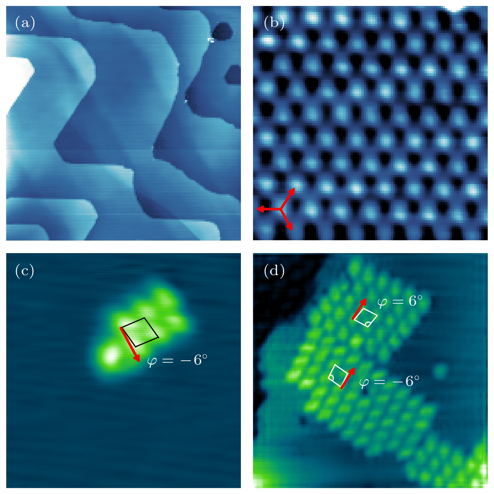
图 5 Bi(111)衬底上的DCA分子团簇和单层岛 (a) Bi(111)薄膜的STM形貌图, 扫描区域为230 nm× 230 nm, 扫描偏压为2.5 V; (b) Bi(111)薄膜的原子分辨图, 4 nm× 4 nm, 0.4 V; (c) 在Bi(111)表面上形成的DCA七分子团簇, 10 nm × 10 nm, 0.4 V; (d) 两个互为镜像的DCA单层岛, 16 nm× 16 nm, 0.4 V
Fig. 5. DCA molecular clusters and monolayer islands on Bi(111): (a) Morphology of Bi(111) thin films, the scanning area is 230 nm × 230 nm, the scanning bias is 2.5 V; (b) atomic-resolution STM image of the Bi(111) surface showing the hexagonal lattice, 4 nm × 4 nm, 0.4 V; (c) a seven-molecule cluster of DCA formed on Bi(111), 10 nm × 10 nm, 0.4 V; (d) two mirror domains of DCA monolayer with opposite misorientation angles respective to the Bi(111) lattice, 16 nm × 16 nm, 0.4 V.
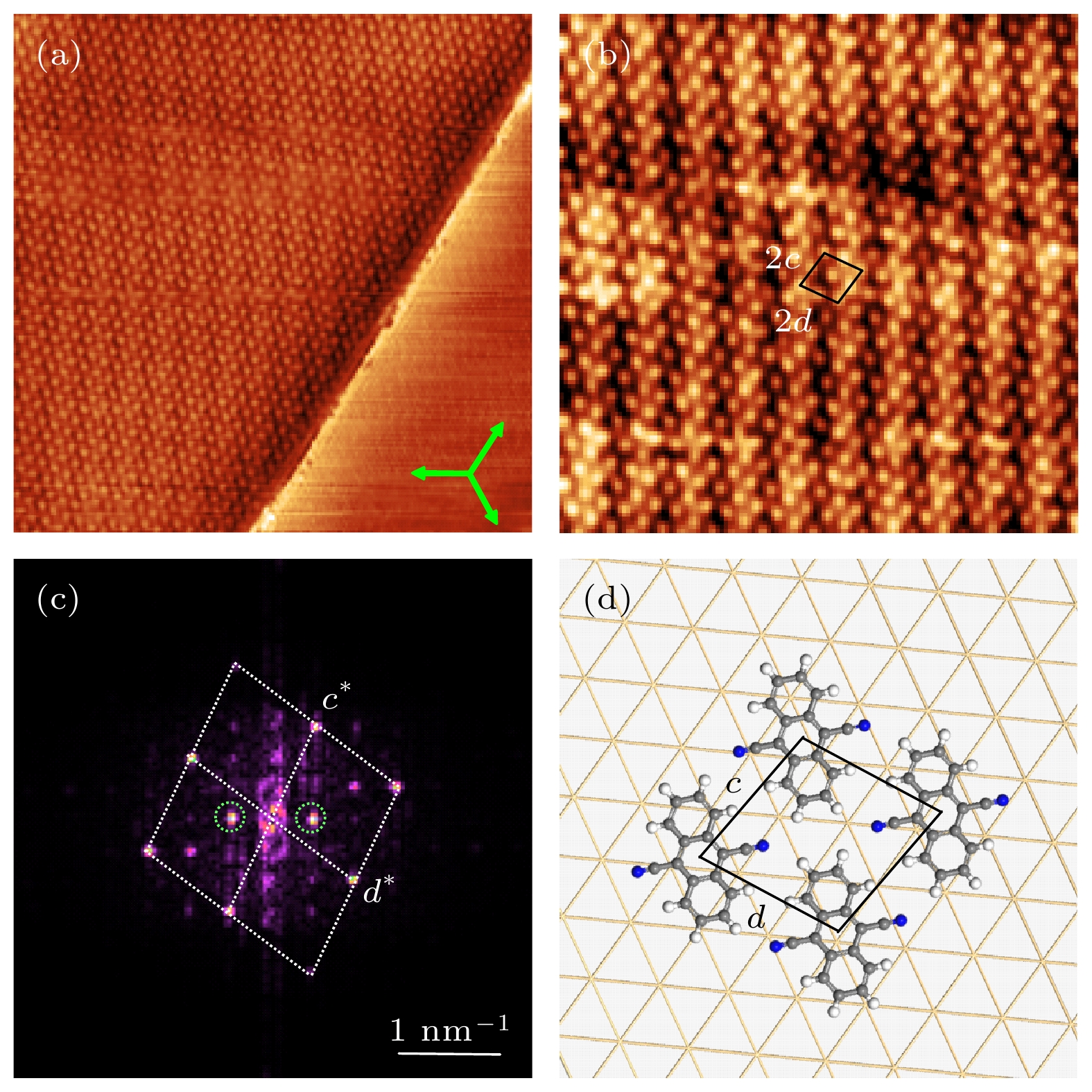
图 6 Bi(111)表面上非公度的DCA分子单层 (a) DCA单层中出现的莫尔条纹, 0.8 ML, 扫描区域为40 nm × 40 nm, 扫描偏压为0.48 V; (b) 莫尔条纹的高分辨图, 26 nm × 26 nm, 0.48 V; (c) 图(b)的快速傅里叶变换(FFT)图, 其中c*和d*分别是晶格c和d的的倒格子矢量, 绿色圆圈中的斑点是莫尔条纹的倒格子矢量; (d) DCA分子单层的结构示意图
Fig. 6. Incommensurate DCA monolayer on Bi(111): (a) Moiré pattern appeared in the DCA monolayer, 0.8 ML, the scanning area is 40 nm × 40 nm, the scanning bias is 0.48 V; (b) close-up view of the moiré pattern, 26 nm × 26 nm, 0.48 V; (c) fast Fourier transformation (FFT) of (b), where c* and d* are the reciprocal lattice vectors of DCA monolayer, the circled spots are the reciprocal lattice vectors of moiré pattern; (d) schematic model of the DCA monolayer.
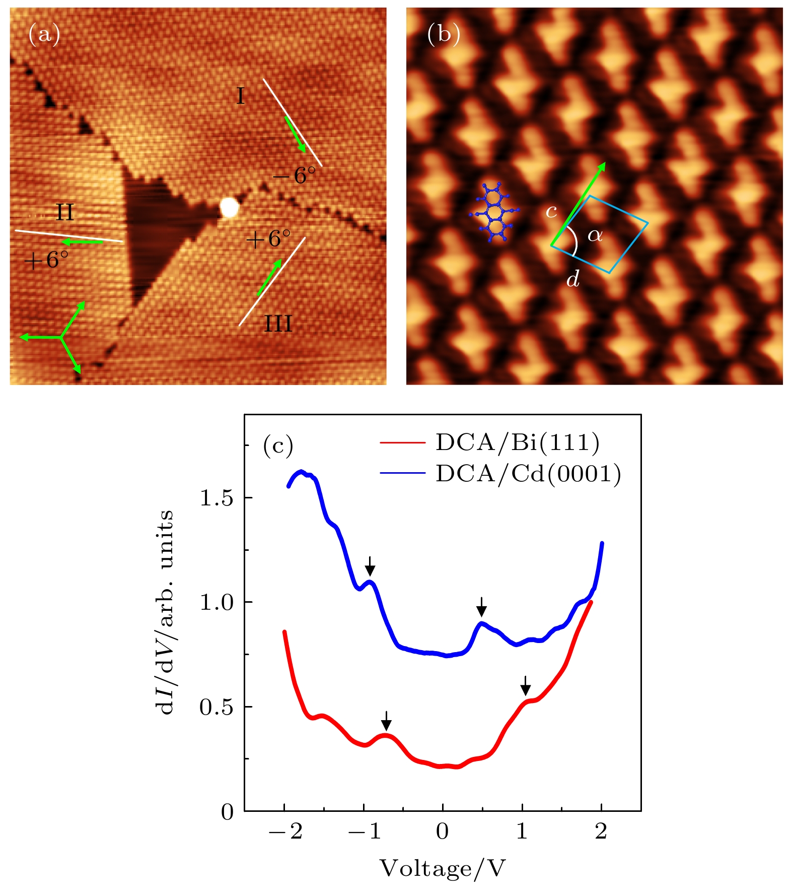
图 7 DCA分子单层中的转动畴 (a) 3个不同方向的DCA转动畴, 扫描区域为50 nm× 50 nm, 扫描偏压为0.56 V; (b) 畴区III中的DCA分子的高分辨图, 6 nm× 6 nm, 0.12 V; (c) 在DCA/Cd(0001)和DCA/Bi(111)分子层中采集的扫描隧道谱, 针尖高度控制在U = 1.0 V, I = 20 pA的条件下
Fig. 7. Rotational domains in the DCA monolayer: (a) Three rotational domains of DCA monolayer with different directions, the scanning area is 50 nm× 50 nm, the scanning bias is 0.56 V; (b) high-resolution STM image of the DCA molecules in domain III, 6 nm× 6 nm, 0.12 V; (c) scanning tunneling spectra acquired on top of DCA molecules on Cd(0001) and Bi(111), respectively. The tip was kept at the condition of U = 1.0 V, I = 20 pA.
-
[1] Forrest S R 1997 Chem. Rev. 97 1793
Google Scholar
[2] Meyer zu Heringdorf F J, Reuter M, Tromp R 2001 Nature 412 517
Google Scholar
[3] Stingelin-Stutzmann N, Smits E, Wondergem H, Tanase C, Blom P, Smith P, De Leeuw D 2005 Nat. Mater. 4 601
Google Scholar
[4] Witte G, Wöll C H 2008 Phys. Status. Solidi. A 205 497
Google Scholar
[5] Zhang J L, Ye X, Gu C D, Han C, Sun S, Wang L, Chen W 2020 Surf. Sci. Rep. 75 100481
Google Scholar
[6] Pawin G, Wong K L, Kim D, Sun D, Bartels L, Hong S, Rahman T S, Carp R, Marsella M 2008 Angew. Chem. Int. Ed. 47 8442
Google Scholar
[7] Liljeroth P, Swart I, Paavilainen S, Repp J, Meyer G 2010 Nano Lett. 10 2475
Google Scholar
[8] Zhang J, Shchyrba A, Nowakowska S, Meyer E, Jung T A, Muntwiler M 2014 Chem. Commun. 50 12289
Google Scholar
[9] Zhang L Z, Wang Z F, Huang B, Cui B, Wang Z, Du S X, Gao H J, Liu F 2016 Nano Lett. 16 2072
Google Scholar
[10] Fuchs M, Liu P T, Schwemmer T, Sangiovanni G, Thomale R, Franchini C, Sante D D 2020 J. Phys. Mater. 3 025001
Google Scholar
[11] Kumar D, Krull C, Yin Y F, Medhekar N V, Schiffrin A 2019 ACS Nano 13 11882
Google Scholar
[12] Kumar D, Hellerstedt J, Field B, Lowe B, Yin Y F, Medhekar N V, Schiffrin A 2021 Adv. Funct. Mater. 31 2106474
Google Scholar
[13] Yan L H, Pohjavirta I, Alldritt B, Liljeroth P 2019 ChemPhysChem 20 2297
Google Scholar
[14] López L H, Zulaica I P, Downing C A, Piantek M, Fujii J, Serrate D, Ortega J E, Bartolomé F, Checa J L 2021 Nanoscale 13 5216
Google Scholar
[15] Kumar A, Banerjee K, Foster A S, Liljeroth P 2018 Nano Lett. 18 5596
Google Scholar
[16] Yan L H, Silveira O J, Alldritt B, Krejčí O, Foster A S, Liljeroth P 2021 Adv. Funct. Mater. 31 2100519
Google Scholar
[17] Yan L H, Silveira O J, Alldritt B, Kezilebieke S, Foster A S, Liljeroth P 2021 ACS Nano 15 17813
Google Scholar
[18] Chauhan H S, Ilver L, Nilsson P O, Kanski J, Karlsson K 1993 Phys. Rev. B 48 4729
Google Scholar
[19] Stark R W, Falicov L M 1967 Phys. Rev. Lett. 19 795
Google Scholar
[20] Daniuk S, Jarlborg T, Kontrym-Sznajd G, Majsnerowski J, Stachowiak H 1989 J. Phys. Condens. Matter. 1 8397
Google Scholar
[21] Rienstra-Kiracofe J C, Tschumper G S, Schaefer H F, Nandi S, Ellison G B 2002 Chem. Rev. 102 231
Google Scholar
[22] Tao M L, Xiao H F, Sun K, Tu Y B, Yuan H K, Xiong Z H, Wang J Z, Xue Q K 2017 Phy. Rev. B. 96 125410
Google Scholar
[23] Pascual J I, Bihlmayer G, Koroteev Y M, H P, Ceballos G, Hansmann M, Horn K, Chulkov E V, Blügel S, Echenique P M, Hofmann P 2004 Phys. Rev. Lett. 93 196802
Google Scholar
[24] Nagao T, Sadowski J T, Saito M, Yaginuma S, Fujikawa Y, Kogure T, Ohno T, Hasegawa Y, Hasegawa S, Sakurai T 2004 Phys. Rev. Lett. 93 105501
Google Scholar
[25] Koroteev Y M, Bihlmayer G, Chulkov E V, Blügel S 2008 Phys. Rev. B 77 045428
Google Scholar
[26] Hooks D E, Fritz T, Ward M D 2001 Adv. Mater. 13 227
Google Scholar
[27] Thayer G E, Sadowski J T, Zu Heringdorf F M, Sakurai T, Tromp R M 2005 Phys. Rev. Lett. 95 256106
Google Scholar


 下载:
下载:


计量
- 文章访问数: 6843
- PDF下载量: 217
- 被引次数: 0
